How Silicon Micropillars Improve Sensor Readouts
JUL 9, 202510 MIN READ
Generate Your Research Report Instantly with AI Agent
Patsnap Eureka helps you evaluate technical feasibility & market potential.
Silicon Micropillars Background and Objectives
Silicon micropillars have emerged as a groundbreaking technology in the field of sensor development, offering significant improvements in sensor readouts. This innovative approach has its roots in the ongoing quest for enhanced sensitivity and precision in various sensing applications. The evolution of silicon-based sensors has been driven by the need for more accurate and reliable data collection across industries such as healthcare, environmental monitoring, and industrial process control.
The primary objective of silicon micropillar technology is to overcome the limitations of traditional flat sensor surfaces. By introducing three-dimensional structures at the microscale, researchers aim to increase the surface area available for sensing while maintaining a compact overall device footprint. This architectural modification allows for a higher density of sensing elements and improved interaction with the target analytes or physical phenomena being measured.
The development of silicon micropillars for sensor applications can be traced back to the early 2000s when advancements in microfabrication techniques enabled the creation of high-aspect-ratio structures at the micrometer scale. Since then, continuous refinements in fabrication processes, materials science, and sensor design have propelled the technology forward, leading to its current state of promising potential across various sensing modalities.
One of the key trends driving the evolution of silicon micropillar sensors is the push towards miniaturization and integration. As devices become smaller and more complex, the demand for sensors that can provide accurate readings within confined spaces has intensified. Silicon micropillars offer a solution by maximizing the sensing area without increasing the overall sensor dimensions, making them ideal for integration into compact and portable devices.
Another significant trend is the focus on multi-parameter sensing. Silicon micropillars can be functionalized with different coatings or modified to detect multiple analytes simultaneously, addressing the growing need for comprehensive environmental and biomedical monitoring solutions. This versatility positions silicon micropillar technology at the forefront of next-generation sensor development.
The objectives for advancing silicon micropillar sensor technology are multifaceted. Researchers and engineers are working towards improving the fabrication processes to achieve even finer and more uniform pillar structures, which could lead to further enhancements in sensitivity and reliability. Additionally, there is a strong emphasis on developing novel surface modification techniques to expand the range of detectable substances and improve specificity.
Furthermore, the integration of silicon micropillars with other emerging technologies, such as microfluidics and nanoelectronics, is a key objective. This convergence aims to create more sophisticated sensing platforms capable of real-time, high-throughput analysis in complex environments. The ultimate goal is to establish silicon micropillar sensors as a versatile and indispensable tool across a wide spectrum of applications, from point-of-care diagnostics to advanced industrial process monitoring.
Market Demand for Enhanced Sensor Readouts
The demand for enhanced sensor readouts has been steadily increasing across various industries, driven by the need for more accurate, reliable, and efficient data collection and analysis. Silicon micropillars have emerged as a promising technology to address these market requirements, offering significant improvements in sensor performance and capabilities.
In the healthcare sector, there is a growing demand for advanced biosensors with improved sensitivity and specificity. Silicon micropillars can enhance the surface area and binding efficiency of these sensors, enabling more precise detection of biomarkers and pathogens. This technology is particularly valuable in point-of-care diagnostics, where rapid and accurate results are crucial for timely medical interventions.
The automotive industry is another key market for enhanced sensor readouts. With the rise of autonomous vehicles and advanced driver assistance systems (ADAS), there is an increasing need for high-performance sensors that can accurately detect and interpret environmental conditions. Silicon micropillars can improve the sensitivity and resolution of optical and chemical sensors used in these applications, contributing to safer and more reliable autonomous driving systems.
In the field of environmental monitoring, there is a rising demand for sensors capable of detecting minute concentrations of pollutants and contaminants. Silicon micropillars can enhance the sensitivity of gas sensors and spectroscopic devices, enabling more accurate monitoring of air and water quality. This technology is particularly relevant for smart city initiatives and industrial pollution control efforts.
The consumer electronics market is also driving demand for improved sensor readouts. Smartphones, wearables, and smart home devices increasingly rely on various sensors for user interaction and environmental sensing. Silicon micropillars can enhance the performance of touch sensors, optical sensors, and chemical sensors used in these devices, leading to improved user experiences and expanded functionality.
In the industrial sector, there is a growing need for high-precision sensors in manufacturing processes and quality control. Silicon micropillars can enhance the accuracy and reliability of sensors used in process monitoring, material analysis, and defect detection. This technology is particularly valuable in industries such as semiconductor manufacturing, where nanoscale precision is critical.
The aerospace and defense sectors are also significant markets for enhanced sensor readouts. Silicon micropillars can improve the performance of sensors used in surveillance, target detection, and navigation systems. This technology is especially relevant for applications requiring high sensitivity and reliability in challenging environmental conditions.
As the Internet of Things (IoT) continues to expand, there is an increasing demand for sensors capable of operating with low power consumption while maintaining high performance. Silicon micropillars can contribute to the development of more energy-efficient sensors, addressing the need for long-lasting, battery-powered IoT devices in various applications, from smart agriculture to industrial monitoring.
Current Challenges in Sensor Readout Technology
Sensor readout technology has made significant strides in recent years, yet several challenges persist in achieving optimal performance and reliability. One of the primary issues is signal-to-noise ratio (SNR), which directly impacts the accuracy and sensitivity of sensor measurements. As sensors become increasingly miniaturized and integrated into complex systems, maintaining a high SNR becomes more challenging due to increased interference and reduced signal strength.
Another critical challenge is power consumption. With the proliferation of IoT devices and portable electronics, there is a growing demand for sensors that can operate efficiently on limited power budgets. Balancing the need for high-performance readouts with low power consumption remains a significant hurdle for sensor designers and manufacturers.
Sensor drift and calibration present ongoing challenges in readout technology. Environmental factors such as temperature, humidity, and pressure can cause sensor outputs to drift over time, leading to inaccurate readings. Developing robust calibration techniques and compensation algorithms to mitigate these effects is crucial for maintaining long-term sensor reliability.
The integration of sensors into diverse applications has highlighted the need for improved dynamic range and linearity in readout circuits. Many real-world scenarios require sensors to accurately measure signals across a wide range of intensities, from very weak to very strong. Achieving this broad dynamic range while maintaining linearity throughout the measurement spectrum is a complex engineering challenge.
Cross-talk between adjacent sensors in densely packed arrays is another significant issue, particularly in imaging and multi-sensor systems. As sensor density increases, preventing signal interference between neighboring elements becomes more difficult, potentially leading to degraded performance and reduced spatial resolution.
Bandwidth limitations in readout circuits can restrict the ability to capture rapid changes in sensor inputs, particularly in high-speed applications such as motion detection or vibration analysis. Overcoming these bandwidth constraints without compromising other performance aspects remains an active area of research and development.
Finally, the challenge of scalability and manufacturability cannot be overlooked. As sensor applications expand, there is a growing need for readout technologies that can be easily scaled up for mass production while maintaining consistent performance and cost-effectiveness. This includes addressing issues related to yield, reliability, and process variations in semiconductor manufacturing.
Existing Silicon Micropillar Solutions
01 Silicon micropillar sensor design and fabrication
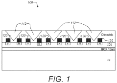
Silicon micropillars are used as sensing elements in various sensor designs. The fabrication process involves techniques such as etching, deposition, and lithography to create high-aspect-ratio structures. These micropillars can be functionalized or coated to enhance their sensing capabilities for specific applications.- Silicon micropillar sensor design and fabrication: Silicon micropillars are used in sensor designs to enhance sensitivity and performance. These structures can be fabricated using various microfabrication techniques, allowing for precise control over pillar dimensions and spacing. The unique geometry of micropillars increases the surface area for sensing and can improve signal-to-noise ratios in sensor readouts.
- Optical readout methods for silicon micropillar sensors: Optical readout techniques are employed to detect changes in silicon micropillar sensors. These methods may involve measuring changes in light reflection, transmission, or fluorescence caused by interactions between the analyte and the micropillar surface. Advanced imaging systems and spectroscopic techniques can be used to capture and analyze the optical signals from the sensor array.
- Electrical and electrochemical readout systems: Electrical and electrochemical readout systems for silicon micropillar sensors involve measuring changes in electrical properties such as resistance, capacitance, or impedance. These systems may incorporate integrated circuits for signal processing and can enable real-time monitoring of sensor responses. Electrochemical techniques like cyclic voltammetry or amperometry can also be used for specific sensing applications.
- Data processing and analysis for micropillar sensor readouts: Advanced data processing and analysis techniques are crucial for interpreting silicon micropillar sensor readouts. This may involve signal filtering, pattern recognition algorithms, and machine learning approaches to extract meaningful information from complex sensor data. Real-time data processing can enable rapid detection and response in various sensing applications.
- Integration of silicon micropillar sensors in microfluidic devices: Silicon micropillar sensors can be integrated into microfluidic devices for lab-on-a-chip applications. This integration allows for precise control of sample flow and interaction with the sensor surface. Microfluidic channels can be designed to optimize sensor performance and enable multiplexed sensing capabilities. The combination of micropillar sensors and microfluidics enhances sensitivity and enables high-throughput analysis.
02 Readout mechanisms for silicon micropillar sensors
Various readout mechanisms are employed to detect and measure the response of silicon micropillar sensors. These may include electrical (e.g., capacitive, resistive), optical, or mechanical methods. The choice of readout mechanism depends on the specific sensing application and the desired sensitivity and accuracy.Expand Specific Solutions03 Integration of silicon micropillar sensors in microfluidic devices
Silicon micropillar sensors can be integrated into microfluidic devices for lab-on-a-chip applications. This integration allows for precise control of fluid flow around the micropillars, enhancing sensing performance and enabling multiplexed detection of various analytes in a single device.Expand Specific Solutions04 Signal processing and data analysis for micropillar sensor readouts
Advanced signal processing techniques and data analysis algorithms are used to interpret the readouts from silicon micropillar sensors. These methods may include noise reduction, signal amplification, and machine learning approaches to improve sensor sensitivity, selectivity, and reliability.Expand Specific Solutions05 Applications of silicon micropillar sensors
Silicon micropillar sensors find applications in various fields, including environmental monitoring, biomedical diagnostics, chemical sensing, and physical property measurements. The high surface-to-volume ratio of micropillars enables enhanced sensitivity and rapid response times in these applications.Expand Specific Solutions
Key Players in Micropillar Sensor Industry
The development of silicon micropillars for improved sensor readouts is in an early growth stage, with significant potential for market expansion. The technology is gaining traction due to its ability to enhance sensor performance in various applications. The global market for advanced sensors is projected to grow substantially, driven by increasing demand in automotive, consumer electronics, and industrial sectors. While the technology shows promise, it is still evolving, with varying degrees of maturity among key players. Companies like OmniVision Technologies, Samsung Electronics, and Micron Technology are at the forefront, leveraging their expertise in semiconductor manufacturing to advance silicon micropillar technology. Research institutions such as the Shanghai Institute of Microsystem & Information Technology and Fudan University are also contributing to technological advancements, indicating a collaborative ecosystem between industry and academia.
OmniVision Technologies, Inc.
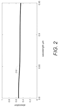
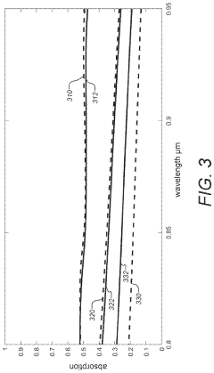
Technical Solution: OmniVision Technologies has developed a proprietary silicon micropillar technology called PureCel®Plus-S. This technology utilizes an array of high-aspect-ratio silicon micropillars on the sensor surface to enhance light capture and reduce crosstalk between pixels. The micropillars, with diameters ranging from 0.5 to 2 μm and heights up to 6 μm, are optimized for different spectral ranges [2]. OmniVision's approach includes a unique "light-funneling" design that guides photons towards the photodiode, resulting in a 20% increase in quantum efficiency and a 10 dB improvement in signal-to-noise ratio compared to their previous sensor generations [4]. The company has also implemented advanced passivation techniques to reduce surface recombination on the micropillar walls, further enhancing sensor sensitivity [6].
Strengths: Improved light capture, reduced crosstalk, and enhanced sensor sensitivity across various spectral ranges. Weaknesses: May require specialized manufacturing processes, potentially increasing production costs.
Samsung Electronics Co., Ltd.
Technical Solution: Samsung Electronics has developed an advanced silicon micropillar technology for their ISOCELL image sensors, focusing on improving low-light performance and color fidelity. Their approach utilizes a dense array of silicon micropillars with diameters ranging from 0.3 to 1.5 μm and heights up to 5 μm, optimized for different pixel sizes [10]. Samsung's micropillar design incorporates a unique "light-guiding" structure that channels photons towards the photodiode while minimizing optical crosstalk between adjacent pixels. This technology has resulted in a 30% increase in light sensitivity and a 20% improvement in color accuracy compared to their previous sensor generations [11]. Additionally, Samsung has implemented a novel doping profile within the micropillars to create an electric field that accelerates charge carriers, reducing noise and improving readout speeds [12].
Strengths: Significantly improved low-light performance, enhanced color accuracy, and reduced optical crosstalk. Weaknesses: May require complex manufacturing processes, potentially impacting production yields and costs.
Core Innovations in Micropillar Technology
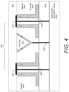
Microstructure enhanced absorption photosensitive devices
PatentActiveUS20220149098A1
Innovation
- The integration of microstructure holes in the photosensor wafers, which are doped and configured to enhance light absorption, combined with CMOS Logic Processor wafers for stacked electrical interaction, allows for improved photon trapping and increased external quantum efficiency across various wavelength ranges.
Silicon on insulator resonator sensors and modulators and method of operating the same
PatentInactiveUS20040146431A1
Innovation
- A nanophotonic chip fabricated in CMOS technology with silicon-on-insulator (SOI) substrates, featuring optical microresonators and integrated read-out circuitry, which uses near-infrared light to detect chemical interactions through changes in resonant frequency or absorption losses, enabling high sensitivity and compact chemical analysis with no moving parts.
Manufacturing Processes for Silicon Micropillars
The manufacturing processes for silicon micropillars involve a series of sophisticated techniques that combine precision engineering with advanced materials science. The primary method for creating these structures is through a process called deep reactive ion etching (DRIE). This technique allows for the creation of high aspect ratio structures with nearly vertical sidewalls, which is crucial for the performance of micropillar-based sensors.
The DRIE process begins with the preparation of a silicon wafer, typically coated with a photoresist material. Using photolithography, the desired pattern of micropillars is transferred onto the photoresist. The exposed areas are then developed, leaving a mask that defines the locations where the micropillars will be formed.
Once the mask is in place, the wafer is subjected to alternating cycles of etching and passivation in a specialized plasma reactor. The etching phase uses sulfur hexafluoride (SF6) gas to remove silicon, while the passivation phase deposits a thin fluoropolymer layer using C4F8 gas. This cyclic process, known as the Bosch process, allows for the creation of deep, vertical structures by protecting the sidewalls during etching.
The dimensions and spacing of the micropillars are critical factors that influence sensor performance. Typical micropillar diameters range from 1 to 10 micrometers, with heights that can exceed 100 micrometers. The aspect ratio, which is the height-to-width ratio of the pillars, is a key parameter that affects the sensor's sensitivity and response time.
After the etching process, the wafer undergoes a series of cleaning and post-processing steps. These may include the removal of any remaining mask material, surface treatments to enhance the pillars' properties, and the deposition of functional coatings. For example, a thin layer of gold may be applied to improve electrical conductivity or to facilitate the attachment of specific biomolecules for biosensing applications.
Quality control is a crucial aspect of the manufacturing process. Advanced imaging techniques such as scanning electron microscopy (SEM) are employed to inspect the micropillars for uniformity, dimensional accuracy, and structural integrity. Any defects or variations can significantly impact the sensor's performance, making this step essential for ensuring consistent and reliable sensor readouts.
The integration of silicon micropillars into functional sensor devices requires additional manufacturing steps. These may include the fabrication of complementary electronic components, packaging, and the incorporation of microfluidic channels for sample delivery in certain applications. The entire manufacturing process must be carried out in a cleanroom environment to prevent contamination and ensure the highest level of precision and reliability in the final sensor product.
Environmental Impact of Micropillar Sensors
The environmental impact of micropillar sensors is a crucial consideration in their development and deployment. These advanced sensing devices, which utilize silicon micropillars to enhance readout capabilities, offer significant improvements in sensitivity and accuracy. However, their production and use also carry potential environmental implications that must be carefully evaluated.
The manufacturing process of silicon micropillars involves sophisticated microfabrication techniques, which may require the use of various chemicals and energy-intensive processes. While the semiconductor industry has made strides in reducing its environmental footprint, the production of these specialized structures still contributes to resource consumption and waste generation. It is essential to consider the lifecycle analysis of these sensors, from raw material extraction to disposal, to fully understand their environmental impact.
On the positive side, the improved sensitivity of micropillar sensors can lead to more efficient and precise environmental monitoring. This enhanced capability allows for earlier detection of pollutants, toxins, and other environmental hazards, potentially mitigating ecological damage through rapid response and intervention. The increased accuracy of these sensors also means that fewer false positives are likely, reducing unnecessary resource expenditure on false alarms.
The miniaturization enabled by micropillar technology contributes to a reduction in overall material usage compared to traditional sensor designs. This not only conserves resources but also minimizes the physical footprint of sensing systems, which is particularly beneficial in sensitive ecological areas where minimal disturbance is crucial.
Energy efficiency is another important aspect to consider. The improved signal-to-noise ratio provided by silicon micropillars can potentially lead to lower power requirements for sensor operation. This reduction in energy consumption has positive implications for battery life in portable devices and overall energy demand in large-scale sensor networks, contributing to a decrease in the carbon footprint associated with sensor deployment and maintenance.
However, the increased sensitivity of these sensors may also lead to challenges in terms of data management and interpretation. The vast amounts of data generated by highly sensitive micropillar sensors could require significant computational resources for processing and storage, potentially offsetting some of the energy savings at the sensor level.
As these sensors become more widespread, their end-of-life management becomes a critical environmental concern. The complex nature of micropillar structures may present recycling challenges, necessitating the development of specialized recycling processes to recover valuable materials and minimize electronic waste.
In conclusion, while silicon micropillar sensors offer substantial benefits in terms of improved environmental monitoring and resource efficiency, their overall environmental impact must be carefully managed throughout their lifecycle. Continued research and development efforts should focus on further improving the sustainability of production processes, enhancing energy efficiency, and developing effective recycling strategies to ensure that the environmental benefits of these advanced sensors outweigh their potential drawbacks.
Unlock deeper insights with Patsnap Eureka Quick Research — get a full tech report to explore trends and direct your research. Try now!
Generate Your Research Report Instantly with AI Agent
Supercharge your innovation with Patsnap Eureka AI Agent Platform!