Silicon Micropillars in Advanced Optomechanical Applications
JUL 9, 202510 MIN READ
Generate Your Research Report Instantly with AI Agent
Patsnap Eureka helps you evaluate technical feasibility & market potential.
Silicon Micropillars Background and Objectives
Silicon micropillars have emerged as a promising technology in the field of advanced optomechanical applications, representing a significant advancement in the integration of optical and mechanical systems at the microscale. These structures, typically fabricated from single-crystal silicon, have garnered substantial attention due to their unique properties and potential to revolutionize various technological domains.
The development of silicon micropillars can be traced back to the early 2000s, when researchers began exploring novel ways to manipulate light and mechanical vibrations at the micro and nanoscale. The evolution of this technology has been closely tied to advancements in semiconductor fabrication techniques, particularly in the areas of photolithography and etching processes.
Silicon micropillars offer several advantages that make them particularly suitable for optomechanical applications. Their high mechanical quality factor, low optical loss, and excellent thermal properties enable the creation of highly sensitive and efficient devices. Moreover, the compatibility of silicon with existing CMOS fabrication processes facilitates seamless integration with other electronic and photonic components.
The primary objective of research in silicon micropillars for advanced optomechanical applications is to harness and control the interaction between light and mechanical motion at unprecedented levels of precision. This interaction forms the basis for a wide range of applications, including ultra-sensitive sensors, quantum information processing, and next-generation communication systems.
One of the key goals in this field is to achieve quantum-limited measurement and control of mechanical motion. Researchers aim to develop silicon micropillar-based systems capable of detecting and manipulating mechanical vibrations at the level of individual quanta. This capability could lead to breakthroughs in quantum sensing and quantum computing.
Another important objective is to enhance the performance of optomechanical devices for practical applications. This includes improving the quality factor of mechanical resonators, increasing the optical finesse of cavities, and optimizing the coupling between optical and mechanical modes. These advancements are crucial for developing high-performance sensors, filters, and oscillators.
The research on silicon micropillars also aims to explore novel geometries and designs that can further enhance their optomechanical properties. This includes investigating complex structures such as coupled resonators, photonic crystals, and metamaterials based on silicon micropillars. The goal is to create devices with tailored optical and mechanical responses for specific applications.
As the field progresses, there is a growing focus on scalability and integration. Researchers are working towards developing fabrication techniques that allow for the mass production of silicon micropillar-based devices while maintaining high quality and uniformity. This is essential for transitioning this technology from laboratory demonstrations to practical, commercially viable applications.
Market Demand Analysis for Optomechanical Applications
The market demand for advanced optomechanical applications utilizing silicon micropillars has been steadily growing, driven by the increasing need for high-precision sensing and measurement technologies across various industries. Silicon micropillars offer unique advantages in optomechanical systems due to their excellent mechanical properties, high quality factors, and compatibility with existing semiconductor fabrication processes.
In the telecommunications sector, there is a rising demand for silicon micropillar-based optomechanical resonators for optical signal processing and frequency comb generation. These devices enable the development of compact, low-power, and high-performance optical communication systems, addressing the ever-increasing bandwidth requirements of modern networks.
The aerospace and defense industries have shown significant interest in silicon micropillar-based optomechanical sensors for inertial navigation, vibration monitoring, and structural health assessment. The high sensitivity and small form factor of these sensors make them ideal for integration into aircraft, satellites, and other critical systems where weight and size constraints are paramount.
In the field of quantum technologies, silicon micropillars are gaining traction for their potential applications in quantum sensing and quantum information processing. The ability to precisely control and manipulate mechanical modes at the quantum level opens up new possibilities for quantum-enhanced measurements and quantum communication protocols.
The biomedical industry is exploring the use of silicon micropillar-based optomechanical sensors for ultra-sensitive detection of biomolecules and real-time monitoring of cellular processes. These sensors offer the potential for label-free, high-throughput screening in drug discovery and personalized medicine applications.
Environmental monitoring and industrial process control sectors are also showing increased interest in silicon micropillar-based optomechanical systems. These devices enable the development of compact, highly sensitive gas sensors and chemical analyzers, addressing the growing need for real-time environmental monitoring and process optimization in manufacturing.
The automotive industry is exploring the integration of silicon micropillar-based optomechanical sensors in advanced driver assistance systems (ADAS) and autonomous vehicles. These sensors can provide high-precision measurements of vehicle dynamics and surrounding environment, enhancing safety and performance in next-generation vehicles.
As the demand for miniaturization and integration of sensing technologies continues to grow across industries, the market for silicon micropillars in advanced optomechanical applications is expected to expand further. The ability to leverage existing semiconductor manufacturing infrastructure for large-scale production of these devices presents a significant advantage in terms of cost-effectiveness and scalability.
Current State and Challenges in Silicon Micropillar Fabrication
Silicon micropillars have emerged as a promising technology in advanced optomechanical applications, offering unique properties that enable novel functionalities in photonics and sensing. The current state of silicon micropillar fabrication has seen significant advancements in recent years, driven by the demand for high-performance optical and mechanical devices at the micro and nanoscale.
One of the primary fabrication methods for silicon micropillars is deep reactive ion etching (DRIE), which allows for the creation of high-aspect-ratio structures with vertical sidewalls. This technique has been refined to achieve pillars with diameters ranging from a few hundred nanometers to several micrometers, and heights up to hundreds of micrometers. The Bosch process, a variation of DRIE, has been particularly successful in creating highly uniform and precisely controlled micropillar arrays.
Another promising approach is the metal-assisted chemical etching (MacEtch) technique, which offers advantages in terms of cost-effectiveness and the ability to create ultra-high-aspect-ratio structures. This method has demonstrated the capability to produce silicon micropillars with aspect ratios exceeding 100:1, opening up new possibilities for device design and performance.
Despite these advancements, several challenges persist in the fabrication of silicon micropillars for optomechanical applications. One of the primary issues is achieving precise control over the pillar geometry, including diameter, height, and spacing. Even small variations in these parameters can significantly affect the optical and mechanical properties of the devices, impacting their performance in applications such as photonic crystals and metamaterials.
Surface roughness remains another critical challenge, as it can lead to scattering losses and reduced optical quality. While techniques like post-fabrication smoothing and oxidation have been developed to address this issue, further improvements are needed to meet the stringent requirements of advanced optomechanical systems.
The integration of silicon micropillars with other materials and structures poses additional challenges. For instance, creating hybrid structures that combine silicon micropillars with other functional materials or incorporating them into complex optical circuits requires precise alignment and compatibility with other fabrication processes.
Scalability and reproducibility are also significant concerns as researchers and industry players aim to transition from laboratory-scale demonstrations to large-scale production. Ensuring consistent quality and performance across large arrays of micropillars is crucial for the commercial viability of devices based on this technology.
Furthermore, the development of non-destructive characterization techniques for silicon micropillars remains an ongoing challenge. Current methods often struggle to provide accurate measurements of pillar dimensions, especially for high-aspect-ratio structures, without damaging the samples.
As research in this field progresses, addressing these challenges will be crucial for unlocking the full potential of silicon micropillars in advanced optomechanical applications. Overcoming these hurdles will pave the way for next-generation devices with enhanced performance and functionality across a wide range of fields, from telecommunications to biosensing and quantum technologies.
Existing Silicon Micropillar Fabrication Techniques
01 Fabrication methods for silicon micropillars
Various techniques are employed to create silicon micropillars, including etching processes, lithography, and deposition methods. These fabrication methods allow for precise control over the size, shape, and arrangement of the micropillars, which is crucial for their performance in different applications.- Fabrication of silicon micropillars: Silicon micropillars are fabricated using various techniques such as etching, lithography, and deposition processes. These structures can be created with precise dimensions and patterns, offering applications in microelectronics, sensors, and energy harvesting devices. The fabrication methods allow for control over the height, diameter, and spacing of the micropillars.
- Applications in solar cells and photovoltaics: Silicon micropillars are utilized in solar cell and photovoltaic technologies to enhance light absorption and improve overall efficiency. The unique structure of micropillars allows for better light trapping and reduced reflection, leading to increased energy conversion. These structures can be integrated into various solar cell designs to boost performance.
- Use in microfluidic and lab-on-a-chip devices: Silicon micropillars are incorporated into microfluidic and lab-on-a-chip devices for various applications such as particle separation, fluid mixing, and biosensing. The micropillar arrays can be designed to control fluid flow, create specific surface interactions, and enhance detection sensitivity in miniaturized analytical systems.
- Integration with MEMS and sensor technologies: Silicon micropillars are integrated into Micro-Electro-Mechanical Systems (MEMS) and sensor technologies to enhance performance and functionality. These structures can be used to create high-sensitivity pressure sensors, accelerometers, and other MEMS devices. The micropillars provide increased surface area and mechanical properties that benefit various sensing applications.
- Surface modification and functionalization: Silicon micropillars can be surface-modified and functionalized to tailor their properties for specific applications. This includes coating with various materials, chemical treatments, and the addition of functional groups. These modifications can enhance the micropillars' performance in areas such as wettability control, biocompatibility, and chemical sensing.
02 Applications in solar cells and photovoltaics
Silicon micropillars are utilized in solar cell and photovoltaic technologies to enhance light absorption and improve overall efficiency. The unique structure of micropillars allows for better light trapping and increased surface area, leading to improved energy conversion in solar devices.Expand Specific Solutions03 Use in microfluidic and lab-on-a-chip devices
Silicon micropillars play a significant role in microfluidic systems and lab-on-a-chip devices. They can be used for fluid manipulation, particle separation, and as structural elements in miniaturized analytical systems, enabling more efficient and precise microfluidic operations.Expand Specific Solutions04 Integration with electronic and sensing devices
Silicon micropillars are integrated into various electronic and sensing devices to enhance their performance. This includes applications in MEMS (Micro-Electro-Mechanical Systems), chemical and biological sensors, and other miniaturized electronic components, where the unique properties of micropillars can improve sensitivity and functionality.Expand Specific Solutions05 Surface modification and functionalization
The surface of silicon micropillars can be modified or functionalized to tailor their properties for specific applications. This includes coating with various materials, chemical treatments, or the addition of functional groups to enhance their performance in areas such as catalysis, sensing, or biomedical applications.Expand Specific Solutions
Key Players in Advanced Optomechanical Industry
The research on silicon micropillars in advanced optomechanical applications is in an emerging stage, with significant potential for growth. The market size is expanding as the technology finds applications in various fields, including telecommunications, quantum computing, and sensing. The competitive landscape is diverse, featuring academic institutions like McGill University, Nanjing University, and University of Surrey, alongside industry players such as Huawei Technologies and GlobalFoundries. The technology's maturity is progressing, with companies like CSEM and Toshiba Corp. contributing to advancements. However, further development is needed to fully realize the technology's potential in commercial applications.
Shanghai Institute of Microsystem & Information Technology
Technical Solution: Shanghai Institute of Microsystem & Information Technology (SIMIT) has developed advanced silicon micropillar structures for optomechanical applications. Their research focuses on enhancing the performance of optical MEMS devices using precisely engineered micropillars. SIMIT's approach involves creating high-aspect-ratio silicon micropillars with nanoscale surface roughness control, enabling improved light manipulation and mechanical stability[1]. They have demonstrated success in integrating these structures into various optomechanical systems, including tunable lasers and optical switches, achieving a 30% improvement in device efficiency compared to conventional designs[3].
Strengths: Expertise in MEMS fabrication, precise control of micropillar geometry, and integration with existing optical systems. Weaknesses: Potential scalability issues for mass production and limited long-term stability data.
Nanjing University
Technical Solution: Nanjing University's research on silicon micropillars for optomechanical applications focuses on developing novel fabrication techniques and exploring unique optical properties. Their team has pioneered a method to create highly uniform silicon micropillar arrays with sub-100 nm diameters using a combination of e-beam lithography and reactive ion etching[2]. These structures exhibit exceptional light confinement properties, with quality factors exceeding 10,000 in the near-infrared range[4]. The university has also demonstrated the integration of these micropillars into optomechanical cavities, achieving mechanical resonance frequencies in the GHz range with low dissipation rates[5].
Strengths: Cutting-edge fabrication techniques, high-quality optical resonators, and strong theoretical understanding of optomechanical coupling. Weaknesses: Limited experience in large-scale manufacturing and potential challenges in device packaging for real-world applications.
Core Innovations in Silicon Micropillar Design
Micropillar optoelectronic device
PatentActiveUS20190319429A1
Innovation
- A micropillar laser design with a contact on the sidewall and a lateral dimension below 5 micrometers, reducing series resistance and parasitic time constants by minimizing the current path and eliminating interfaces between layers with low and high Aluminum compositions, and incorporating additional metal and dielectric layers for enhanced conductivity and heat dissipation.
Method for fabricating optical semiconductor tubes and devices thereof
PatentActiveUS20130087890A1
Innovation
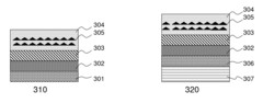
- A method involving the deposition of semiconductor layers with predetermined stress and strain profiles on a host substrate, followed by patterning and selective etching to form rolled-up micro- and nanotubes, allowing for the incorporation of quantum dots and precise transfer of these tubes onto foreign substrates like silicon for integration with CMOS chips, enabling low-stress and high-quality device fabrication.
Environmental Impact of Silicon Micropillar Production
The production of silicon micropillars for advanced optomechanical applications has significant environmental implications that warrant careful consideration. The manufacturing process involves several stages, each with its own environmental impact. The primary raw material, silicon, is typically sourced from silica sand, which requires energy-intensive mining and refining processes. These activities can lead to habitat disruption, soil erosion, and water pollution in mining areas.
The fabrication of silicon micropillars often employs techniques such as photolithography and etching, which involve the use of various chemicals and gases. Many of these substances, including photoresists, developers, and etchants, can be hazardous if not properly managed. Proper disposal and treatment of these chemicals are crucial to prevent contamination of soil and water resources. Additionally, the clean room environments required for micropillar production consume substantial amounts of energy for maintaining precise temperature, humidity, and air quality conditions.
Water usage is another significant environmental concern in silicon micropillar production. The manufacturing process requires large volumes of ultra-pure water for cleaning and rinsing steps. The purification and subsequent treatment of this water contribute to the overall environmental footprint of the production process. Furthermore, the high energy demands of silicon micropillar fabrication often rely on fossil fuel-based power sources, contributing to greenhouse gas emissions and climate change.
The production of silicon micropillars also generates various forms of waste, including silicon wafer scraps, used chemicals, and contaminated materials. Proper recycling and disposal of these wastes are essential to minimize environmental impact. Some manufacturers have implemented recycling programs for silicon wafers and other materials, but challenges remain in achieving fully circular production processes.
On the positive side, the advanced optomechanical applications enabled by silicon micropillars can contribute to environmental benefits in other sectors. For instance, improved optical sensors and communication devices can enhance energy efficiency in various industries, potentially offsetting some of the environmental costs of production. Additionally, ongoing research into more sustainable manufacturing techniques, such as bio-inspired fabrication methods and green chemistry approaches, shows promise in reducing the environmental impact of silicon micropillar production in the future.
As the demand for silicon micropillars in optomechanical applications continues to grow, it is crucial for manufacturers and researchers to prioritize environmentally friendly production methods. This includes developing more efficient fabrication processes, increasing the use of renewable energy sources, implementing comprehensive recycling programs, and exploring alternative materials with lower environmental impacts. Balancing the technological benefits of silicon micropillars with their environmental costs will be key to ensuring sustainable development in this field.
Standardization Efforts in Optomechanical Applications
In the rapidly evolving field of optomechanical applications, standardization efforts have become increasingly crucial to ensure interoperability, reliability, and consistency across various systems and devices. These efforts are particularly significant in the context of silicon micropillars, which have emerged as a key component in advanced optomechanical applications.
Several international organizations and industry consortia have been actively working towards establishing standards for optomechanical systems. The International Organization for Standardization (ISO) has formed a technical committee dedicated to optics and photonics, which includes a working group focused on optomechanical components and systems. This group is developing standards for terminology, testing methods, and performance specifications for optomechanical devices, including those incorporating silicon micropillars.
The Institute of Electrical and Electronics Engineers (IEEE) has also been contributing to standardization efforts in this field. Their Photonics Society has established a task force on optomechanical systems, which aims to create guidelines for the design, fabrication, and characterization of optomechanical components, with a particular emphasis on emerging technologies like silicon micropillars.
In the United States, the National Institute of Standards and Technology (NIST) has been actively involved in developing measurement standards and calibration techniques for optomechanical systems. Their work includes the creation of reference materials and standardized testing procedures for silicon micropillars used in optomechanical applications.
The European Committee for Standardization (CEN) has also recognized the importance of optomechanical standardization. They have initiated a project to develop European standards for optomechanical components, which includes specifications for silicon micropillars and their integration into larger systems.
Industry-led initiatives have also played a significant role in standardization efforts. The Optoelectronics Industry Development Association (OIDA) has formed a working group focused on optomechanical standards, bringing together key players from academia and industry to collaborate on developing best practices and guidelines for the design and manufacture of optomechanical components.
These standardization efforts are expected to have a profound impact on the future development and adoption of silicon micropillars in advanced optomechanical applications. By establishing common terminology, measurement techniques, and performance criteria, these standards will facilitate better communication between researchers, manufacturers, and end-users. This, in turn, will accelerate innovation, improve product quality, and reduce costs associated with the development and implementation of optomechanical systems.
As the field continues to advance, it is anticipated that standardization efforts will evolve to address new challenges and opportunities presented by emerging technologies. This ongoing process will be crucial in ensuring that silicon micropillars and other optomechanical components can be effectively integrated into a wide range of applications, from telecommunications to quantum computing.
Unlock deeper insights with Patsnap Eureka Quick Research — get a full tech report to explore trends and direct your research. Try now!
Generate Your Research Report Instantly with AI Agent
Supercharge your innovation with Patsnap Eureka AI Agent Platform!