Silicon Micropillars for Improved Optical Communication
JUL 9, 20259 MIN READ
Generate Your Research Report Instantly with AI Agent
Patsnap Eureka helps you evaluate technical feasibility & market potential.
Silicon Micropillars Background and Objectives
Silicon micropillars have emerged as a promising technology in the field of optical communication, offering potential solutions to the ever-increasing demand for faster and more efficient data transmission. The development of silicon micropillars can be traced back to the early 2000s when researchers began exploring ways to enhance the performance of silicon-based photonic devices. This technology leverages the unique properties of silicon, a material that has long been the cornerstone of the semiconductor industry, to create structures that can manipulate light at the microscale.
The primary objective of research on silicon micropillars for improved optical communication is to overcome the limitations of traditional optical components and pave the way for next-generation photonic integrated circuits. These micropillars, typically ranging from a few hundred nanometers to several micrometers in height, are designed to enhance light-matter interactions, improve light confinement, and facilitate efficient coupling between optical and electronic components.
One of the key goals in this field is to achieve higher data transmission rates while reducing power consumption. Silicon micropillars offer the potential to create compact, high-performance optical modulators, detectors, and waveguides that can operate at speeds exceeding 100 Gbps. Additionally, researchers aim to develop micropillar-based structures that can support wavelength division multiplexing (WDM) techniques, allowing for the simultaneous transmission of multiple data streams on different wavelengths.
Another critical objective is to improve the integration of optical components with existing CMOS (Complementary Metal-Oxide-Semiconductor) technology. Silicon micropillars provide a promising avenue for bridging the gap between photonics and electronics, potentially leading to the development of hybrid optoelectronic devices that combine the best of both worlds. This integration could revolutionize data centers, telecommunications networks, and high-performance computing systems.
The research on silicon micropillars also aims to address the challenges of optical signal loss and dispersion in long-distance communication. By engineering the geometry and arrangement of micropillars, scientists seek to create structures that can guide light with minimal losses and compensate for signal degradation over extended distances. This could lead to more efficient and reliable long-haul optical networks.
As the field progresses, there is a growing focus on exploring novel fabrication techniques to produce silicon micropillars with precise dimensions and optimal optical properties. Advanced lithography methods, etching processes, and self-assembly techniques are being investigated to create large-scale, uniform arrays of micropillars with tailored characteristics. The ultimate goal is to develop scalable manufacturing processes that can bring silicon micropillar-based devices from the laboratory to commercial production.
Optical Communication Market Analysis
The optical communication market has experienced significant growth in recent years, driven by the increasing demand for high-speed data transmission and the expansion of telecommunications networks. This market encompasses various components, including transceivers, optical fibers, and related equipment, with silicon micropillars emerging as a promising technology for improving optical communication performance.
The global optical communication market was valued at approximately $18.9 billion in 2020 and is projected to reach $27.8 billion by 2025, growing at a compound annual growth rate (CAGR) of 8.1%. This growth is primarily attributed to the rising adoption of cloud-based services, the proliferation of data centers, and the ongoing deployment of 5G networks worldwide.
Key market segments within optical communication include enterprise, telecom, data center, and others. The enterprise segment currently holds the largest market share, driven by the increasing need for high-speed connectivity in corporate environments. However, the data center segment is expected to witness the highest growth rate due to the rapid expansion of cloud computing and the Internet of Things (IoT).
Geographically, North America dominates the optical communication market, followed by Europe and Asia-Pacific. The Asia-Pacific region is anticipated to experience the fastest growth, fueled by extensive investments in telecommunications infrastructure and the rapid digitalization of emerging economies such as China and India.
The market for silicon micropillars in optical communication is still in its nascent stage but shows promising potential. As research progresses, silicon micropillars are expected to play a crucial role in enhancing the efficiency and performance of optical communication systems. This technology could potentially address key challenges in the industry, such as reducing power consumption, increasing data transmission rates, and improving signal integrity.
Several factors are driving the demand for improved optical communication technologies, including the exponential growth of internet traffic, the need for higher bandwidth in data centers, and the increasing adoption of cloud-based services. Additionally, the ongoing transition to 5G and future 6G networks is expected to further boost the demand for advanced optical communication solutions.
However, the market also faces certain challenges, such as high initial investment costs and the complexity of integrating new technologies into existing infrastructure. Despite these obstacles, the potential benefits of silicon micropillars and other emerging technologies are likely to drive continued investment and innovation in the optical communication market.
Silicon Micropillars: Current State and Challenges
Silicon micropillars have emerged as a promising technology for enhancing optical communication systems. The current state of this technology is characterized by significant advancements in fabrication techniques and performance optimization. However, several challenges remain in fully realizing the potential of silicon micropillars for improved optical communication.
One of the primary achievements in the field is the development of high-precision fabrication methods for creating silicon micropillars with controlled dimensions and spacing. Techniques such as electron beam lithography and deep reactive ion etching have enabled the production of micropillars with diameters ranging from a few hundred nanometers to several micrometers. These advancements have led to improved light confinement and manipulation capabilities, crucial for enhancing optical communication efficiency.
Despite these achievements, researchers face challenges in achieving uniform micropillar arrays over large areas, which is essential for practical applications in optical communication devices. Variations in pillar height, diameter, and spacing can lead to inconsistent optical properties across the array, potentially degrading overall performance.
Another significant development is the integration of silicon micropillars with other photonic components, such as waveguides and resonators. This integration has paved the way for more compact and efficient optical communication systems. However, challenges persist in optimizing the coupling efficiency between micropillars and other components, as well as minimizing losses at these interfaces.
The current state of silicon micropillar technology also includes efforts to enhance their light-emitting properties. While silicon is an indirect bandgap material and inherently a poor light emitter, researchers have made progress in overcoming this limitation through various strategies, such as strain engineering and doping. Nevertheless, achieving high-efficiency light emission from silicon micropillars remains a significant challenge, particularly when compared to III-V semiconductor materials.
Thermal management is another critical challenge in the development of silicon micropillar-based optical communication systems. As device densities increase and optical power levels rise, managing heat dissipation becomes crucial to maintain stable performance and prevent device degradation. Innovative cooling strategies and thermal design considerations are actively being explored to address this issue.
Furthermore, the current state of silicon micropillar technology faces challenges in terms of scalability and cost-effectiveness for mass production. While laboratory-scale demonstrations have shown promising results, transitioning these technologies to large-scale manufacturing processes while maintaining performance and yield remains a significant hurdle.
In conclusion, while silicon micropillars have shown great potential for improving optical communication, the technology is still evolving. Overcoming challenges in fabrication uniformity, integration, light emission efficiency, thermal management, and scalability will be crucial for realizing the full potential of silicon micropillars in next-generation optical communication systems.
Existing Silicon Micropillar Fabrication Techniques
01 Silicon micropillar structures for optical communication
Silicon micropillars are used in optical communication systems to enhance light transmission and manipulation. These structures can be designed to guide, focus, or modulate light signals, improving the efficiency and performance of optical communication devices.- Silicon micropillar structures for optical communication: Silicon micropillars are used in optical communication systems to enhance light transmission and manipulation. These structures can be designed to guide, focus, or modulate light signals, improving the efficiency and performance of optical communication devices.
- Integration of silicon micropillars with photonic devices: Silicon micropillars can be integrated with various photonic devices such as waveguides, resonators, and modulators. This integration allows for the creation of compact and efficient optical communication components, enabling high-speed data transmission and processing.
- Fabrication techniques for silicon micropillars: Advanced fabrication techniques are employed to create silicon micropillars for optical communication applications. These may include lithography, etching, and deposition processes to achieve precise control over the size, shape, and arrangement of the micropillars, optimizing their optical properties.
- Silicon micropillars for optical signal processing: Silicon micropillars can be utilized for various optical signal processing functions in communication systems. These may include filtering, multiplexing, demultiplexing, and switching of optical signals, enhancing the overall performance and flexibility of optical networks.
- Silicon micropillars in optical interconnects: Silicon micropillars play a crucial role in optical interconnects, facilitating high-speed data transmission between chips, boards, or systems. They can be designed to efficiently couple light between different components, reducing signal loss and improving communication bandwidth in complex optical networks.
02 Integration of silicon micropillars with optical fibers
Silicon micropillars can be integrated with optical fibers to create advanced optical communication systems. This integration allows for efficient coupling between the micropillars and fibers, enabling improved signal transmission and reception in optical networks.Expand Specific Solutions03 Fabrication techniques for silicon micropillars
Various fabrication techniques are employed to create silicon micropillars for optical communication applications. These may include lithography, etching, and deposition processes to achieve precise control over the size, shape, and arrangement of the micropillars.Expand Specific Solutions04 Silicon micropillars in photonic integrated circuits
Silicon micropillars are incorporated into photonic integrated circuits to enhance their functionality in optical communication systems. These structures can be used to create on-chip optical components such as waveguides, resonators, and modulators.Expand Specific Solutions05 Applications of silicon micropillars in optical switches and routers
Silicon micropillars are utilized in the development of optical switches and routers for advanced optical communication networks. These structures enable the creation of compact, high-performance devices capable of routing and switching optical signals with low loss and high speed.Expand Specific Solutions
Key Players in Silicon Micropillars Research
The research on silicon micropillars for improved optical communication is in a nascent stage, with the market still developing. The technology's potential to enhance optical communication systems has attracted interest from both academia and industry. Key players like NEC Corp., GlobalFoundries, and Intel Corp. are investing in this area, leveraging their semiconductor expertise. Universities such as Zhejiang University and Nanyang Technological University are contributing to fundamental research. The market size is expected to grow as the technology matures and finds applications in data centers and telecommunications. However, challenges in scalability and integration with existing systems need to be addressed before widespread adoption can occur.
Corning, Inc.
Technical Solution: Corning has focused on developing silicon micropillar technology for improved optical fiber-to-chip coupling. Their approach involves creating tapered silicon micropillar arrays on the chip surface to act as mode size converters between optical fibers and on-chip waveguides. Corning's micropillars are fabricated using a combination of lithography and etching techniques, with heights ranging from 10 to 50 μm and tip diameters as small as 200 nm [9]. The company has demonstrated coupling efficiencies exceeding 90% across a wide wavelength range, making the technology suitable for wavelength division multiplexing (WDM) systems. Corning has also explored the use of these micropillars in creating compact, high-performance optical sensors for various applications [10].
Strengths: High coupling efficiency across a wide wavelength range and potential for compact optical sensor applications. Weaknesses: Potential fragility of fine micropillar structures and challenges in mass production of consistent arrays.
Intel Corp.
Technical Solution: Intel has developed advanced silicon micropillar technology for improved optical communication. Their approach involves creating high-aspect-ratio silicon pillars with diameters ranging from 50 to 200 nm and heights up to several micrometers [1]. These pillars are fabricated using deep reactive ion etching (DRIE) and can be integrated with existing CMOS processes. Intel's silicon micropillars enhance light coupling efficiency and reduce optical losses in chip-to-chip and on-chip communication systems. The company has also explored the use of these micropillars in silicon photonics platforms, enabling higher bandwidth and lower power consumption in data centers and high-performance computing applications [3].
Strengths: Seamless integration with existing CMOS processes, improved light coupling efficiency, and reduced optical losses. Weaknesses: Potential challenges in mass production and maintaining consistent pillar quality across large wafers.
Core Innovations in Silicon Micropillar Design
Silicon nitride waveguide coupled photodiode
PatentActiveUS20240105875A1
Innovation
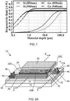
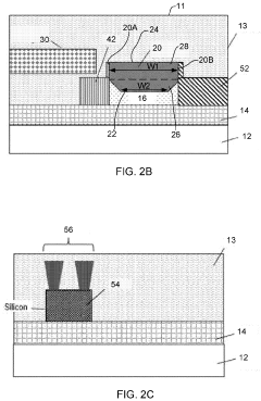
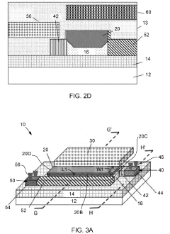
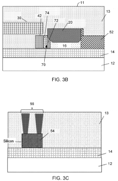
- A silicon nitride waveguide coupled Ge-on-Si photodiode structure is developed, featuring a germanium absorption region with a specific cross-sectional shape, a PIN or SACM configuration, and a silicon nitride waveguide to enhance light coupling and responsivity in the specified wavelength range.
Direct-bonded optoelectronic interconnect for high-density integrated photonics
PatentWO2019118846A1
Innovation
- Direct-bonded optoelectronic interconnects enable the integration of fully-processed III-V semiconductor devices onto silicon or SOI wafers using adhesive-free dielectric-to-dielectric and solder-free metal-to-metal bonding, allowing for simultaneous optical and electrical interconnects on a single interface, enabling high-density integration and precise photolithography.
Integration Challenges in Optical Systems
The integration of silicon micropillars into optical communication systems presents several significant challenges that must be addressed to fully realize their potential for improved performance. One of the primary obstacles is the precise alignment and coupling of these micropillars with existing optical components. The nanoscale dimensions of silicon micropillars require extremely accurate positioning to ensure optimal light transmission and minimal signal loss.
Another critical challenge lies in the fabrication process of these micropillars. Achieving consistent and uniform structures across large arrays is essential for reliable system performance. Current manufacturing techniques often struggle to maintain the necessary precision over large areas, leading to variations in pillar height, diameter, and spacing. These inconsistencies can result in unpredictable optical properties and reduced overall system efficiency.
Thermal management is a significant concern in the integration of silicon micropillars. As optical systems become more compact and powerful, heat dissipation becomes increasingly problematic. Silicon micropillars, due to their high surface area-to-volume ratio, can potentially exacerbate thermal issues if not properly managed. Developing effective cooling strategies that do not interfere with the optical properties of the micropillars is crucial for long-term system stability and performance.
The interface between silicon micropillars and other materials in the optical system poses another integration challenge. Ensuring seamless transitions between different components, such as waveguides, detectors, and light sources, is critical for minimizing signal loss and maintaining high-quality optical transmission. This often requires the development of novel interface materials and techniques that can accommodate the unique properties of silicon micropillars while maintaining compatibility with existing optical technologies.
Scalability is a key consideration in the integration of silicon micropillars into practical optical communication systems. While promising results have been demonstrated in laboratory settings, translating these achievements to large-scale, commercially viable production remains a significant hurdle. Developing manufacturing processes that can reliably produce high-quality micropillar arrays at scale, while maintaining cost-effectiveness, is essential for widespread adoption of this technology.
Lastly, the long-term reliability and durability of silicon micropillar-based optical systems must be carefully evaluated. Factors such as environmental stability, resistance to degradation over time, and compatibility with standard packaging and protection methods need to be thoroughly addressed to ensure that these systems can meet the rigorous demands of real-world optical communication applications.
Environmental Impact of Silicon Micropillar Production
The production of silicon micropillars for improved optical communication has significant environmental implications that warrant careful consideration. The manufacturing process involves several stages, each with its own environmental impact. Firstly, the extraction and purification of silicon from raw materials require substantial energy inputs and can lead to habitat disruption in mining areas. The subsequent fabrication of micropillars often employs chemical etching techniques, which may generate hazardous waste products if not properly managed.
The use of cleanroom facilities, essential for the precise manufacturing of silicon micropillars, contributes to high energy consumption and the potential release of greenhouse gases. These facilities require stringent environmental controls, including air filtration and temperature regulation, which are energy-intensive processes. Additionally, the production of specialized equipment and materials used in micropillar fabrication may involve the use of rare earth elements, further straining natural resources.
Water usage is another critical environmental concern in silicon micropillar production. The manufacturing process requires ultra-pure water for cleaning and processing, potentially leading to water scarcity issues in regions where production facilities are located. The disposal of wastewater from these processes must be carefully managed to prevent contamination of local water sources.
On the positive side, the improved efficiency of optical communication systems enabled by silicon micropillars could lead to reduced energy consumption in data transmission over the long term. This potential energy saving may partially offset the environmental costs of production. Furthermore, the miniaturization of components facilitated by micropillar technology could result in smaller devices, potentially reducing material usage and electronic waste.
The lifecycle assessment of silicon micropillars must also consider end-of-life disposal. While silicon is not inherently toxic, the complex nature of micropillar structures and potential contamination during use may complicate recycling efforts. Developing effective recycling methods for these components will be crucial in minimizing their long-term environmental impact.
To mitigate these environmental concerns, research into more sustainable production methods is essential. This includes exploring alternative materials, developing more efficient manufacturing processes, and implementing closed-loop systems for resource recovery. Additionally, industry-wide adoption of green chemistry principles and circular economy practices could significantly reduce the environmental footprint of silicon micropillar production.
Unlock deeper insights with Patsnap Eureka Quick Research — get a full tech report to explore trends and direct your research. Try now!
Generate Your Research Report Instantly with AI Agent
Supercharge your innovation with Patsnap Eureka AI Agent Platform!