How Silicon Micropillars Support LIDAR Technologies
JUL 9, 20259 MIN READ
Generate Your Research Report Instantly with AI Agent
Patsnap Eureka helps you evaluate technical feasibility & market potential.
LIDAR Tech Evolution
LIDAR (Light Detection and Ranging) technology has undergone significant evolution since its inception, with each advancement pushing the boundaries of its capabilities and applications. The journey of LIDAR began in the 1960s with simple distance measurements and has since transformed into a sophisticated 3D mapping and object detection system.
In the early stages, LIDAR systems were large, expensive, and primarily used for atmospheric studies and topographical mapping. The 1970s and 1980s saw the refinement of these systems, with improvements in laser technology and data processing capabilities. This period marked the beginning of LIDAR's use in autonomous vehicle research, albeit in a limited capacity due to the bulky nature of the equipment.
The 1990s brought about a revolution in LIDAR technology with the introduction of more compact and efficient systems. This decade saw the first practical applications of LIDAR in automotive safety features, such as adaptive cruise control. The miniaturization of components and advancements in semiconductor technology played a crucial role in this evolution.
The turn of the millennium heralded a new era for LIDAR, with the emergence of solid-state systems. These systems, which eliminated moving parts, significantly improved reliability and reduced costs. This development was pivotal in making LIDAR more accessible for a wider range of applications, including robotics and consumer electronics.
In recent years, the focus has shifted towards enhancing the resolution, range, and processing speed of LIDAR systems. The integration of artificial intelligence and machine learning algorithms has greatly improved the interpretation of LIDAR data, enabling more accurate and real-time decision-making in autonomous systems.
The introduction of silicon micropillars represents a cutting-edge development in LIDAR technology. These microscopic structures, typically arranged in arrays, offer several advantages over traditional LIDAR components. Silicon micropillars can be precisely engineered to manipulate light in ways that enhance the performance of LIDAR systems, including improved beam steering, increased sensitivity, and reduced signal noise.
The use of silicon micropillars in LIDAR technology marks a significant step towards more compact, efficient, and cost-effective systems. This innovation aligns with the broader trend of miniaturization and integration in the semiconductor industry, potentially leading to LIDAR sensors that are small enough to be embedded in everyday devices.
As LIDAR technology continues to evolve, we can expect further improvements in resolution, range, and processing capabilities. The ongoing research into novel materials and fabrication techniques, including the refinement of silicon micropillar technology, promises to unlock new possibilities for LIDAR applications across various industries, from autonomous vehicles to smart cities and environmental monitoring.
Market Demand Analysis
The market demand for LiDAR technologies supported by silicon micropillars has been experiencing significant growth, driven by the rapid expansion of autonomous vehicles, advanced driver assistance systems (ADAS), and smart city applications. As these sectors continue to evolve, the need for more efficient, compact, and cost-effective LiDAR solutions has become paramount, positioning silicon micropillar-based technologies at the forefront of innovation.
In the automotive industry, which represents the largest market segment for LiDAR technologies, the demand is primarily fueled by the push towards higher levels of vehicle autonomy. Major automakers and tech companies are investing heavily in self-driving technology, creating a robust market for advanced LiDAR systems. The integration of silicon micropillars in LiDAR design offers the potential for improved performance and reduced costs, aligning with the industry's goals of making autonomous vehicles more accessible and reliable.
Beyond automotive applications, the smart city sector is emerging as a significant driver of LiDAR demand. Urban planners and governments are increasingly adopting LiDAR technologies for traffic management, infrastructure monitoring, and environmental sensing. Silicon micropillar-based LiDAR systems, with their potential for miniaturization and enhanced efficiency, are well-positioned to meet the diverse needs of smart city initiatives.
The industrial automation sector also presents a growing market for advanced LiDAR technologies. As factories and warehouses become more automated, the demand for precise 3D sensing and object detection capabilities is rising. Silicon micropillar LiDAR systems offer the potential for improved accuracy and reliability in these challenging environments, driving adoption across various industrial applications.
Market analysts project the global LiDAR market to grow at a compound annual growth rate (CAGR) of over 20% in the coming years. While traditional LiDAR technologies currently dominate the market, silicon micropillar-based solutions are expected to gain significant market share due to their potential advantages in size, cost, and performance.
The increasing focus on environmental monitoring and disaster management has also contributed to the expanding market for LiDAR technologies. Silicon micropillar-based systems, with their potential for improved resolution and efficiency, are well-suited for applications such as forest management, coastal erosion monitoring, and natural disaster risk assessment.
As the demand for more sophisticated and miniaturized LiDAR solutions continues to grow across various sectors, the market for silicon micropillar-supported technologies is poised for substantial expansion. The ability of these technologies to address key industry challenges, such as size reduction, cost-effectiveness, and performance enhancement, positions them as a critical component in the future of LiDAR applications.
Silicon Micropillars
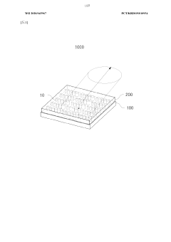
Silicon micropillars represent a groundbreaking advancement in the field of Light Detection and Ranging (LIDAR) technologies. These microscopic structures, typically fabricated from silicon, play a crucial role in enhancing the performance and efficiency of LIDAR systems. The integration of silicon micropillars into LIDAR devices has opened up new possibilities for improved sensing capabilities and miniaturization.
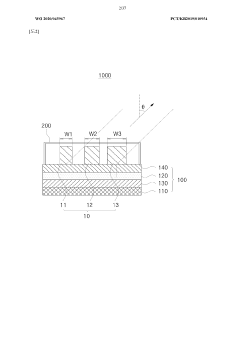
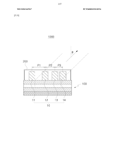
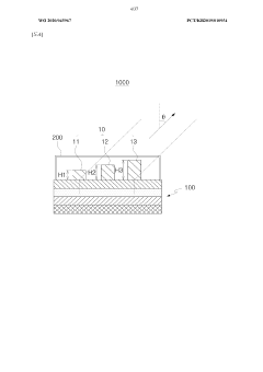
At their core, silicon micropillars are vertically oriented, high-aspect-ratio structures with dimensions in the micrometer range. Their unique geometry and material properties make them ideal for manipulating light at the microscale, which is essential for LIDAR applications. The ability to precisely control the size, shape, and spacing of these micropillars allows for fine-tuning of their optical properties, enabling enhanced light emission, detection, and waveguiding.
One of the primary ways silicon micropillars support LIDAR technologies is through their role in beam steering and focusing. By arranging micropillars in specific patterns, it becomes possible to create metasurfaces that can dynamically control the direction and shape of light beams. This capability is crucial for LIDAR systems, as it allows for rapid and precise scanning of the environment without the need for bulky mechanical components.
Furthermore, silicon micropillars contribute to improved light collection efficiency in LIDAR sensors. Their high surface-to-volume ratio and ability to trap light through multiple internal reflections significantly enhance the absorption of incoming photons. This increased sensitivity translates to better detection of weak signals from distant or low-reflectivity objects, ultimately expanding the range and accuracy of LIDAR systems.
The integration of silicon micropillars also enables the development of more compact and energy-efficient LIDAR devices. By leveraging the unique properties of these structures, researchers have been able to reduce the overall size of LIDAR components while maintaining or even improving performance. This miniaturization is particularly valuable for applications in autonomous vehicles, drones, and portable sensing devices, where space and power consumption are critical factors.
Additionally, silicon micropillars offer advantages in terms of manufacturability and scalability. The well-established silicon fabrication processes in the semiconductor industry can be adapted to produce these structures with high precision and consistency. This compatibility with existing manufacturing techniques facilitates the integration of micropillar-based LIDAR components into larger systems and paves the way for cost-effective mass production.
As research in this field continues to advance, silicon micropillars are expected to play an increasingly important role in pushing the boundaries of LIDAR technology. Their versatility and potential for further optimization make them a promising platform for addressing current limitations in LIDAR systems and enabling new applications across various industries.
Current Micropillar
01 Fabrication methods for silicon micropillars
Various techniques are employed to create silicon micropillars, including etching processes, lithography, and deposition methods. These fabrication methods allow for precise control over the size, shape, and arrangement of the micropillars, which is crucial for their performance in different applications.- Fabrication methods for silicon micropillars: Various techniques are employed to create silicon micropillars, including etching processes, lithography, and deposition methods. These fabrication methods allow for precise control over the size, shape, and arrangement of the micropillars, which is crucial for their performance in different applications.
- Applications in solar cells and photovoltaics: Silicon micropillars are utilized in solar cell and photovoltaic technologies to enhance light absorption and improve overall efficiency. The unique structure of micropillars allows for better light trapping and increased surface area, leading to improved energy conversion rates.
- Use in microfluidic and lab-on-a-chip devices: Silicon micropillars play a significant role in microfluidic systems and lab-on-a-chip devices. They can be used for fluid manipulation, particle separation, and as support structures for various biochemical processes, enhancing the functionality and efficiency of these miniaturized systems.
- Integration with MEMS and sensor technologies: Silicon micropillars are integrated into Micro-Electro-Mechanical Systems (MEMS) and various sensor technologies. Their unique properties allow for the development of highly sensitive and precise sensors for applications in environmental monitoring, biomedical devices, and industrial process control.
- Surface modification and functionalization: The surface of silicon micropillars can be modified and functionalized to enhance their properties or add new functionalities. This includes coating with various materials, chemical treatments, or the addition of specific molecules to tailor the micropillars for specific applications such as biosensing or catalysis.
02 Applications in solar cells and photovoltaics
Silicon micropillars are utilized in solar cell and photovoltaic technologies to enhance light absorption and improve overall efficiency. The unique structure of micropillars allows for better light trapping and increased surface area, leading to improved energy conversion in solar devices.Expand Specific Solutions03 Use in microfluidic and lab-on-a-chip devices
Silicon micropillars play a significant role in microfluidic systems and lab-on-a-chip devices. They can be used for fluid manipulation, particle separation, and as structural elements in miniaturized analytical systems, enabling more efficient and precise microfluidic operations.Expand Specific Solutions04 Integration with sensors and MEMS devices
Silicon micropillars are integrated into various sensors and MEMS (Micro-Electro-Mechanical Systems) devices. Their unique properties allow for enhanced sensitivity in chemical and biological sensors, as well as improved performance in mechanical sensing applications.Expand Specific Solutions05 Surface modification and functionalization
The surface of silicon micropillars can be modified and functionalized to tailor their properties for specific applications. This includes coating with various materials, chemical treatments, and the addition of functional groups to enhance their performance in areas such as catalysis, sensing, and biomedical applications.Expand Specific Solutions
Key LIDAR Players
The market for silicon micropillars in LIDAR technologies is in a growth phase, with increasing demand driven by autonomous vehicles and other sensing applications. The global LIDAR market size is projected to reach several billion dollars by 2025. While the technology is advancing rapidly, it is still evolving towards full maturity. Key players like RoboSense, Aurora, and SOS LAB are developing innovative LIDAR solutions incorporating silicon micropillars. Established companies such as Osram and Sony Semiconductor Solutions are also active in this space, leveraging their expertise in optoelectronics. The competitive landscape is dynamic, with both startups and large corporations vying for market share through technological advancements and strategic partnerships.
MicroVision, Inc.
Technical Solution: MicroVision has developed a proprietary MEMS-based LiDAR technology that utilizes silicon micropillars to enhance the performance and efficiency of their LiDAR systems. Their approach involves creating an array of microscopic silicon pillars on a single chip, which acts as both the emitter and receiver for laser light. This design allows for a more compact and cost-effective LiDAR solution. The silicon micropillars are precisely engineered to manipulate the laser light, improving beam steering capabilities and increasing the overall resolution of the LiDAR system[1][3]. MicroVision's technology also incorporates advanced signal processing algorithms that work in conjunction with the silicon micropillar array to filter out noise and enhance the accuracy of distance measurements[2].
Strengths: Compact design, improved resolution, and cost-effectiveness. Weaknesses: May face challenges in scaling production and competing with established LiDAR manufacturers.
SiLC Technologies, Inc.
Technical Solution: SiLC Technologies has developed a silicon photonics-based LiDAR solution that leverages silicon micropillars to enhance the performance of their 4D+ Vision Chip. Their approach integrates the entire LiDAR system, including laser, detector, and processing units, onto a single chip. The silicon micropillars are used to create optical waveguides and resonators, which help in manipulating and directing the laser light with high precision. This integration allows for a significant reduction in size, power consumption, and cost compared to traditional LiDAR systems[4]. SiLC's technology also incorporates frequency-modulated continuous-wave (FMCW) LiDAR techniques, which provide additional benefits such as instantaneous velocity measurements and improved performance in adverse weather conditions[5].
Strengths: Highly integrated solution, low power consumption, and advanced FMCW capabilities. Weaknesses: May face challenges in achieving long-range performance comparable to discrete LiDAR systems.
Core Micropillar Tech
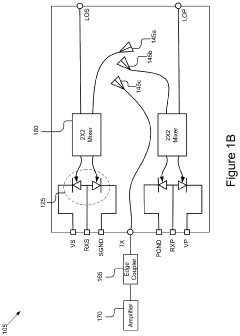
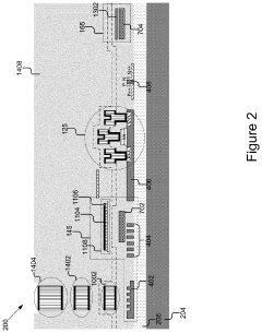
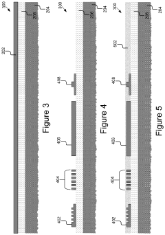
Silicon Photonics Device for LIDAR Sensor and Method for Fabrication
PatentActiveUS20240151820A1
Innovation
- A silicon photonics device with a one-dimensional grating coupler antenna and a photodiode is developed, featuring a substrate with specific dielectric and metal layer structures, along with a diffusion barrier and adhesion layer to enhance coupling efficiency, and a method for fabrication that includes forming insulating structures and metal layers to improve performance.
Lidar device
PatentWO2020045967A1
Innovation
- The use of VCSEL elements and metasurfaces with nanopillars to steer laser beams, forming sub-wavelength patterns that enable miniaturization and 3D scanning by distributing scanning points in arrays, allowing for precise distance measurement and beam steering.
Manufacturing Process
The manufacturing process of silicon micropillars for LIDAR technologies involves a series of precise and sophisticated steps. The process typically begins with the selection of high-quality silicon wafers as the base material. These wafers undergo thorough cleaning and preparation to ensure a pristine surface for subsequent processing.
The next crucial step is photolithography, where a photoresist layer is applied to the silicon wafer. This layer is then exposed to ultraviolet light through a mask that defines the desired micropillar pattern. The exposed areas of the photoresist are chemically altered, allowing for selective removal in the development process.
Following photolithography, etching techniques are employed to create the micropillar structures. Deep Reactive Ion Etching (DRIE) is a commonly used method, offering high aspect ratio and precise control over pillar dimensions. This process involves alternating etching and passivation steps to achieve vertical sidewalls and the desired pillar height.
Post-etching, the wafers undergo a series of cleaning and inspection steps to remove any residual materials and ensure the quality of the micropillars. Advanced metrology techniques, such as scanning electron microscopy (SEM) and atomic force microscopy (AFM), are used to verify the dimensions and surface characteristics of the micropillars.
In some cases, additional surface treatments may be applied to enhance the optical properties of the micropillars. These treatments can include oxidation, deposition of anti-reflective coatings, or functionalization with specific materials to improve light interaction and detection efficiency.
The final stages of the manufacturing process involve dicing the wafer into individual chips and packaging them for integration into LIDAR systems. This step requires precision handling to prevent damage to the delicate micropillar structures.
Throughout the entire manufacturing process, strict quality control measures are implemented to ensure consistency and reliability. Environmental factors such as temperature, humidity, and cleanliness are carefully controlled to minimize defects and optimize yield.
The manufacturing of silicon micropillars for LIDAR applications demands a high level of expertise and specialized equipment. Continuous advancements in fabrication techniques and materials science contribute to improving the performance and cost-effectiveness of these critical components in LIDAR technologies.
Environmental Impact
The integration of silicon micropillars in LIDAR technologies brings significant environmental considerations to the forefront. These structures, while enhancing the performance and efficiency of LIDAR systems, also present both positive and negative environmental impacts that warrant careful examination.
On the positive side, silicon micropillars contribute to the miniaturization of LIDAR devices, potentially reducing the overall material consumption in their production. This downsizing effect can lead to a decrease in the environmental footprint associated with manufacturing processes, transportation, and eventual disposal of LIDAR equipment. Furthermore, the improved efficiency of LIDAR systems supported by silicon micropillars may result in reduced power consumption, indirectly lowering the carbon emissions linked to the operation of these devices.
However, the production of silicon micropillars involves complex manufacturing processes that may require specialized equipment and potentially harmful chemicals. The environmental impact of these production methods, including energy consumption and waste generation, needs to be carefully assessed and mitigated. Additionally, the increased use of silicon in LIDAR technologies raises concerns about the sustainability of silicon sourcing and the potential environmental degradation associated with silicon mining and processing.
The durability and longevity of silicon micropillar-enhanced LIDAR systems also play a crucial role in their environmental impact. If these advanced structures contribute to extended product lifespans, they could significantly reduce electronic waste generation. Conversely, if the intricate nature of these components makes repairs or recycling more challenging, it could exacerbate e-waste issues.
In the context of LIDAR applications, particularly in autonomous vehicles and environmental monitoring, silicon micropillars can indirectly contribute to positive environmental outcomes. By enabling more accurate and efficient sensing capabilities, these technologies can optimize route planning, reduce traffic congestion, and improve overall energy efficiency in transportation systems. In environmental monitoring applications, enhanced LIDAR performance can lead to more precise data collection, potentially aiding in conservation efforts and climate change research.
As the adoption of silicon micropillar-supported LIDAR technologies grows, it becomes imperative to develop comprehensive lifecycle assessments. These assessments should encompass the environmental impacts from raw material extraction to end-of-life disposal, ensuring a holistic understanding of the technology's ecological footprint. Furthermore, ongoing research into eco-friendly manufacturing processes and sustainable material alternatives for micropillars could help mitigate potential negative environmental effects while preserving the technological benefits.
Unlock deeper insights with Patsnap Eureka Quick Research — get a full tech report to explore trends and direct your research. Try now!
Generate Your Research Report Instantly with AI Agent
Supercharge your innovation with Patsnap Eureka AI Agent Platform!