Silicon Micropillars in Thermoelectric Applications
JUL 9, 20259 MIN READ
Generate Your Research Report Instantly with AI Agent
Patsnap Eureka helps you evaluate technical feasibility & market potential.
Thermoelectric Silicon Micropillars: Background and Objectives
Thermoelectric materials have garnered significant attention in recent years due to their potential to convert waste heat into useful electricity. Among these materials, silicon micropillars have emerged as a promising candidate for thermoelectric applications. The development of silicon micropillars for thermoelectric purposes represents a convergence of nanotechnology, materials science, and energy harvesting technologies.
The evolution of thermoelectric materials has been driven by the need for more efficient energy conversion systems. Traditional bulk thermoelectric materials have been limited by their relatively low efficiency, high cost, and environmental concerns. Silicon, being abundant, cost-effective, and environmentally friendly, has become an attractive alternative. The miniaturization of silicon structures into micropillars has opened up new possibilities for enhancing thermoelectric performance.
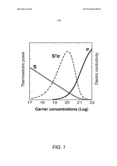
The primary objective of research on silicon micropillars in thermoelectric applications is to improve the figure of merit (ZT) of the material. ZT is a dimensionless quantity that determines the efficiency of a thermoelectric material. It is defined as ZT = S²σT/κ, where S is the Seebeck coefficient, σ is the electrical conductivity, T is the absolute temperature, and κ is the thermal conductivity. The challenge lies in simultaneously increasing the power factor (S²σ) while reducing thermal conductivity.
Silicon micropillars offer a unique approach to this challenge. By reducing the dimensionality of the material, quantum confinement effects can be exploited to enhance the Seebeck coefficient. Additionally, the increased surface area-to-volume ratio of micropillars can lead to increased phonon scattering, effectively reducing thermal conductivity without significantly impacting electrical conductivity.
The technological trajectory of silicon micropillars in thermoelectric applications has been marked by several key milestones. Initial research focused on understanding the fundamental physics of heat and charge transport in nanostructured silicon. This was followed by advancements in fabrication techniques, allowing for precise control over the size, shape, and arrangement of micropillars. Recent efforts have been directed towards optimizing doping profiles, surface treatments, and integration with other materials to further enhance thermoelectric performance.
Looking forward, the field aims to achieve practical implementation of silicon micropillar-based thermoelectric devices. This involves scaling up production, improving device stability and longevity, and developing efficient heat management systems. The ultimate goal is to create highly efficient, cost-effective thermoelectric generators that can be widely deployed for waste heat recovery in various industrial and consumer applications.
The evolution of thermoelectric materials has been driven by the need for more efficient energy conversion systems. Traditional bulk thermoelectric materials have been limited by their relatively low efficiency, high cost, and environmental concerns. Silicon, being abundant, cost-effective, and environmentally friendly, has become an attractive alternative. The miniaturization of silicon structures into micropillars has opened up new possibilities for enhancing thermoelectric performance.
The primary objective of research on silicon micropillars in thermoelectric applications is to improve the figure of merit (ZT) of the material. ZT is a dimensionless quantity that determines the efficiency of a thermoelectric material. It is defined as ZT = S²σT/κ, where S is the Seebeck coefficient, σ is the electrical conductivity, T is the absolute temperature, and κ is the thermal conductivity. The challenge lies in simultaneously increasing the power factor (S²σ) while reducing thermal conductivity.
Silicon micropillars offer a unique approach to this challenge. By reducing the dimensionality of the material, quantum confinement effects can be exploited to enhance the Seebeck coefficient. Additionally, the increased surface area-to-volume ratio of micropillars can lead to increased phonon scattering, effectively reducing thermal conductivity without significantly impacting electrical conductivity.
The technological trajectory of silicon micropillars in thermoelectric applications has been marked by several key milestones. Initial research focused on understanding the fundamental physics of heat and charge transport in nanostructured silicon. This was followed by advancements in fabrication techniques, allowing for precise control over the size, shape, and arrangement of micropillars. Recent efforts have been directed towards optimizing doping profiles, surface treatments, and integration with other materials to further enhance thermoelectric performance.
Looking forward, the field aims to achieve practical implementation of silicon micropillar-based thermoelectric devices. This involves scaling up production, improving device stability and longevity, and developing efficient heat management systems. The ultimate goal is to create highly efficient, cost-effective thermoelectric generators that can be widely deployed for waste heat recovery in various industrial and consumer applications.
Market Analysis for Thermoelectric Applications
The thermoelectric market has been experiencing significant growth in recent years, driven by increasing demand for energy-efficient technologies and sustainable power generation solutions. The global thermoelectric market size was valued at approximately $600 million in 2020 and is projected to reach over $1 billion by 2026, growing at a CAGR of around 8% during the forecast period.
Silicon micropillars have emerged as a promising technology in thermoelectric applications, offering potential advantages in terms of improved efficiency and cost-effectiveness. The market for silicon-based thermoelectric devices is expected to witness substantial growth, particularly in sectors such as automotive, aerospace, and consumer electronics.
In the automotive industry, thermoelectric generators utilizing silicon micropillars are gaining traction for waste heat recovery systems, contributing to improved fuel efficiency and reduced emissions. The increasing adoption of electric vehicles and the focus on energy management systems are further driving the demand for advanced thermoelectric solutions.
The consumer electronics sector presents another significant market opportunity for silicon micropillar-based thermoelectric devices. With the growing need for efficient cooling solutions in smartphones, laptops, and wearable devices, compact and high-performance thermoelectric modules are in high demand. Silicon micropillars offer the potential for miniaturization and integration, making them attractive for portable electronic applications.
The aerospace and defense sector is also showing interest in silicon micropillar thermoelectric technology for power generation in remote locations and space applications. The ability to convert waste heat into usable electricity aligns well with the industry's focus on energy efficiency and sustainability.
Geographically, North America and Asia-Pacific are expected to be the leading markets for silicon micropillar thermoelectric applications. The presence of major technology companies, research institutions, and government initiatives supporting clean energy technologies contribute to the market growth in these regions.
However, challenges such as high initial costs and the need for further improvements in conversion efficiency may hinder market growth to some extent. Ongoing research and development efforts are focused on addressing these challenges and enhancing the performance of silicon micropillar-based thermoelectric devices.
In conclusion, the market for silicon micropillars in thermoelectric applications shows promising growth potential across various industries. As technology advances and production costs decrease, wider adoption of these devices is expected, driving further market expansion in the coming years.
Current Challenges in Silicon Micropillar Technology
Silicon micropillar technology in thermoelectric applications faces several significant challenges that hinder its widespread adoption and commercialization. One of the primary obstacles is the difficulty in achieving precise control over the micropillar geometry and dimensions during fabrication. The performance of thermoelectric devices heavily relies on the size, shape, and spacing of these micropillars, making consistent and reproducible manufacturing a critical issue.
Another major challenge lies in the thermal and mechanical stability of silicon micropillars. When subjected to high temperatures and thermal cycling, these structures can undergo deformation or degradation, potentially compromising their thermoelectric properties and overall device performance. Addressing this issue requires the development of advanced materials and fabrication techniques that can enhance the resilience of silicon micropillars under extreme operating conditions.
The integration of silicon micropillars into practical thermoelectric devices presents additional complexities. Establishing reliable electrical and thermal contacts between the micropillars and other device components while maintaining low contact resistance is crucial for optimal performance. Furthermore, scaling up the production of silicon micropillar-based thermoelectric devices from laboratory prototypes to industrial-scale manufacturing remains a significant hurdle.
Heat management within silicon micropillar structures poses another challenge. Efficiently dissipating heat from the hot side of the device while maintaining a temperature gradient is essential for maximizing thermoelectric efficiency. Designing effective heat spreading mechanisms and optimizing the thermal conductivity of the overall structure are ongoing areas of research.
The cost-effectiveness of silicon micropillar technology is also a concern. Current fabrication methods, such as deep reactive ion etching (DRIE) or metal-assisted chemical etching (MACE), can be expensive and time-consuming when applied to large-scale production. Developing more economical and scalable manufacturing processes is crucial for the commercial viability of silicon micropillar-based thermoelectric devices.
Lastly, improving the overall thermoelectric figure of merit (ZT) of silicon micropillar structures remains a persistent challenge. While silicon micropillars have shown promise in enhancing thermoelectric properties compared to bulk silicon, further improvements in electrical conductivity, Seebeck coefficient, and thermal conductivity are necessary to compete with traditional thermoelectric materials. This requires ongoing research into novel doping strategies, surface treatments, and nanostructuring techniques to optimize the thermoelectric performance of silicon micropillars.
Existing Silicon Micropillar Fabrication Techniques
01 Fabrication methods for silicon micropillars
Various techniques are employed to create silicon micropillars, including etching processes, lithography, and deposition methods. These fabrication methods allow for precise control over the size, shape, and arrangement of the micropillars, which is crucial for their performance in different applications.- Fabrication methods for silicon micropillars: Various techniques are employed to create silicon micropillars, including etching processes, lithography, and deposition methods. These fabrication methods allow for precise control over the size, shape, and arrangement of the micropillars, which is crucial for their performance in different applications.
- Applications in solar cells and photovoltaics: Silicon micropillars are utilized in solar cell and photovoltaic technologies to enhance light absorption and improve overall efficiency. The unique structure of micropillars allows for better light trapping and increased surface area, leading to improved energy conversion in solar devices.
- Use in microfluidic and lab-on-a-chip devices: Silicon micropillars play a significant role in microfluidic systems and lab-on-a-chip devices. They can be used for fluid manipulation, particle separation, and as supports for biological assays, enhancing the functionality and efficiency of these miniaturized analytical platforms.
- Integration with electronic and sensing devices: Silicon micropillars are integrated into various electronic and sensing devices to improve their performance. They can enhance the sensitivity of sensors, act as electrodes in electronic components, and provide unique surface properties for specialized applications in fields such as bioelectronics and environmental monitoring.
- Surface modification and functionalization: The surface of silicon micropillars can be modified and functionalized to tailor their properties for specific applications. This includes coating with various materials, chemical treatments, and the addition of functional groups to enhance their performance in areas such as catalysis, sensing, and biomedical applications.
02 Applications in solar cells and photovoltaics
Silicon micropillars are utilized in solar cell and photovoltaic technologies to enhance light absorption and improve overall efficiency. The unique structure of micropillars allows for better light trapping and increased surface area, leading to improved energy conversion rates.Expand Specific Solutions03 Use in microfluidic devices and lab-on-a-chip systems
Silicon micropillars play a significant role in microfluidic devices and lab-on-a-chip systems. They can be used for fluid manipulation, particle separation, and as structural elements in miniaturized analytical systems, enabling more efficient and precise analysis in various fields.Expand Specific Solutions04 Integration with sensors and electronic devices
Silicon micropillars are integrated into various sensors and electronic devices to enhance their performance. They can be used to create high-sensitivity pressure sensors, improve thermal management in electronic components, and develop advanced MEMS (Micro-Electro-Mechanical Systems) devices.Expand Specific Solutions05 Surface modification and functionalization
The surface of silicon micropillars can be modified and functionalized to tailor their properties for specific applications. This includes coating with various materials, chemical treatments, and the addition of functional groups to enhance their performance in areas such as biosensing, catalysis, and water treatment.Expand Specific Solutions
Key Players in Thermoelectric Silicon Research
The research on silicon micropillars in thermoelectric applications is in an emerging phase, with significant potential for growth. The market size is expanding as demand for efficient energy harvesting solutions increases. Technologically, it's progressing from early-stage research to more advanced development, with key players like Stichting IMEC Nederland, Shanghai Institute of Microsystem & Information Technology, and California Institute of Technology leading innovation. Companies such as LONGi Green Energy Technology and Taiwan Semiconductor Manufacturing Co. are leveraging their semiconductor expertise to advance this field. The involvement of government agencies like the Japan Science & Technology Agency and academic institutions such as Harbin Institute of Technology indicates a collaborative approach to overcoming technical challenges and scaling up the technology for practical applications.
Stichting IMEC Nederland
Technical Solution: IMEC has developed advanced silicon micropillar structures for thermoelectric applications. Their approach involves creating highly ordered, vertically aligned silicon nanowires with precisely controlled dimensions and doping profiles. These micropillars are fabricated using a combination of deep reactive ion etching and selective epitaxial growth techniques, resulting in structures with diameters ranging from 50 to 200 nm and heights up to several micrometers[1]. The high aspect ratio and increased surface area of these micropillars significantly enhance phonon scattering, leading to reduced thermal conductivity while maintaining good electrical conductivity[2]. IMEC's research has demonstrated a figure of merit (ZT) improvement of up to 40% compared to bulk silicon at room temperature[3].
Strengths: High precision fabrication, improved thermoelectric efficiency, scalable manufacturing process. Weaknesses: Potential high production costs, challenges in maintaining structural integrity at larger scales.
California Institute of Technology
Technical Solution: Caltech's research on silicon micropillars for thermoelectric applications focuses on nanostructured silicon-based materials. Their approach involves creating arrays of silicon nanowires with diameters ranging from 20 to 300 nm using metal-assisted chemical etching techniques[4]. These nanowires are then treated with a thermal oxidation process to further reduce their thermal conductivity. Caltech researchers have reported a significant reduction in thermal conductivity, down to about 1.6 W/mK at room temperature, which is nearly two orders of magnitude lower than bulk silicon[5]. They have also explored the integration of these silicon micropillars with other materials, such as germanium, to create advanced heterostructures with enhanced thermoelectric properties[6].
Strengths: Dramatic reduction in thermal conductivity, potential for low-cost fabrication, compatibility with existing silicon-based technologies. Weaknesses: Challenges in maintaining electrical conductivity, potential fragility of nanostructures.
Innovative Designs for Enhanced Thermoelectric Performance
Nanostructured silicide composites for thermoelectric applications
PatentInactiveUS20140097391A1
Innovation
- A nanocomposite thermoelectric material is created by heating a reaction mixture of a semiconductor material and a metal complex to form metallic inclusions less than 100 nm in size, which are evenly distributed throughout the semiconductor, reducing lattice thermal conductivity to less than 120 W/mK.
CVD nanocrystalline silicon thermoelectric material
PatentWO2016134198A1
Innovation
- A three-step process involving chemical vapor deposition (CVD) to form doped nanocrystalline silicon (nc-Si) thin films with controlled grain size and dopant distribution, eliminating the need for germanium by using high hydrogen dilution ratios and slow deposition rates to achieve high electrical conductivity and low thermal conductivity, thereby enhancing the thermoelectric figure of merit (ZT).
Environmental Impact of Thermoelectric Silicon Technologies
The environmental impact of thermoelectric silicon technologies, particularly those involving silicon micropillars, is a crucial consideration in the development and implementation of these systems. Silicon-based thermoelectric devices offer potential advantages in terms of energy efficiency and waste heat recovery, but their production and lifecycle also present environmental challenges that must be carefully evaluated.
The manufacturing process of silicon micropillars for thermoelectric applications involves energy-intensive steps, including high-temperature processing and precision fabrication techniques. These processes contribute to the carbon footprint of the technology, as they often rely on electricity generated from fossil fuels. However, advancements in clean energy and more efficient manufacturing methods are gradually reducing this impact.
One of the primary environmental benefits of thermoelectric silicon technologies is their potential to improve overall energy efficiency in various applications. By converting waste heat into usable electricity, these devices can reduce the demand for primary energy sources, thereby lowering greenhouse gas emissions. This is particularly significant in industries with high heat waste, such as automotive and manufacturing sectors.
The use of silicon as the primary material in these thermoelectric devices presents both advantages and challenges from an environmental perspective. Silicon is abundant and relatively non-toxic compared to some other thermoelectric materials. However, the extraction and processing of silicon can have environmental impacts, including land disturbance and water usage. Efforts are being made to develop more sustainable silicon production methods and to increase the use of recycled silicon in thermoelectric applications.
End-of-life considerations for thermoelectric silicon devices are also important. While silicon itself is not toxic, the devices may contain other materials that require careful disposal or recycling. Developing effective recycling processes for these devices is crucial to minimize waste and recover valuable materials, aligning with circular economy principles.
The long-term durability of silicon micropillar-based thermoelectric devices can contribute positively to their environmental profile. If these devices can operate efficiently for extended periods, they may offset their initial production impacts through sustained energy savings and reduced need for replacement.
Research is ongoing to improve the efficiency and environmental performance of silicon-based thermoelectric technologies. This includes exploring ways to enhance the thermoelectric properties of silicon micropillars while minimizing material use and energy inputs. Additionally, integrating these technologies into existing systems, such as industrial processes or vehicle exhaust systems, could maximize their environmental benefits by capturing waste heat that would otherwise be lost.
Scalability and Cost Analysis of Silicon Micropillar Production
The scalability and cost analysis of silicon micropillar production is crucial for assessing the viability of this technology in thermoelectric applications. Silicon micropillars have shown promising potential for enhancing thermoelectric performance, but their widespread adoption hinges on the ability to manufacture them at scale and at a competitive cost.
Current production methods for silicon micropillars primarily rely on top-down fabrication techniques, such as deep reactive ion etching (DRIE) or metal-assisted chemical etching (MacEtch). These processes offer precise control over pillar dimensions and arrangements but face challenges in scaling up to industrial production levels.
The scalability of silicon micropillar production is limited by several factors. Firstly, the etching processes are time-consuming and require specialized equipment, which can create bottlenecks in high-volume manufacturing. Secondly, the uniformity of pillar structures across large wafer areas remains a challenge, potentially affecting the consistency of thermoelectric performance in devices.
From a cost perspective, the production of silicon micropillars involves significant capital expenditure for equipment and clean room facilities. The use of high-purity silicon wafers as starting materials also contributes to the overall cost. Additionally, the multi-step fabrication process, including lithography and etching, increases production time and labor costs.
To improve scalability and reduce costs, research is focusing on developing alternative fabrication methods. Bottom-up approaches, such as vapor-liquid-solid (VLS) growth, show promise for producing large arrays of silicon micropillars more efficiently. However, these methods still face challenges in achieving the precise control over pillar dimensions and spacing required for optimal thermoelectric performance.
Economies of scale could potentially drive down production costs as manufacturing volumes increase. This would involve optimizing process parameters, improving equipment efficiency, and developing automated handling systems for large-scale production. Additionally, exploring the use of lower-grade silicon or recycled materials could help reduce raw material costs without significantly compromising performance.
The integration of silicon micropillar fabrication with existing semiconductor manufacturing processes could offer synergies and cost benefits. This approach would leverage established infrastructure and expertise in the semiconductor industry, potentially accelerating the path to commercial viability.
In conclusion, while silicon micropillars show great promise for thermoelectric applications, significant challenges remain in scaling up production and reducing costs. Addressing these issues will be critical for the widespread adoption of this technology in practical thermoelectric devices.
Unlock deeper insights with Patsnap Eureka Quick Research — get a full tech report to explore trends and direct your research. Try now!
Generate Your Research Report Instantly with AI Agent
Supercharge your innovation with Patsnap Eureka AI Agent Platform!