The Role of Silicon Micropillars in Nanotextured Surfaces
JUL 9, 20259 MIN READ
Generate Your Research Report Instantly with AI Agent
Patsnap Eureka helps you evaluate technical feasibility & market potential.
Silicon Micropillar Background and Objectives
Silicon micropillars have emerged as a crucial component in the development of nanotextured surfaces, marking a significant milestone in the field of nanotechnology. These microscopic structures, typically ranging from a few hundred nanometers to several micrometers in height, have garnered substantial attention due to their unique properties and potential applications across various industries.
The evolution of silicon micropillar technology can be traced back to the early 2000s when researchers began exploring ways to manipulate surface properties at the micro and nanoscale. Initially, the focus was on creating superhydrophobic surfaces inspired by natural phenomena such as the lotus leaf effect. As the technology progressed, scientists recognized the broader potential of silicon micropillars in areas beyond water repellency.
The primary objective of silicon micropillar research is to engineer surfaces with enhanced functionalities that can be tailored for specific applications. These functionalities include but are not limited to improved wettability control, increased surface area, enhanced light trapping capabilities, and superior mechanical properties. By precisely controlling the size, shape, and arrangement of silicon micropillars, researchers aim to create surfaces with unprecedented characteristics.
One of the key drivers behind the development of silicon micropillars is the growing demand for advanced materials in industries such as electronics, photovoltaics, and biomedical engineering. In the electronics sector, silicon micropillars offer potential solutions for heat dissipation and miniaturization of components. In photovoltaics, these structures can significantly enhance light absorption, leading to more efficient solar cells. The biomedical field sees promise in using silicon micropillars for drug delivery systems and biosensors.
The technological trajectory of silicon micropillars is closely aligned with advancements in fabrication techniques. Early methods relied on traditional lithography and etching processes, which limited the complexity and scale of production. However, recent years have seen the emergence of more sophisticated approaches, including nanoimprint lithography, self-assembly techniques, and advanced etching methods. These innovations have paved the way for more precise control over micropillar geometry and arrangement, enabling the creation of increasingly complex and functional nanotextured surfaces.
As research in this field continues to evolve, the objectives are expanding to include the development of multifunctional surfaces that can simultaneously exhibit various desirable properties. This includes creating surfaces that are not only superhydrophobic but also self-cleaning, anti-fouling, and capable of selective absorption or repulsion of specific substances. The ultimate goal is to design smart surfaces that can adapt to their environment, opening up new possibilities in fields such as adaptive optics, responsive materials, and advanced sensing technologies.
Market Analysis for Nanotextured Surfaces
The market for nanotextured surfaces, particularly those incorporating silicon micropillars, is experiencing significant growth and diversification across various industries. This technology's ability to manipulate surface properties at the nanoscale has opened up new possibilities in sectors such as electronics, energy, healthcare, and automotive.
In the electronics industry, nanotextured surfaces with silicon micropillars are gaining traction in the development of more efficient solar cells. The market for photovoltaic applications is expected to see substantial growth, driven by the increasing demand for renewable energy sources. These nanotextured surfaces enhance light trapping and reduce reflection, potentially improving solar cell efficiency by several percentage points.
The automotive sector is another key market for nanotextured surfaces. The application of silicon micropillar-based nanotextures on vehicle exteriors can create self-cleaning and anti-icing properties, addressing long-standing challenges in maintenance and safety. This technology is particularly attractive for autonomous vehicles, where sensor and camera performance is critical and can be improved through nanotextured coatings.
In healthcare, the market for nanotextured surfaces is expanding rapidly, especially in the field of medical implants and devices. Silicon micropillars can be engineered to create surfaces that promote cell adhesion and growth, enhancing the integration of implants with surrounding tissues. This application is particularly promising in orthopedics and dentistry, where improved osseointegration can lead to better patient outcomes.
The aerospace industry is also showing increased interest in nanotextured surfaces. The potential for drag reduction and anti-icing properties offered by silicon micropillar-based nanotextures could lead to significant fuel savings and improved safety in aircraft operations. As the industry pushes for more sustainable and efficient air travel, this technology is likely to see growing adoption.
Water treatment and purification represent another emerging market for nanotextured surfaces. Silicon micropillars can be designed to create superhydrophobic or superhydrophilic surfaces, which have applications in water filtration and desalination technologies. As global water scarcity becomes more pressing, the demand for advanced water treatment solutions is expected to drive growth in this sector.
The market for nanotextured surfaces is also being shaped by advancements in manufacturing technologies. Improved fabrication methods for silicon micropillars, such as deep reactive ion etching and nanoimprint lithography, are making large-scale production more feasible and cost-effective. This is likely to accelerate market growth and expand the range of commercially viable applications.
Current Challenges in Micropillar Fabrication
The fabrication of silicon micropillars for nanotextured surfaces presents several significant challenges that researchers and engineers are currently grappling with. One of the primary obstacles is achieving precise control over the dimensions and uniformity of the micropillars. As the demand for smaller and more densely packed structures increases, maintaining consistency in pillar height, diameter, and spacing becomes increasingly difficult.
The etching process, which is crucial for creating micropillars, faces limitations in terms of aspect ratio and sidewall profile control. Deep reactive ion etching (DRIE), a commonly used technique, can lead to scalloping effects on the pillar sidewalls, potentially compromising the desired optical or mechanical properties of the nanotextured surface. Additionally, as the aspect ratio of the pillars increases, the etching rate may become non-uniform, resulting in tapered structures rather than the desired cylindrical shape.
Another challenge lies in the scalability of micropillar fabrication processes. While techniques like electron beam lithography offer high precision for small-scale production, they are time-consuming and costly for large-area applications. Developing methods that can maintain nanoscale precision while enabling high-throughput manufacturing remains a significant hurdle.
The choice of materials and their compatibility with existing fabrication processes also presents challenges. While silicon is a well-understood and widely used material, integrating micropillars with other materials or substrates for specific applications can be complex. This is particularly relevant when considering the need for flexible or biocompatible nanotextured surfaces.
Surface contamination and defect control during the fabrication process pose additional challenges. Even minor impurities or irregularities can significantly impact the performance of nanotextured surfaces, especially in applications requiring high precision, such as optical devices or microfluidic systems.
The long-term stability and durability of silicon micropillars in various environmental conditions is another area of concern. Ensuring that these nanostructures maintain their shape, size, and functionality over time, especially when exposed to different temperatures, humidity levels, or mechanical stresses, is crucial for many practical applications.
Lastly, the integration of micropillar fabrication into existing manufacturing processes and the development of cost-effective production methods remain significant challenges. Bridging the gap between laboratory-scale production and industrial-scale manufacturing while maintaining quality and performance is a key focus for researchers and industry professionals alike.
Existing Silicon Micropillar Solutions
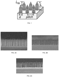
01 Fabrication methods for silicon micropillars
Various techniques are employed to create silicon micropillars, including photolithography, etching processes, and deposition methods. These fabrication methods allow for precise control over the size, shape, and spacing of the micropillars, which is crucial for achieving desired surface textures and properties.- Fabrication methods for silicon micropillars: Various techniques are employed to create silicon micropillars, including photolithography, etching processes, and deposition methods. These fabrication methods allow for precise control over the size, shape, and spacing of the micropillars, which is crucial for achieving desired surface textures and properties.
- Applications of silicon micropillar surfaces: Silicon micropillar surfaces find applications in diverse fields such as microelectronics, photovoltaics, and biomedical devices. The unique surface texture provided by these micropillars can enhance device performance, improve light trapping in solar cells, and modify surface wettability for specific applications.
- Optical properties of silicon micropillar surfaces: The surface texture created by silicon micropillars significantly influences the optical properties of the material. These structures can reduce reflectance, enhance light absorption, and create unique color effects through light interference. The ability to control these optical properties makes silicon micropillar surfaces valuable for various optoelectronic applications.
- Wettability control using silicon micropillars: Silicon micropillar surface textures can be designed to control the wettability of the surface, ranging from superhydrophobic to superhydrophilic. This control is achieved by manipulating the size, spacing, and geometry of the micropillars, as well as applying additional surface treatments. The ability to tune wettability is valuable for self-cleaning surfaces, microfluidics, and anti-fouling applications.
- Integration of silicon micropillars in sensor technologies: Silicon micropillar surface textures are being integrated into various sensor technologies to enhance sensitivity and specificity. The increased surface area and unique properties of these structures make them suitable for chemical and biological sensing applications. Additionally, the micropillars can be functionalized or combined with other materials to create advanced sensing platforms.
02 Applications of silicon micropillar surfaces
Silicon micropillar surfaces find applications in diverse fields such as microelectronics, photovoltaics, and biomedical devices. The unique surface texture provided by these micropillars can enhance device performance, improve light trapping in solar cells, and modify surface wettability for specific applications.Expand Specific Solutions03 Optical properties of silicon micropillar surfaces
The surface texture created by silicon micropillars can significantly influence the optical properties of the material. These structures can reduce reflectance, enhance light absorption, and create unique color effects through light interference. The ability to control these optical properties makes silicon micropillar surfaces valuable for various optoelectronic applications.Expand Specific Solutions04 Wettability control using silicon micropillars
Silicon micropillar surface textures can be designed to control the wettability of the surface, ranging from superhydrophobic to superhydrophilic. By adjusting the dimensions and arrangement of the micropillars, it is possible to create surfaces with specific water contact angles and adhesion properties, which is useful for self-cleaning surfaces and microfluidic devices.Expand Specific Solutions05 Integration of silicon micropillars in sensor technologies
Silicon micropillar surface textures are being integrated into various sensor technologies to enhance sensitivity and specificity. The increased surface area and unique properties of these structures make them suitable for chemical and biological sensing applications, as well as for improving the performance of pressure and touch sensors.Expand Specific Solutions
Key Players in Nanotechnology Industry
The silicon micropillars in nanotextured surfaces market is in its growth stage, with increasing research and commercial applications. The market size is expanding due to rising demand in sectors like electronics, energy, and biomedical. Technologically, it's progressing from lab-scale to industrial implementation. Companies like Corning, HP, and Canon are advancing the field through R&D and product development. Academic institutions such as MIT, Zhejiang University, and EPFL are contributing fundamental research. The technology's maturity varies across applications, with some areas nearing commercialization while others remain in early research stages. Collaboration between industry and academia is driving innovation and accelerating market growth.
Corning, Inc.
Technical Solution: Corning has developed innovative approaches to creating silicon micropillar arrays for nanotextured surfaces, focusing on large-scale manufacturing processes. Their technique involves a combination of nanoimprint lithography and reactive ion etching to create uniform micropillar arrays over large areas. Corning's silicon micropillars typically range from 0.5-5 μm in height and 100-500 nm in diameter[1]. These structures have been primarily applied to enhance the optical properties of glass substrates, creating anti-reflective and self-cleaning surfaces. Corning has demonstrated a reduction in surface reflectance by up to 99.5% across a broad spectrum of wavelengths[2]. Additionally, they have explored the use of these micropillar arrays in improving the efficiency of thin-film solar cells, showing an increase in light absorption by up to 30%[3]. Corning has also investigated the durability of these structures, developing coatings that can protect the micropillars while maintaining their functional properties.
Strengths: Large-scale manufacturing capability suitable for industrial applications. Focus on durability and integration with existing glass products. Weaknesses: Limited flexibility in micropillar geometries compared to some academic research approaches. Primarily focused on optical applications rather than a broader range of functionalities.
The Regents of the University of California
Technical Solution: The University of California has made significant contributions to the field of silicon micropillars in nanotextured surfaces. Their research focuses on developing multifunctional surfaces using precisely controlled silicon micropillar arrays. Using a combination of e-beam lithography and deep reactive ion etching (DRIE), they have created micropillars with heights ranging from 1-50 μm and diameters from 50-500 nm[1]. These structures have been applied to create superhydrophobic surfaces with water contact angles exceeding 160° and extremely low contact angle hysteresis[2]. The team has also explored the use of these micropillars in enhancing the efficiency of thin-film solar cells, demonstrating up to a 40% increase in light absorption[3]. Additionally, they have investigated the use of silicon micropillars in biosensing applications, showing enhanced sensitivity for protein detection due to increased surface area and unique optical properties[4].
Strengths: High precision in micropillar fabrication allows for tailored surface properties. Diverse applications ranging from water repellency to biosensing. Weaknesses: High-cost fabrication methods may limit large-scale production. Potential fragility of very high aspect ratio structures.
Innovative Micropillar Designs and Patents
Surface nanoreplication using polymer nanomasks
PatentActiveEP2948816A1
Innovation
- The method involves depositing a block copolymer and homopolymer mixture as a thin film on a substrate, forming nanoholes, and using a self-assembled polymer nanomask to replicate nanopillared surfaces, allowing for scalable, low-cost nano-texturing at room temperature.
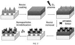
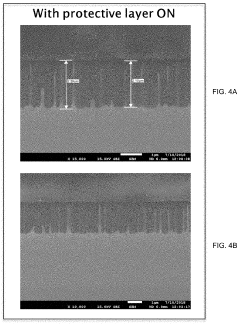
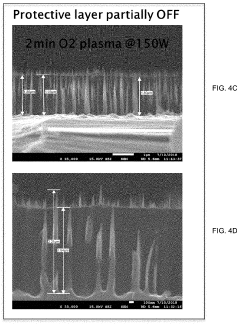
Localized functionalization of nanotextured surfaces
PatentActiveUS20200039819A1
Innovation
- A method involving the deposition of a protective coating on nanotextured materials, selective removal of the coating to expose specific portions, modification of these exposed areas with functional groups, and subsequent removal of the coating, allowing for precise and scalable functionalization of nanotextured surfaces.
Environmental Impact of Nanotexturing
The environmental impact of nanotexturing, particularly in the context of silicon micropillars, is a critical consideration in the development and application of this technology. Nanotextured surfaces, while offering numerous benefits in various fields, also present potential environmental challenges that must be carefully evaluated and addressed.
One of the primary environmental concerns associated with nanotexturing is the potential release of nanoparticles into the environment during the manufacturing process or throughout the lifecycle of nanotextured products. These nanoparticles, if not properly contained or managed, could potentially enter ecosystems and pose risks to wildlife and human health. The small size of these particles makes them highly mobile in air and water, potentially leading to widespread distribution in the environment.
The production of nanotextured surfaces, especially those involving silicon micropillars, often requires the use of specialized chemicals and processes. These may include etching agents, cleaning solvents, and other materials that could have adverse environmental effects if not properly handled or disposed of. The energy-intensive nature of some nanotexturing processes also contributes to their environmental footprint, particularly in terms of greenhouse gas emissions and resource consumption.
However, it is important to note that nanotextured surfaces, including those created with silicon micropillars, can also offer significant environmental benefits. For instance, these surfaces can enhance the efficiency of solar cells, leading to increased renewable energy production and reduced reliance on fossil fuels. Similarly, nanotextured surfaces can improve the performance of water filtration systems, potentially addressing water scarcity issues in many parts of the world.
The durability and longevity of nanotextured surfaces can also contribute to sustainability efforts by reducing the need for frequent replacements and minimizing waste generation. Additionally, some nanotextured surfaces exhibit self-cleaning properties, which can reduce the use of chemical cleaning agents and water, further lessening environmental impact.
As research in this field progresses, there is a growing focus on developing more environmentally friendly nanotexturing processes. This includes exploring alternative materials and methods that minimize the use of harmful chemicals and reduce energy consumption. Efforts are also being made to improve the recyclability and end-of-life management of nanotextured products to ensure a more circular and sustainable approach to their use.
In conclusion, while nanotexturing, including the use of silicon micropillars, presents some environmental challenges, it also offers significant potential for positive environmental impact. The key lies in balancing these factors through responsible development, application, and management of this technology. Ongoing research and innovation in this field are crucial for maximizing the benefits of nanotextured surfaces while minimizing their environmental footprint.
Scalability and Cost Analysis
The scalability and cost analysis of silicon micropillars in nanotextured surfaces is a critical consideration for their widespread adoption in industrial applications. As the demand for advanced surface engineering solutions grows, the ability to produce these structures at scale becomes increasingly important.
From a manufacturing perspective, silicon micropillars can be fabricated using various techniques, including photolithography, etching, and deposition processes. The scalability of these methods varies significantly. Photolithography, while precise, may face challenges in large-scale production due to its time-consuming nature and equipment costs. Etching techniques, such as reactive ion etching (RIE) or deep reactive ion etching (DRIE), offer better scalability potential but require careful process control to maintain uniformity across large surface areas.
Cost considerations for silicon micropillar production encompass several factors. The primary cost drivers include raw materials, particularly high-purity silicon wafers, specialized equipment for fabrication processes, and operational expenses such as clean room maintenance and skilled labor. As production scales up, economies of scale can potentially reduce per-unit costs, but this is contingent on optimizing manufacturing processes and minimizing material waste.
The integration of silicon micropillars into existing manufacturing lines presents both opportunities and challenges. While it offers the potential for enhanced product performance, it may require significant initial investment in equipment and process development. Companies must carefully evaluate the return on investment, considering factors such as improved product functionality, market demand, and competitive advantage.
Environmental and sustainability aspects also play a role in scalability and cost analysis. The energy-intensive nature of some fabrication processes may lead to higher operational costs and environmental concerns. However, advancements in green manufacturing techniques and the potential for silicon micropillars to contribute to more efficient products (e.g., improved solar cells or self-cleaning surfaces) could offset these considerations in the long term.
As the technology matures, research into alternative materials and fabrication methods may further improve scalability and reduce costs. For instance, exploring the use of polymer-based micropillars or developing roll-to-roll fabrication techniques could potentially offer more cost-effective solutions for large-scale production.
In conclusion, while silicon micropillars show promising potential for nanotextured surfaces, their widespread adoption hinges on overcoming scalability challenges and optimizing production costs. Continued research and development efforts, coupled with strategic investments in manufacturing capabilities, will be crucial in realizing the full potential of this technology across various industries.
Unlock deeper insights with Patsnap Eureka Quick Research — get a full tech report to explore trends and direct your research. Try now!
Generate Your Research Report Instantly with AI Agent
Supercharge your innovation with Patsnap Eureka AI Agent Platform!