Silicon Micropillars and Their Impact on Semiconductor Industries
JUL 9, 202510 MIN READ
Generate Your Research Report Instantly with AI Agent
Patsnap Eureka helps you evaluate technical feasibility & market potential.
Silicon Micropillars Evolution and Objectives
Silicon micropillars have emerged as a groundbreaking technology in the semiconductor industry, revolutionizing the way we approach chip design and manufacturing. The evolution of this technology can be traced back to the early 2000s when researchers began exploring ways to enhance the performance and efficiency of semiconductor devices. The primary objective of silicon micropillars is to overcome the limitations of traditional planar semiconductor structures by leveraging three-dimensional architectures.
The development of silicon micropillars has been driven by the need to address several key challenges in the semiconductor industry. These include the demand for higher transistor density, improved power efficiency, and enhanced heat dissipation. As Moore's Law continues to push the boundaries of semiconductor technology, silicon micropillars offer a promising solution to extend the scaling of integrated circuits beyond conventional limits.
One of the main goals of silicon micropillar research is to achieve vertical integration of transistors, allowing for a significant increase in device density without compromising performance. This vertical architecture enables the creation of 3D integrated circuits, which can potentially lead to smaller chip sizes, reduced power consumption, and improved overall system performance.
Another critical objective is to enhance the electrical properties of semiconductor devices. Silicon micropillars provide a larger surface area for charge carriers to flow, potentially leading to higher current densities and faster switching speeds. This improvement in electrical characteristics is particularly valuable for applications in high-performance computing and advanced mobile devices.
The evolution of silicon micropillars has also been closely tied to advancements in fabrication techniques. Researchers have developed various methods for creating these structures, including deep reactive ion etching, selective epitaxial growth, and template-assisted approaches. Each of these techniques has its own set of advantages and challenges, contributing to the ongoing refinement of silicon micropillar technology.
As the technology continues to mature, the semiconductor industry is exploring new applications and integration strategies for silicon micropillars. These include their use in next-generation memory devices, advanced sensors, and photonic integrated circuits. The versatility of silicon micropillars opens up possibilities for creating multifunctional devices that combine different functionalities on a single chip.
Looking ahead, the objectives for silicon micropillar technology include further miniaturization, improved reliability, and cost-effective manufacturing processes. Researchers are also investigating ways to combine silicon micropillars with other emerging technologies, such as 2D materials and quantum computing, to create hybrid systems with enhanced capabilities.
Market Demand Analysis for Advanced Semiconductors
The semiconductor industry has been experiencing a surge in demand for advanced semiconductors, driven by the rapid evolution of technologies such as artificial intelligence, 5G networks, Internet of Things (IoT), and autonomous vehicles. This market demand analysis focuses on the impact of silicon micropillars on the semiconductor industry and their potential to meet the growing need for more powerful and efficient chips.
The global semiconductor market is projected to reach unprecedented heights in the coming years, with a significant portion attributed to advanced semiconductors. The demand for high-performance computing, data centers, and edge computing solutions has created a strong market pull for innovative semiconductor technologies. Silicon micropillars, with their potential to enhance chip performance and reduce power consumption, are positioned to address these market needs effectively.
In the consumer electronics sector, the demand for smaller, faster, and more energy-efficient devices continues to grow. Smartphones, tablets, and wearable technologies require advanced semiconductors that can deliver superior performance while maintaining battery life. Silicon micropillars offer a promising solution to these challenges, potentially enabling the next generation of mobile devices with improved capabilities and longer battery life.
The automotive industry is another key driver of demand for advanced semiconductors. As vehicles become increasingly electrified and autonomous, the need for sophisticated chips that can handle complex computations while operating in harsh environments has skyrocketed. Silicon micropillars could play a crucial role in developing semiconductors that meet the stringent requirements of the automotive sector, including high reliability, thermal management, and resistance to electromagnetic interference.
In the industrial sector, the adoption of Industry 4.0 technologies and smart manufacturing processes is creating a robust demand for advanced semiconductors. Silicon micropillars could enable the development of sensors and control systems with enhanced sensitivity and efficiency, crucial for the implementation of IoT and machine-to-machine communication in industrial settings.
The data center and cloud computing markets are experiencing exponential growth, driving demand for high-performance processors and memory chips. Silicon micropillars have the potential to address the increasing need for faster data processing and reduced energy consumption in these applications, making them a technology of significant interest to major cloud service providers and data center operators.
As governments and private entities invest heavily in artificial intelligence and machine learning technologies, the demand for specialized AI chips is soaring. Silicon micropillars could contribute to the development of more efficient AI processors, capable of handling complex neural networks and machine learning algorithms with improved speed and energy efficiency.
The ongoing global rollout of 5G networks and the anticipated transition to 6G in the future are creating substantial demand for advanced semiconductors in the telecommunications sector. Silicon micropillars may offer solutions for developing high-frequency, low-latency chips essential for next-generation wireless communication technologies.
In conclusion, the market demand for advanced semiconductors is robust and diverse, spanning multiple industries and applications. Silicon micropillars represent a promising technology that could address many of the current and future needs in the semiconductor industry, potentially revolutionizing chip design and performance across various sectors.
Current State and Challenges in Micropillar Technology
Silicon micropillar technology has made significant strides in recent years, revolutionizing various aspects of semiconductor industries. The current state of this technology is characterized by advanced fabrication techniques and a wide range of applications across multiple sectors. Micropillars, typically ranging from a few nanometers to several micrometers in diameter, are now being produced with unprecedented precision and uniformity.
One of the key advancements in micropillar technology is the development of high-aspect-ratio structures, which allow for increased surface area and improved performance in various applications. These structures have found particular success in photovoltaic cells, where they enhance light trapping and increase overall efficiency. Additionally, micropillars have shown promise in the field of microfluidics, enabling the creation of more sensitive and accurate biosensors.
Despite these achievements, the technology faces several challenges that hinder its widespread adoption and further development. One of the primary obstacles is the scalability of production processes. While researchers have demonstrated impressive results in laboratory settings, translating these techniques to large-scale manufacturing remains a significant hurdle. The complexity and cost of equipment required for precise micropillar fabrication pose challenges for mass production and commercialization.
Another critical challenge lies in the control of micropillar properties at the nanoscale. As dimensions shrink, the influence of surface effects becomes more pronounced, leading to variations in electrical and mechanical properties. Achieving consistent performance across large arrays of micropillars requires overcoming these nanoscale variations, which demands advanced characterization techniques and process control methods.
The integration of micropillar structures with existing semiconductor technologies also presents challenges. Compatibility issues arise when incorporating these structures into conventional device architectures, necessitating the development of new design paradigms and fabrication processes. This integration challenge is particularly evident in the field of microelectronics, where the incorporation of micropillars into transistor designs holds promise for improved performance but requires significant modifications to established manufacturing techniques.
Material selection and optimization remain ongoing challenges in micropillar technology. While silicon remains the dominant material due to its well-established processing techniques, researchers are exploring alternative materials such as III-V semiconductors and various composites to enhance specific properties. However, each new material introduces its own set of fabrication and integration challenges, requiring extensive research and development efforts.
As the technology continues to evolve, addressing these challenges will be crucial for realizing the full potential of silicon micropillars in semiconductor industries. Collaborative efforts between academia and industry, coupled with advancements in nanofabrication techniques and materials science, will be key to overcoming these obstacles and driving further innovation in this promising field.
Existing Micropillar Fabrication Techniques
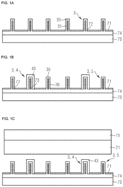
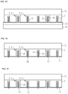
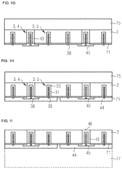
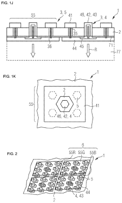
01 Fabrication methods for silicon micropillars
Various techniques are employed to create silicon micropillars, including etching processes, lithography, and deposition methods. These fabrication methods allow for precise control over the size, shape, and arrangement of the micropillars, which is crucial for their performance in different applications.- Fabrication of silicon micropillars: Silicon micropillars are fabricated using various techniques such as etching, lithography, and deposition processes. These structures can be created with precise dimensions and patterns, offering applications in microelectronics, sensors, and energy devices.
- Applications in solar cells and photovoltaics: Silicon micropillars are utilized in solar cell and photovoltaic technologies to enhance light absorption and improve overall efficiency. The unique structure of micropillars allows for better light trapping and increased surface area for energy conversion.
- Use in microfluidic devices and lab-on-a-chip systems: Silicon micropillars are incorporated into microfluidic devices and lab-on-a-chip systems for various applications, including particle separation, fluid mixing, and biosensing. The micropillar arrays can be designed to control fluid flow and enhance analytical performance.
- Integration with MEMS and NEMS devices: Silicon micropillars are integrated into Micro-Electro-Mechanical Systems (MEMS) and Nano-Electro-Mechanical Systems (NEMS) devices. These structures can be used for sensing, actuation, and energy harvesting in miniaturized systems.
- Surface functionalization and modification: The surface of silicon micropillars can be functionalized or modified to enhance their properties for specific applications. This includes coating with various materials, chemical treatments, or creating hybrid structures to improve performance in areas such as sensing, catalysis, or biomedical applications.
02 Applications in solar cells and photovoltaics
Silicon micropillars are utilized in solar cell and photovoltaic technologies to enhance light absorption and improve overall efficiency. The unique structure of micropillars allows for better light trapping and increased surface area, leading to improved energy conversion rates.Expand Specific Solutions03 Use in microfluidic devices and sensors
Silicon micropillars are incorporated into microfluidic devices and sensors for various applications, including chemical analysis, biological detection, and environmental monitoring. The micropillars can be functionalized or modified to enhance sensitivity and specificity in sensing applications.Expand Specific Solutions04 Integration with MEMS and NEMS technologies
Silicon micropillars are integrated with Micro-Electro-Mechanical Systems (MEMS) and Nano-Electro-Mechanical Systems (NEMS) to create advanced devices with enhanced functionalities. This integration allows for the development of miniaturized sensors, actuators, and other micro/nano-scale devices with improved performance characteristics.Expand Specific Solutions05 Surface modification and functionalization
Various techniques are employed to modify and functionalize the surface of silicon micropillars, enhancing their properties for specific applications. These modifications can include chemical treatments, coatings, or the addition of functional groups to tailor the micropillars for use in areas such as catalysis, drug delivery, or advanced materials.Expand Specific Solutions
Key Players in Semiconductor Micropillar Research
The research on silicon micropillars and their impact on semiconductor industries is currently in a growth phase, with increasing market potential and technological advancements. The global semiconductor industry, valued at over $500 billion, is driving demand for innovative solutions like silicon micropillars. Major players such as Taiwan Semiconductor Manufacturing Co., Ltd., Samsung Electronics, and Intel are investing heavily in this technology. Companies like NXP Semiconductors and Infineon Technologies are also exploring applications in power electronics and sensors. Academic institutions, including Nanjing University and Yale University, are contributing to fundamental research, while national laboratories like Forschungszentrum Jülich GmbH are advancing the technology's practical applications. The collaboration between industry leaders and research institutions is accelerating the maturation of silicon micropillar technology, positioning it as a potential game-changer in semiconductor manufacturing.
Taiwan Semiconductor Manufacturing Co., Ltd.
Technical Solution: TSMC has been investing in silicon micropillar research to maintain its leadership in advanced semiconductor manufacturing. Their approach focuses on integrating silicon micropillars into logic and memory devices to achieve higher performance and lower power consumption. TSMC's research involves developing novel fabrication techniques for creating high-aspect-ratio silicon micropillars with precise control over dimensions and doping profiles[7]. The company has demonstrated the ability to produce silicon micropillars with diameters as small as 5 nm and heights exceeding 50 nm, achieving aspect ratios greater than 10:1[8]. TSMC's silicon micropillar technology also incorporates advanced strain engineering and gate-all-around architectures to enhance carrier mobility and electrostatic control[9].
Strengths: Advanced fabrication techniques, high-precision control, integration with logic and memory devices. Weaknesses: Increased process complexity, potential yield challenges at extreme dimensions.
Infineon Technologies AG
Technical Solution: Infineon has been exploring silicon micropillar technology for power semiconductor applications. Their research focuses on developing vertical power devices using silicon micropillars to achieve higher breakdown voltages and lower on-resistance. Infineon's approach involves creating arrays of silicon micropillars with optimized doping profiles and termination structures to enhance electric field distribution and current handling capabilities[10]. The company has demonstrated the ability to fabricate silicon micropillars with diameters ranging from 1 to 10 μm and heights exceeding 100 μm, achieving aspect ratios greater than 10:1[11]. Infineon's silicon micropillar technology also incorporates advanced passivation and metallization techniques to improve device reliability and thermal performance[12].
Strengths: Expertise in power semiconductor applications, high-voltage device optimization, advanced passivation techniques. Weaknesses: Potential challenges in scaling to smaller dimensions, increased manufacturing costs.
Core Innovations in Silicon Micropillar Design
Optoelectronic Semiconductor Component and Method for Producing Optoelectronic Semiconductor Components
PatentActiveUS20210005660A1
Innovation
- The development of an optoelectronic semiconductor component comprising semiconductor pillars with distinct emitter and contact pillars, where the contact pillars extend through an electrical isolation layer and are coated with an ohmic conductive outer layer, allowing for uniform energization and precise electrical contacting of sub-micron structures.
Micro-pillar assisted semiconductor bonding
PatentActiveUS20150364441A1
Innovation
- The use of micro pillars on the silicon substrate to penetrate and break indium oxide, reducing the initial surface contact area and heat transfer, allowing for easier melting of indium and improved bonding by modulating heat and pressure transfer.
Environmental Impact of Micropillar Production
The production of silicon micropillars, while crucial for advancing semiconductor technologies, carries significant environmental implications that warrant careful consideration. The manufacturing process involves several stages that can potentially impact the environment, including raw material extraction, energy-intensive fabrication, and waste management.
The primary environmental concern in micropillar production is the extensive use of silicon, which requires mining and processing of silica sand. This extraction process can lead to habitat destruction, soil erosion, and water pollution in mining areas. Furthermore, the purification of silicon to the high grades required for semiconductor applications is an energy-intensive process, contributing to increased carbon emissions and resource depletion.
During the fabrication of micropillars, various chemicals and gases are utilized, including hydrofluoric acid, sulfuric acid, and hydrogen peroxide. The handling and disposal of these substances pose potential risks to air and water quality if not managed properly. Additionally, the etching processes used to create micropillars generate hazardous waste that requires specialized treatment and disposal methods to prevent environmental contamination.
Water consumption is another critical environmental factor in micropillar production. The semiconductor industry is known for its high water usage, particularly in cleaning and cooling processes. The production of micropillars may exacerbate this issue, potentially straining local water resources in areas where manufacturing facilities are located.
Energy consumption in micropillar production is substantial, primarily due to the need for cleanroom environments, precise temperature control, and the operation of sophisticated manufacturing equipment. This high energy demand often translates to increased greenhouse gas emissions, depending on the energy sources used by production facilities.
On a positive note, the development of silicon micropillars may contribute to more efficient semiconductor devices, potentially leading to reduced energy consumption in end-use applications. This could offset some of the environmental impacts associated with their production over the long term. Additionally, ongoing research into more sustainable manufacturing processes and materials may help mitigate some of the environmental challenges associated with micropillar production.
As the semiconductor industry continues to advance, it is crucial to balance technological progress with environmental stewardship. This necessitates ongoing efforts to optimize production processes, reduce waste, and explore more sustainable alternatives in micropillar manufacturing. Collaboration between industry stakeholders, researchers, and environmental experts will be essential in developing strategies to minimize the environmental footprint of silicon micropillar production while maximizing its technological benefits.
Intellectual Property Landscape in Micropillar Technology
The intellectual property landscape in micropillar technology is characterized by a complex network of patents and proprietary innovations. Major semiconductor companies and research institutions have been actively filing patents related to silicon micropillars, reflecting the growing importance of this technology in the industry. The patent landscape is primarily dominated by key players such as Intel, Samsung, TSMC, and IBM, who have been investing heavily in research and development of micropillar structures for advanced semiconductor applications.
Patent filings in this domain cover a wide range of aspects, including fabrication methods, structural designs, and integration techniques for micropillars in various semiconductor devices. A significant portion of the patents focuses on improving the electrical and thermal performance of micropillar-based interconnects, addressing challenges such as resistance reduction and heat dissipation in high-density chip designs.
Another prominent area of patent activity revolves around the use of micropillars in advanced packaging technologies, particularly in 3D integration and through-silicon via (TSV) applications. These patents often describe novel approaches to enhance signal integrity, reduce crosstalk, and improve overall system performance in multi-chip modules and system-in-package solutions.
Emerging trends in the patent landscape include the application of micropillars in next-generation memory technologies, such as 3D NAND and emerging non-volatile memory architectures. Patents in this area typically focus on innovative ways to increase memory density, improve data transfer rates, and enhance overall reliability using micropillar structures.
The geographical distribution of patents shows a concentration in regions with strong semiconductor industries, particularly in the United States, South Korea, Taiwan, and Japan. However, there is a noticeable increase in patent filings from China in recent years, indicating the country's growing emphasis on semiconductor technology development.
Collaborative research efforts between academic institutions and industry players have also resulted in joint patent filings, highlighting the importance of partnerships in advancing micropillar technology. These collaborations often focus on fundamental research and novel applications of micropillars in emerging fields such as quantum computing and neuromorphic systems.
As the semiconductor industry continues to push the boundaries of miniaturization and performance, the intellectual property landscape in micropillar technology is expected to become increasingly competitive. Companies are likely to focus on building strong patent portfolios to protect their innovations and secure their market positions in this critical area of semiconductor technology.
Unlock deeper insights with Patsnap Eureka Quick Research — get a full tech report to explore trends and direct your research. Try now!
Generate Your Research Report Instantly with AI Agent
Supercharge your innovation with Patsnap Eureka AI Agent Platform!