

Best Practices for Chiplet Assembly and Testing
JUL 16, 20259 MIN READ
Generate Your Research Report Instantly with AI Agent
Patsnap Eureka helps you evaluate technical feasibility & market potential.
Chiplet Tech Evolution
The evolution of chiplet technology represents a significant paradigm shift in semiconductor design and manufacturing. This approach, which involves breaking down complex system-on-chip (SoC) designs into smaller, modular components called chiplets, has gained momentum over the past decade as a response to the challenges posed by Moore's Law and the increasing demand for specialized, high-performance computing solutions.
The concept of chiplets emerged in the early 2010s as semiconductor companies sought ways to overcome the limitations of traditional monolithic chip designs. The initial focus was on developing standardized interfaces and protocols to enable communication between different chiplets. This led to the creation of various interconnect technologies, such as Intel's Embedded Multi-die Interconnect Bridge (EMIB) and AMD's Infinity Fabric.
As the technology matured, the industry witnessed a rapid progression in chiplet design and integration techniques. By the mid-2010s, companies began to demonstrate the feasibility of chiplet-based architectures in commercial products. AMD's Zen-based processors, introduced in 2017, marked a significant milestone in chiplet adoption, showcasing the potential for improved performance and cost-effectiveness.
The latter half of the 2010s saw an acceleration in chiplet innovation, with a focus on enhancing integration density, reducing power consumption, and improving overall system performance. Advanced packaging technologies, such as TSMC's Integrated Fan-Out (InFO) and Intel's Foveros, played a crucial role in enabling more sophisticated chiplet designs.
As we entered the 2020s, the chiplet ecosystem expanded rapidly, with increased collaboration between semiconductor companies, foundries, and packaging specialists. This period witnessed the emergence of industry standards and consortia, such as the Universal Chiplet Interconnect Express (UCIe), aimed at promoting interoperability and accelerating chiplet adoption across the industry.
The most recent developments in chiplet technology have focused on addressing the challenges of heterogeneous integration, enabling the combination of chiplets manufactured using different process nodes and even different materials. This has opened up new possibilities for creating highly customized, application-specific solutions that can meet the diverse needs of emerging technologies such as artificial intelligence, 5G, and edge computing.
Looking ahead, the chiplet technology roadmap is poised for further advancements in areas such as 3D integration, optical interconnects, and advanced materials. These innovations are expected to drive continued improvements in performance, energy efficiency, and cost-effectiveness, solidifying the role of chiplets as a cornerstone of future semiconductor design and manufacturing strategies.
Market Demand Analysis
The market demand for chiplet assembly and testing solutions is experiencing significant growth, driven by the increasing complexity and performance requirements of modern semiconductor devices. As traditional monolithic chip designs reach their physical limits, chiplet-based architectures have emerged as a promising alternative, offering improved scalability, flexibility, and cost-effectiveness.
The global semiconductor industry is witnessing a shift towards chiplet technology, with major players like Intel, AMD, and TSMC investing heavily in this approach. This trend is fueled by the need for more powerful and efficient computing solutions across various sectors, including data centers, artificial intelligence, 5G networks, and high-performance computing.
The demand for chiplet assembly and testing solutions is particularly strong in the data center and cloud computing markets. These sectors require high-performance, energy-efficient processors that can handle massive workloads. Chiplet-based designs allow for the integration of specialized components, optimizing performance and power consumption for specific applications.
In the consumer electronics market, chiplet technology is gaining traction in smartphones, tablets, and other mobile devices. The ability to mix and match different chiplets enables manufacturers to create customized solutions that balance performance, power efficiency, and cost. This flexibility is crucial in a highly competitive market where product differentiation is key.
The automotive industry is another significant driver of demand for chiplet assembly and testing solutions. As vehicles become more connected and autonomous, the need for advanced semiconductor solutions increases. Chiplet-based designs offer the potential for more powerful and efficient automotive processors, capable of handling complex tasks such as real-time sensor data processing and decision-making.
The market for chiplet assembly and testing equipment and services is expected to grow substantially in the coming years. This growth is supported by the increasing adoption of chiplet technology across various industries and the need for specialized tools and processes to ensure reliable integration and testing of multi-chip modules.
However, the market also faces challenges, including the need for standardization in chiplet interfaces and packaging technologies. Overcoming these hurdles will be crucial for wider adoption and interoperability between different chiplet designs and manufacturers.
As the demand for more advanced and specialized semiconductor solutions continues to rise, the market for chiplet assembly and testing is poised for significant expansion. Companies that can offer innovative, reliable, and cost-effective solutions in this space are likely to see substantial growth opportunities in the coming years.
Assembly Challenges
Chiplet assembly presents several significant challenges that must be addressed to ensure optimal performance and reliability. One of the primary hurdles is achieving precise alignment and bonding between multiple chiplets and the interposer or substrate. The miniaturization of components and the increasing complexity of interconnects demand extremely tight tolerances, often in the range of micrometers or even nanometers. This level of precision requires advanced pick-and-place equipment and sophisticated alignment techniques.
Thermal management is another critical challenge in chiplet assembly. As multiple high-performance chiplets are integrated into a single package, heat dissipation becomes a major concern. The compact nature of chiplet designs can lead to localized hotspots and thermal gradients, which may impact performance and reliability. Innovative cooling solutions, such as integrated liquid cooling or advanced thermal interface materials, are being explored to address these thermal challenges.
The heterogeneous integration of chiplets also introduces complexities in terms of material compatibility and stress management. Different chiplets may have varying coefficients of thermal expansion, which can lead to warpage and mechanical stress during thermal cycling. This stress can potentially cause delamination, cracking, or failure of interconnects. Careful material selection and stress mitigation strategies are essential to ensure long-term reliability of chiplet-based systems.
Another significant challenge lies in the realm of testing and quality assurance. Traditional testing methods designed for monolithic chips may not be sufficient for chiplet-based designs. Each chiplet needs to be tested individually before assembly, and the entire system requires comprehensive testing after integration. This multi-stage testing process increases complexity and potentially impacts yield and cost. Developing efficient and effective testing methodologies for chiplet assemblies is an ongoing area of research and development.
Signal integrity and power delivery also present unique challenges in chiplet assembly. The high-speed interconnects between chiplets and the substrate must maintain signal quality while minimizing crosstalk and electromagnetic interference. Power delivery networks need to be carefully designed to ensure stable and efficient power distribution across all chiplets. These challenges become more pronounced as data rates increase and power requirements become more demanding.
Lastly, the assembly process itself requires careful consideration of contamination control and yield management. The increased number of assembly steps and handling of multiple components increases the risk of particle contamination, which can lead to defects and yield loss. Advanced clean room technologies and handling procedures are necessary to mitigate these risks and maintain high assembly yields.
Current Assembly Methods
01 Chiplet interconnection and integration
This approach focuses on developing advanced interconnection technologies for chiplets, including through-silicon vias (TSVs), micro-bumps, and interposers. These technologies enable high-bandwidth, low-latency communication between chiplets, facilitating the integration of multiple chiplets into a single package. The process involves precise alignment and bonding techniques to ensure reliable connections between chiplets and the substrate.- Chiplet interconnection and integration: This approach focuses on methods for interconnecting and integrating multiple chiplets into a single package. It involves advanced packaging technologies, such as 2.5D and 3D integration, to combine different chiplets with varying functionalities. The process may include the use of interposers, through-silicon vias (TSVs), and micro-bumps to establish connections between chiplets and facilitate high-bandwidth communication.
- Chiplet testing and verification: This category encompasses methods and systems for testing and verifying individual chiplets as well as the assembled multi-chiplet package. It includes pre-assembly testing of chiplets, in-situ testing during the assembly process, and post-assembly functional and performance verification. Advanced testing techniques may involve the use of built-in self-test (BIST) circuits, boundary scan testing, and high-speed I/O testing to ensure the reliability and functionality of the chiplet-based system.
- Thermal management in chiplet assemblies: This aspect addresses the challenges of heat dissipation in multi-chiplet packages. It involves innovative cooling solutions, such as integrated heat spreaders, microchannel cooling, and advanced thermal interface materials. The focus is on optimizing the thermal performance of chiplet assemblies to maintain reliability and prevent performance degradation due to overheating.
- Chiplet-to-chiplet communication protocols: This area focuses on developing and implementing efficient communication protocols between chiplets within a multi-chiplet package. It includes the design of high-speed interfaces, low-power interconnects, and standardized protocols to enable seamless data transfer between different chiplets. The goal is to optimize bandwidth, reduce latency, and improve overall system performance in chiplet-based architectures.
- Chiplet assembly process optimization: This category covers techniques for optimizing the chiplet assembly process to improve yield, reliability, and cost-effectiveness. It includes advanced pick-and-place technologies, precision alignment methods, and innovative bonding techniques such as hybrid bonding. The focus is on developing manufacturing processes that can handle the complexities of multi-chiplet integration while maintaining high throughput and quality.
02 Thermal management in chiplet assemblies
Effective thermal management is crucial in chiplet assemblies due to the high power density and heat generation. This involves designing innovative cooling solutions, such as integrated heat spreaders, microchannel cooling, and thermal interface materials. The goal is to efficiently dissipate heat from individual chiplets and maintain optimal operating temperatures across the entire assembly, ensuring reliability and performance.Expand Specific Solutions03 Testing methodologies for chiplet-based systems
Developing comprehensive testing strategies for chiplet-based systems is essential to ensure functionality and reliability. This includes pre-assembly testing of individual chiplets, in-situ testing during the assembly process, and post-assembly system-level testing. Advanced testing techniques may involve built-in self-test (BIST) circuits, boundary scan testing, and high-speed I/O testing to verify inter-chiplet communications and overall system performance.Expand Specific Solutions04 Packaging technologies for chiplet integration
Innovative packaging technologies are crucial for successful chiplet integration. This includes advanced substrate designs, 2.5D and 3D packaging techniques, and novel materials for improved electrical and thermal performance. The focus is on developing packaging solutions that can accommodate different chiplet sizes and types while providing high-density interconnects and maintaining signal integrity across the assembly.Expand Specific Solutions05 Yield improvement and defect management in chiplet assembly
Enhancing yield and managing defects in chiplet assembly processes is critical for cost-effective production. This involves developing strategies for known-good-die (KGD) selection, redundancy implementation, and defect isolation techniques. Advanced inspection and metrology tools are employed to identify and mitigate defects during the assembly process, improving overall yield and reliability of chiplet-based systems.Expand Specific Solutions
Key Industry Players
The chiplet assembly and testing market is in a growth phase, driven by increasing demand for advanced semiconductor solutions. The market size is expanding rapidly, with major players like Intel, GlobalFoundries, and Micron Technology investing heavily in this technology. The competitive landscape is characterized by a mix of established semiconductor giants and specialized foundries. Technologically, chiplet assembly is maturing, with companies like AMD and TSMC leading in implementation. However, standardization and integration challenges remain, indicating room for further innovation and market development. The involvement of research institutions such as the Indian Institute of Science suggests ongoing efforts to advance chiplet technologies and testing methodologies.
Intel Corp.
Technical Solution: Intel's approach to chiplet assembly and testing involves their advanced packaging technologies, particularly their Embedded Multi-die Interconnect Bridge (EMIB) and Foveros 3D packaging. For EMIB, Intel uses a small silicon bridge embedded in the package substrate to connect multiple chiplets, allowing high-bandwidth connections between dies[1]. This enables the integration of heterogeneous chiplets manufactured using different process nodes. For testing, Intel employs a hierarchical testing strategy, starting with individual chiplet testing, followed by interconnect testing, and finally full system-level testing. They have also developed specialized test structures and methodologies to ensure the reliability of the inter-chiplet connections[2].
Strengths: High-bandwidth connections, flexibility in integrating heterogeneous chiplets, and advanced 3D packaging capabilities. Weaknesses: Complexity in manufacturing and potential yield issues due to the intricate packaging process.
Texas Instruments Incorporated
Technical Solution: Texas Instruments focuses on chiplet assembly and testing for their analog and mixed-signal products. They employ their HyperFET technology, which allows for the integration of multiple chiplets in a single package, enabling higher performance and lower power consumption[7]. For testing, TI has developed a comprehensive Built-In Self-Test (BIST) strategy, which allows for in-situ testing of individual chiplets and interconnects. They also utilize adaptive test methodologies, where test parameters are dynamically adjusted based on real-time data to optimize test coverage and efficiency[8]. TI has invested in advanced probe technologies to enable high-speed, high-density testing of chiplets before assembly.
Strengths: Expertise in analog and mixed-signal integration, advanced BIST strategies, and adaptive testing methodologies. Weaknesses: Potential limitations in scaling to very large, high-performance digital chiplet designs.
Innovative Testing Tech
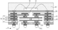
Semiconductor packaging structure and preparation method thereof
PatentActiveCN118431177B
Innovation
- A semiconductor packaging structure is designed, including a wiring structure with conductive lines, a dielectric layer, a chip and a cooling structure. The cooling structure is electrically connected to the conductive lines. After being energized, it vibrates to form an airflow pressure difference and communicates with the outside air through the first heat dissipation hole. An airflow pressure difference is formed to improve heat dissipation performance, and the chip is packaged through the dielectric layer and plastic sealing layer to avoid external power supply interference.
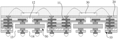
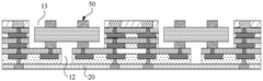
Chiplets 3D soic system integration and fabrication methods
PatentActiveUS20240088077A1
Innovation
- The formation of backside bridge structures on a first-tier chip allows for face-to-back bonding of second-tier chips, utilizing damascene structures to create short electrical paths that bypass the need for through-silicon vias, enabling efficient power and signal transfer between chips.


Supply Chain Impact
The adoption of chiplet technology in semiconductor manufacturing has significant implications for the supply chain, reshaping traditional production models and introducing new complexities. As chiplets enable the disaggregation of system-on-chip (SoC) designs into smaller, reusable components, the supply chain must adapt to accommodate this shift in production paradigms.
One of the primary impacts is the increased need for specialized suppliers and partners. Chiplet-based designs require expertise in various areas, including die-to-die interconnects, advanced packaging technologies, and system integration. This diversification of the supply chain creates opportunities for niche players to emerge and established companies to expand their offerings.
The modular nature of chiplets also introduces new challenges in inventory management and production planning. Manufacturers must coordinate the production and assembly of multiple chiplets from different sources, potentially increasing lead times and complicating logistics. This complexity necessitates more sophisticated supply chain management systems and closer collaboration between partners in the ecosystem.
Quality control and testing procedures are significantly impacted by chiplet technology. The need for known-good-die (KGD) becomes even more critical, as defects in individual chiplets can affect the entire system's performance. This places greater emphasis on robust testing methodologies throughout the supply chain, from individual chiplet manufacturers to system integrators.
The geographical distribution of the supply chain may also shift as a result of chiplet adoption. While some aspects of production may become more localized due to the ability to mix and match chiplets from different sources, the specialized nature of certain components may lead to concentration in specific regions with the necessary expertise and infrastructure.
Intellectual property (IP) management becomes more complex in a chiplet-based ecosystem. The modular nature of chiplets allows for greater reuse of IP, but it also requires clear agreements and protocols for sharing and protecting proprietary designs across the supply chain. This may lead to new business models and licensing arrangements among industry players.
In conclusion, the impact of chiplet technology on the semiconductor supply chain is multifaceted, requiring adaptations in partnerships, logistics, quality control, and IP management. As the industry continues to embrace this approach, supply chain strategies will need to evolve to support the flexibility and complexity inherent in chiplet-based designs.
Thermal Management
Thermal management is a critical aspect of chiplet assembly and testing, as it directly impacts the performance, reliability, and longevity of multi-chip modules. Effective thermal management strategies are essential to dissipate heat generated during operation and maintain optimal temperature levels across the chiplet array.
One of the primary challenges in chiplet thermal management is the increased power density resulting from the integration of multiple dies in a compact package. This concentration of heat-generating components necessitates advanced cooling solutions to prevent thermal hotspots and ensure uniform temperature distribution. Thermal interface materials (TIMs) play a crucial role in this context, facilitating efficient heat transfer between the chiplets and the heat spreader or cooling solution.
The selection of appropriate TIMs is a key consideration in chiplet assembly. High-performance thermal greases, phase-change materials, and metal-based TIMs are commonly employed to minimize thermal resistance at the interface. These materials must be carefully chosen based on their thermal conductivity, application method, and long-term stability to ensure optimal heat dissipation throughout the product lifecycle.
Advanced cooling techniques, such as liquid cooling and two-phase cooling systems, are increasingly being explored for high-performance chiplet designs. These solutions offer superior heat removal capabilities compared to traditional air cooling methods, enabling higher power densities and improved thermal management in complex multi-chip modules.
Thermal simulation and modeling tools are indispensable in the design and optimization of chiplet thermal management systems. Computational fluid dynamics (CFD) simulations and finite element analysis (FEA) allow engineers to predict temperature distributions, identify potential hotspots, and evaluate the effectiveness of various cooling strategies before physical prototyping.
During the testing phase, thermal characterization of chiplets is essential to validate thermal models and ensure compliance with temperature specifications. Infrared thermography and high-resolution thermal imaging techniques are employed to map temperature distributions across the chiplet array, providing valuable insights into thermal performance and potential areas for improvement.
The integration of on-chip temperature sensors and dynamic thermal management techniques enables real-time monitoring and adaptive control of chiplet temperatures during operation. This approach allows for intelligent power management and thermal throttling to maintain optimal performance while preventing thermal-induced failures.
As chiplet designs continue to evolve, emerging technologies such as embedded cooling channels and advanced packaging materials with enhanced thermal properties are being developed to address the growing thermal management challenges. These innovations promise to push the boundaries of chiplet performance and integration density while maintaining reliable thermal operation.
Unlock deeper insights with Patsnap Eureka Quick Research — get a full tech report to explore trends and direct your research. Try now!
Generate Your Research Report Instantly with AI Agent
Supercharge your innovation with Patsnap Eureka AI Agent Platform!