

Chiplet Advances Breaking Ground in Computational Methodologies
JUL 16, 20259 MIN READ
Generate Your Research Report Instantly with AI Agent
Patsnap Eureka helps you evaluate technical feasibility & market potential.
Chiplet Evolution and Objectives
Chiplet technology has emerged as a revolutionary approach in the semiconductor industry, transforming the landscape of computational methodologies. The evolution of chiplets can be traced back to the early 2010s when traditional monolithic chip designs began to face significant challenges in terms of scalability, performance, and cost-effectiveness.
The primary objective of chiplet technology is to overcome the limitations of monolithic chip designs by disaggregating complex systems-on-chip (SoCs) into smaller, more manageable components. This approach allows for greater flexibility in chip design, improved yield, and the ability to mix and match different process nodes within a single package.
As Moore's Law began to slow down, chiplets offered a promising alternative to continue advancing computational capabilities. The technology aims to provide a scalable solution for high-performance computing, enabling the integration of heterogeneous components and optimizing power efficiency.
The evolution of chiplets has been marked by several key milestones. Initially, the focus was on developing reliable interconnect technologies to enable seamless communication between different chiplets. This led to the development of advanced packaging technologies such as 2.5D and 3D integration.
Subsequently, industry standards emerged to facilitate interoperability between chiplets from different manufacturers. The Advanced Interface Bus (AIB) and Universal Chiplet Interconnect Express (UCIe) are examples of such standards that have played a crucial role in advancing chiplet technology.
Recent developments in chiplet technology have focused on enhancing performance and efficiency. This includes the exploration of novel materials for interconnects, advanced die-to-die bonding techniques, and the integration of artificial intelligence accelerators as specialized chiplets.
Looking ahead, the objectives of chiplet technology are multifaceted. One key goal is to further improve energy efficiency by optimizing the distribution of computational tasks across different chiplets. Another objective is to enhance the modularity and reusability of chip components, allowing for more rapid and cost-effective product development cycles.
Additionally, chiplet technology aims to enable more sophisticated heterogeneous computing architectures, combining different types of processors, memory, and specialized accelerators within a single package. This approach has the potential to revolutionize computational methodologies across various domains, from high-performance computing to edge devices in the Internet of Things (IoT) ecosystem.
Market Demand Analysis
The market demand for Chiplet technology is experiencing significant growth, driven by the increasing need for advanced computational methodologies across various industries. As traditional monolithic chip designs reach their physical and economic limits, Chiplet-based solutions are emerging as a viable alternative to meet the ever-growing demand for higher performance, lower power consumption, and cost-effective semiconductor solutions.
In the data center and cloud computing sector, the demand for Chiplet-based processors is particularly strong. These industries require high-performance, energy-efficient solutions to handle the exponential growth in data processing and storage needs. Chiplet technology allows for the integration of specialized processing units, memory, and I/O components, enabling customized solutions that can be tailored to specific workloads and applications.
The telecommunications industry, especially with the ongoing rollout of 5G networks and the anticipated 6G technology, is another key driver of Chiplet demand. The need for advanced radio frequency (RF) components and high-speed data processing capabilities in network infrastructure equipment is pushing manufacturers to adopt Chiplet-based designs for improved performance and energy efficiency.
In the automotive sector, the trend towards autonomous vehicles and advanced driver assistance systems (ADAS) is creating a substantial market for Chiplet technology. These applications require complex, high-performance computing solutions that can be efficiently packaged in limited spaces while meeting stringent reliability and safety standards.
The consumer electronics market is also showing increased interest in Chiplet-based solutions. As smartphones, tablets, and other personal devices continue to evolve, manufacturers are looking for ways to enhance performance and functionality while maintaining or reducing power consumption. Chiplet technology offers the flexibility to integrate diverse components, such as AI accelerators and specialized sensors, into compact form factors.
The industrial and manufacturing sectors are adopting Chiplet technology to support the growing trend of Industry 4.0 and smart manufacturing. These applications require powerful edge computing capabilities and real-time data processing, which can be efficiently addressed through Chiplet-based designs.
As the demand for artificial intelligence and machine learning continues to grow across various industries, Chiplet technology is well-positioned to meet the need for specialized, high-performance computing solutions. The ability to integrate different types of processing units, such as CPUs, GPUs, and AI accelerators, on a single package makes Chiplet-based designs particularly attractive for AI applications.
The market potential for Chiplet technology is further amplified by the ongoing global semiconductor shortage and the push for more resilient supply chains. Chiplet-based designs offer greater flexibility in sourcing and manufacturing, potentially alleviating some of the supply chain challenges faced by the industry.
Chiplet Technology Landscape
The chiplet technology landscape has undergone significant evolution in recent years, driven by the increasing demand for high-performance computing and the limitations of traditional monolithic chip designs. Chiplets represent a paradigm shift in semiconductor manufacturing, allowing for the disaggregation of complex systems-on-chip (SoCs) into smaller, more manageable components.
At the forefront of this landscape are advanced packaging technologies that enable the integration of multiple chiplets into a single package. These include 2.5D and 3D integration techniques, such as silicon interposers, through-silicon vias (TSVs), and advanced substrate technologies. These packaging innovations have paved the way for heterogeneous integration, allowing different chiplets manufactured using disparate process nodes to be combined efficiently.
The chiplet ecosystem is rapidly expanding, with major semiconductor companies and foundries investing heavily in this technology. Intel's Foveros and EMIB (Embedded Multi-die Interconnect Bridge) technologies, AMD's Infinity Fabric, and TSMC's CoWoS (Chip on Wafer on Substrate) are prime examples of industry-leading chiplet integration platforms. These technologies are enabling the creation of more powerful and efficient processors, GPUs, and AI accelerators.
Standardization efforts are also shaping the chiplet landscape. Initiatives like the Universal Chiplet Interconnect Express (UCIe) consortium are working towards establishing common interfaces and protocols for chiplet-to-chiplet communication. This standardization is crucial for fostering a more open and collaborative chiplet ecosystem, potentially leading to a marketplace where chiplets from different vendors can be mixed and matched.
The adoption of chiplet technology is expanding beyond traditional computing applications. It is finding its way into diverse fields such as 5G telecommunications, automotive electronics, and edge computing devices. This broad applicability is driving further innovation in chiplet design, manufacturing, and integration techniques.
However, challenges remain in the chiplet landscape. These include thermal management issues in densely packed multi-chiplet designs, the need for more sophisticated design and simulation tools, and the complexities of testing and validating multi-chiplet systems. Addressing these challenges is crucial for the continued advancement and widespread adoption of chiplet technology.
As the chiplet landscape continues to evolve, we can expect to see further innovations in interconnect technologies, packaging solutions, and design methodologies. The future may bring even more granular disaggregation of chip functionalities, potentially leading to highly customizable and efficient computing solutions tailored to specific application needs.
Current Chiplet Solutions
01 Chiplet interconnection and communication
This approach focuses on developing efficient methods for connecting and facilitating communication between multiple chiplets. It involves designing high-speed interfaces, optimizing data transfer protocols, and implementing advanced packaging technologies to enable seamless integration of chiplets in a single system.- Chiplet interconnection and communication: This approach focuses on developing efficient methods for connecting and facilitating communication between different chiplets in a multi-chip system. It involves designing high-speed interfaces, optimizing data transfer protocols, and implementing advanced packaging technologies to enable seamless integration of multiple chiplets.
- Power management and thermal optimization for chiplets: This methodology addresses the challenges of power distribution and heat dissipation in chiplet-based systems. It includes techniques for dynamic power gating, voltage scaling, and thermal management to optimize energy efficiency and maintain performance across multiple chiplets.
- Chiplet-based parallel processing algorithms: This approach involves developing computational algorithms specifically designed to leverage the distributed nature of chiplet architectures. It includes techniques for task partitioning, load balancing, and data synchronization across multiple chiplets to maximize parallel processing capabilities and overall system performance.
- Memory hierarchy and cache coherence in chiplet systems: This methodology focuses on optimizing memory access and maintaining cache coherence in multi-chiplet environments. It involves designing efficient memory hierarchies, implementing advanced caching strategies, and developing protocols to ensure data consistency across distributed caches in different chiplets.
- Chiplet-aware compiler and runtime optimization: This approach involves developing compilers and runtime systems that are aware of the underlying chiplet architecture. It includes techniques for code generation, instruction scheduling, and dynamic resource allocation that take into account the specific characteristics and constraints of chiplet-based systems to maximize performance and efficiency.
02 Power management and thermal optimization
This methodology addresses the challenges of power distribution and heat dissipation in chiplet-based systems. It includes techniques for dynamic power gating, voltage scaling, and thermal management to optimize energy efficiency and maintain performance across multiple chiplets.Expand Specific Solutions03 Heterogeneous integration and resource allocation
This approach involves combining chiplets with different functionalities or from different process nodes. It includes developing algorithms for efficient resource allocation, load balancing, and task scheduling across heterogeneous chiplets to maximize overall system performance and flexibility.Expand Specific Solutions04 Memory hierarchy and cache coherence
This methodology focuses on optimizing memory access and maintaining cache coherence in chiplet-based systems. It involves developing novel memory architectures, implementing efficient cache protocols, and designing interconnects to minimize latency and improve bandwidth between chiplets and memory components.Expand Specific Solutions05 Fault tolerance and reliability
This approach addresses the challenges of maintaining system reliability in chiplet-based designs. It includes developing techniques for error detection and correction, implementing redundancy mechanisms, and designing fault-tolerant architectures to ensure robust operation in the presence of manufacturing defects or runtime failures.Expand Specific Solutions
Key Chiplet Industry Players
The chiplet technology market is in a dynamic growth phase, with major players from various sectors actively advancing computational methodologies. The industry is transitioning from traditional monolithic chip designs to more modular and efficient chiplet-based architectures. Market size is expanding rapidly, driven by demand for high-performance computing in data centers, AI, and edge devices. Technological maturity varies, with companies like Intel, AMD, and TSMC leading in commercialization, while others such as GlobalFoundries and Micron are making significant strides. Research institutions and startups are also contributing to innovation, creating a competitive and collaborative ecosystem. The technology's potential to enhance performance, reduce costs, and improve scalability is attracting investment and spurring development across the semiconductor industry.
MediaTek, Inc.
Technical Solution: MediaTek has been exploring chiplet technology to enhance their mobile and edge computing solutions. Their approach focuses on integrating heterogeneous components, such as AI accelerators and communication modules, with their main SoC designs. MediaTek has demonstrated interest in advanced packaging technologies, including InFO (Integrated Fan-Out) and CoWoS (Chip-on-Wafer-on-Substrate)[9]. While specific chiplet products have not been widely publicized, MediaTek is likely developing chiplet-based solutions to improve performance and power efficiency in their future mobile and IoT platforms[10].
Strengths: Potential for highly integrated, power-efficient mobile solutions. Weaknesses: Less public information on specific implementations, potential challenges in miniaturization for mobile devices.
Google LLC
Technical Solution: Google has been investing in custom chip design, including chiplet-based approaches, to optimize performance for their specific workloads. Their Tensor Processing Units (TPUs) for AI acceleration have evolved to incorporate chiplet designs. While specific details of their chiplet implementation are not publicly disclosed, Google has published research on high-bandwidth, energy-efficient interconnects for chiplet-based systems[5]. They are also exploring wafer-scale integration and advanced packaging technologies to create more powerful and efficient AI accelerators[6].
Strengths: Customization for specific AI workloads, potential for extreme scalability. Weaknesses: Limited applicability outside of Google's specific use cases, high development costs.
Core Chiplet Innovations
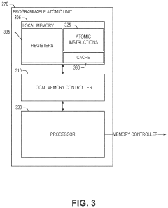
Method of organizing a programmable atomic unit instruction memory
PatentActiveUS20230195348A1
Innovation
- Storing instructions for programmable atomic transactions in the memory of the programmable atomic unit prior to execution, allowing them to be ready for immediate execution when requested, thereby reducing latency.
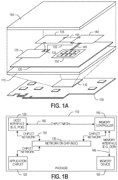
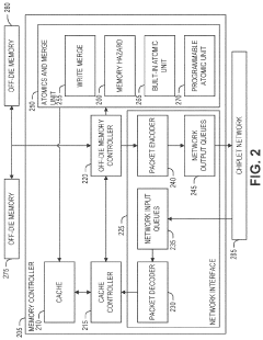
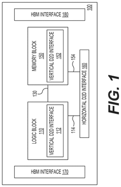
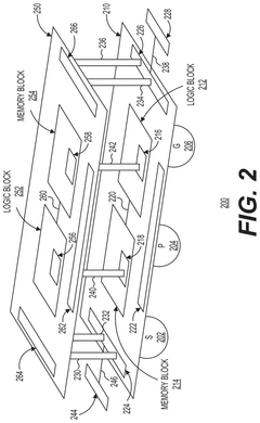
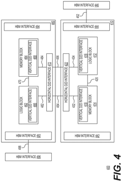
Homogeneous chiplets configurable as a two-dimensional system or a three-dimensional system
PatentPendingUS20250038120A1
Innovation
- A homogeneous chiplet system is introduced, comprising vertically stacked or horizontally coupled chiplets with on-die interconnect structures and vertical die-to-die interconnection structures, allowing for efficient data signal transfer and reducing latency.
Chiplet Integration Challenges
Chiplet integration presents several significant challenges that must be addressed to fully realize the potential of this innovative approach in computational methodologies. One of the primary obstacles is the development of efficient and reliable interconnect technologies. As chiplets are separate dies that need to communicate with each other, the interconnect between them becomes crucial for overall system performance. Current solutions, such as silicon interposers and advanced packaging techniques, still face limitations in terms of bandwidth, latency, and power efficiency.
Another major challenge lies in the thermal management of chiplet-based systems. With multiple dies in close proximity, heat dissipation becomes more complex compared to traditional monolithic designs. Ensuring uniform heat distribution and preventing thermal hotspots requires advanced cooling solutions and careful thermal design considerations. This challenge is further compounded by the increasing power densities of modern high-performance computing applications.
The design and verification of chiplet-based systems also pose significant hurdles. Integrating multiple chiplets from different vendors or process nodes requires sophisticated design methodologies and tools. Ensuring compatibility, managing signal integrity, and optimizing system-level performance become more intricate tasks. Additionally, the verification process becomes more complex, as interactions between chiplets must be thoroughly tested to guarantee reliable operation.
Manufacturing and testing of chiplet-based systems present their own set of challenges. Achieving high yields and maintaining consistent quality across multiple chiplets can be difficult, especially when dealing with heterogeneous integration. The assembly process requires precise alignment and bonding techniques to ensure proper connections between chiplets. Furthermore, testing chiplet-based systems demands new approaches to identify and isolate faults across multiple dies.
Standardization is another critical challenge in chiplet integration. The lack of widely adopted industry standards for chiplet interfaces and protocols hinders interoperability and limits the potential for mix-and-match approaches. Establishing common standards for chiplet design, integration, and testing is essential for fostering a robust ecosystem and enabling broader adoption of this technology.
Lastly, the economic aspects of chiplet integration pose challenges for widespread adoption. While chiplets offer potential cost benefits through improved yield and flexibility, the initial investment in new design tools, manufacturing processes, and testing equipment can be substantial. Balancing these costs with the potential benefits requires careful consideration and may impact the adoption rate across different market segments.
Chiplet Ecosystem Development
The Chiplet ecosystem has been rapidly evolving, driven by the need for more efficient and scalable computational solutions. This development is characterized by a complex interplay of technological advancements, industry collaborations, and standardization efforts.
At the core of the Chiplet ecosystem are the semiconductor manufacturers who are pioneering new packaging technologies. Companies like TSMC, Intel, and AMD have been at the forefront, developing advanced packaging solutions such as TSMC's Integrated Fan-Out (InFO) and Chip on Wafer on Substrate (CoWoS), Intel's Embedded Multi-die Interconnect Bridge (EMIB), and AMD's Infinity Fabric.
Complementing these efforts are the Electronic Design Automation (EDA) tool providers. Firms like Synopsys, Cadence, and Mentor Graphics have been developing specialized software tools to support Chiplet design, integration, and verification. These tools are crucial for managing the complexity of multi-die systems and ensuring optimal performance.
The ecosystem also includes IP providers who are developing reusable Chiplet designs and interface protocols. Companies like Arm, RISC-V International, and various startups are creating modular IP blocks that can be easily integrated into Chiplet-based systems, fostering innovation and reducing time-to-market for new products.
Standardization efforts play a vital role in the Chiplet ecosystem. Organizations such as the Open Compute Project (OCP) and JEDEC are working on developing open standards for Chiplet interfaces and packaging. These standards, like the Universal Chiplet Interconnect Express (UCIe), are crucial for ensuring interoperability between Chiplets from different vendors.
The ecosystem is further supported by packaging and testing companies. Firms like ASE Group, Amkor Technology, and JCET are developing advanced packaging solutions and testing methodologies specifically tailored for Chiplet-based designs.
Research institutions and universities are also contributing significantly to the ecosystem. They are exploring novel materials, interconnect technologies, and design methodologies that could shape the future of Chiplet technology.
As the ecosystem matures, we are seeing increased collaboration between different players. Joint ventures, strategic partnerships, and industry consortia are becoming more common, fostering innovation and accelerating the adoption of Chiplet technology across various computing domains.
Unlock deeper insights with Patsnap Eureka Quick Research — get a full tech report to explore trends and direct your research. Try now!
Generate Your Research Report Instantly with AI Agent
Supercharge your innovation with Patsnap Eureka AI Agent Platform!