

How to Facilitate Chiplet-Driven Rapid Prototyping?
JUL 16, 20259 MIN READ
Generate Your Research Report Instantly with AI Agent
Patsnap Eureka helps you evaluate technical feasibility & market potential.
Chiplet Technology Evolution and Objectives
Chiplet technology has emerged as a revolutionary approach in the semiconductor industry, offering a paradigm shift in chip design and manufacturing. The evolution of chiplet technology can be traced back to the early 2010s when the concept of disaggregating large monolithic chips into smaller, more manageable components began to gain traction. This evolution was driven by the increasing challenges in traditional chip scaling and the need for more flexible and cost-effective solutions.
The primary objective of chiplet technology is to overcome the limitations of Moore's Law by enabling the integration of heterogeneous components on a single package. This approach allows for the combination of different process nodes, intellectual property (IP) blocks, and even different materials within a single system. The goal is to achieve higher performance, improved power efficiency, and reduced costs compared to traditional monolithic designs.
In the context of rapid prototyping, chiplet technology aims to accelerate the development and testing of new chip designs. By leveraging pre-designed and pre-validated chiplets, designers can quickly assemble complex systems without the need to design every component from scratch. This modular approach significantly reduces time-to-market and allows for more iterative design processes.
The evolution of chiplet technology has been marked by several key milestones. Initially, the focus was on developing standardized interfaces and protocols to enable seamless communication between different chiplets. This led to the creation of industry standards such as the Advanced Interface Bus (AIB) and the Universal Chiplet Interconnect Express (UCIe).
As the technology matured, attention shifted towards improving packaging technologies to support high-density interconnects between chiplets. Advanced packaging solutions like 2.5D and 3D integration have become crucial enablers for chiplet-based designs, allowing for higher bandwidth and lower latency communication between components.
The objectives of chiplet technology in rapid prototyping are multifaceted. Firstly, it aims to reduce design complexity by allowing designers to focus on specific functional blocks rather than entire systems. Secondly, it seeks to improve design reusability, enabling companies to leverage existing IP across multiple products. Thirdly, it targets cost reduction by allowing the mix-and-match of components fabricated using different process nodes, optimizing the balance between performance and cost.
Looking forward, the objectives of chiplet technology include further standardization of interfaces and design methodologies to create a more robust ecosystem. There is also a push towards developing more sophisticated design tools and simulation environments that can accurately model the behavior of multi-chiplet systems. Additionally, research is ongoing to improve thermal management and power distribution in complex chiplet-based designs, which are critical factors in high-performance computing applications.
Market Demand for Rapid Prototyping Solutions
The market demand for rapid prototyping solutions in the chiplet-driven semiconductor industry has been experiencing significant growth in recent years. This surge is primarily driven by the increasing complexity of integrated circuits and the need for faster time-to-market in the highly competitive semiconductor landscape.
Chiplet technology has emerged as a game-changer in the semiconductor industry, allowing for more flexible and cost-effective chip designs. As a result, there is a growing demand for rapid prototyping solutions that can effectively leverage chiplet technology to accelerate the development and testing of new semiconductor products.
One of the key factors driving this demand is the need for faster iteration cycles in chip design. Traditional monolithic chip designs often require lengthy development and testing processes, which can be both time-consuming and expensive. Chiplet-driven rapid prototyping offers a solution to this challenge by enabling designers to quickly assemble and test different combinations of chiplets, significantly reducing development time and costs.
Furthermore, the increasing adoption of artificial intelligence and machine learning technologies across various industries has led to a surge in demand for specialized, high-performance computing solutions. Chiplet-based designs offer the flexibility to create custom-tailored solutions for specific AI and ML applications, driving the need for rapid prototyping tools that can facilitate the quick development and testing of these specialized chips.
The automotive industry, in particular, has shown a strong interest in chiplet-driven rapid prototyping solutions. As vehicles become more advanced and incorporate more electronic systems, there is a growing need for specialized semiconductor solutions. Rapid prototyping allows automotive manufacturers to quickly develop and test new chip designs for applications such as advanced driver assistance systems (ADAS) and autonomous driving technologies.
Another factor contributing to the market demand is the ongoing global chip shortage. This shortage has highlighted the need for more agile and flexible semiconductor manufacturing processes. Chiplet-driven rapid prototyping can help address this issue by enabling manufacturers to quickly develop and test new chip designs, potentially leading to more efficient use of manufacturing resources and faster time-to-market for new products.
The telecommunications industry, particularly with the rollout of 5G networks, is also driving demand for rapid prototyping solutions. The complex nature of 5G infrastructure requires specialized chip designs, and the ability to quickly prototype and test these designs is crucial for meeting the industry's aggressive deployment timelines.
Chiplet-Based Prototyping: Current State and Challenges
Chiplet-based prototyping represents a paradigm shift in the semiconductor industry, offering a modular approach to chip design and manufacturing. This methodology allows for the integration of multiple smaller chiplets onto a single package, enabling rapid prototyping and customization of complex systems-on-chip (SoCs). However, the current state of chiplet-based prototyping faces several challenges that need to be addressed to fully realize its potential.
One of the primary challenges is the lack of standardization in chiplet interfaces and protocols. While initiatives like Universal Chiplet Interconnect Express (UCIe) are making progress, the industry still lacks a universally adopted standard. This fragmentation hinders interoperability between chiplets from different vendors and complicates the integration process, limiting the flexibility and speed of prototyping efforts.
Another significant hurdle is the complexity of system-level design and verification. As chiplet-based designs involve multiple components from various sources, ensuring seamless integration and optimal performance becomes increasingly difficult. This challenge is compounded by the need for sophisticated tools and methodologies capable of handling the intricacies of multi-chiplet systems, including power management, thermal considerations, and signal integrity across chiplet boundaries.
The manufacturing and packaging processes for chiplet-based designs also present challenges. Advanced packaging technologies, such as 2.5D and 3D integration, are crucial for chiplet implementation but are still evolving. The yield and cost implications of these advanced packaging techniques can impact the viability of chiplet-based prototyping, especially for smaller companies or research institutions with limited resources.
Testing and validation of chiplet-based prototypes pose unique challenges as well. Traditional testing methodologies may not be sufficient to address the complexities introduced by multi-chiplet designs. Developing comprehensive test strategies that can effectively verify the functionality and performance of individual chiplets, as well as their interactions within the integrated system, remains a significant challenge.
Furthermore, the ecosystem for chiplet-based design and prototyping is still in its nascent stages. There is a need for more robust design tools, simulation environments, and manufacturing capabilities specifically tailored to chiplet-based approaches. The limited availability of these resources can slow down the adoption and effectiveness of chiplet-driven rapid prototyping.
Lastly, intellectual property (IP) management and security concerns present additional challenges in the chiplet ecosystem. As chiplet-based designs often involve components from multiple vendors, ensuring the protection of proprietary IP and maintaining security throughout the supply chain becomes more complex. This challenge can potentially hinder collaboration and slow down the prototyping process.
Existing Chiplet-Driven Prototyping Methodologies
01 Chiplet-based rapid prototyping systems
Rapid prototyping systems utilizing chiplets for faster and more efficient prototype development. These systems integrate modular chiplets to create customizable and scalable prototypes, allowing for quick iterations and reduced time-to-market for new products.- Chiplet-based rapid prototyping systems: Rapid prototyping systems utilizing chiplets for faster and more efficient prototype creation. These systems integrate modular semiconductor components to enable quick assembly and testing of complex electronic designs, reducing development time and costs in the prototyping process.
- 3D printing techniques for chiplet integration: Advanced 3D printing methods applied to chiplet-driven rapid prototyping, allowing for the creation of custom interconnects and packaging solutions. This approach enables the rapid fabrication of complex multi-chip modules and system-in-package designs.
- Software tools for chiplet-based design and simulation: Specialized software platforms developed for designing, simulating, and optimizing chiplet-based systems. These tools facilitate rapid virtual prototyping, enabling designers to evaluate various chiplet configurations and predict system performance before physical implementation.
- Thermal management solutions for chiplet prototypes: Innovative cooling techniques and thermal management strategies tailored for chiplet-based rapid prototypes. These solutions address the unique thermal challenges posed by densely packed chiplet arrangements, ensuring reliable operation during the prototyping phase.
- Automated assembly and testing of chiplet prototypes: Automated systems and methodologies for assembling and testing chiplet-based prototypes. These approaches incorporate advanced robotics and machine vision to streamline the integration of multiple chiplets, accelerating the prototyping process and improving reliability.
02 3D printing techniques for chiplet prototyping
Advanced 3D printing methods tailored for chiplet-based prototyping, enabling the creation of complex, multi-material structures. These techniques allow for rapid fabrication of chiplet housings, interconnects, and supporting structures, facilitating faster prototype assembly and testing.Expand Specific Solutions03 Chiplet interconnect and packaging solutions
Innovative interconnect and packaging technologies designed specifically for chiplet-based rapid prototyping. These solutions address challenges in chiplet integration, thermal management, and signal integrity, enabling more robust and reliable prototype designs.Expand Specific Solutions04 Software tools for chiplet-driven prototype design
Specialized software platforms and tools developed to support chiplet-based rapid prototyping workflows. These tools facilitate chiplet selection, placement, and integration, as well as performance simulation and optimization of chiplet-based prototype designs.Expand Specific Solutions05 Automated assembly systems for chiplet prototypes
Robotic and automated assembly systems tailored for chiplet-based prototype production. These systems enable high-precision placement and bonding of chiplets, reducing manual labor and improving consistency in prototype assembly.Expand Specific Solutions
Key Players in Chiplet and Rapid Prototyping Industries
The chiplet-driven rapid prototyping market is in its early growth stage, characterized by increasing adoption and technological advancements. The market size is expanding rapidly, driven by the demand for more efficient and flexible semiconductor design processes. Technologically, the field is evolving quickly, with companies like Intel, GlobalFoundries, and Micron Technology leading the way. These firms are developing advanced chiplet technologies, interconnect solutions, and integration methodologies. While the concept is promising, challenges remain in standardization and interoperability. Other players like AMD and Cadence Design Systems are also contributing significantly to the ecosystem, focusing on design tools and manufacturing processes to enable seamless chiplet integration and rapid prototyping capabilities.
Micron Technology, Inc.
Technical Solution: Micron's approach to chiplet-driven rapid prototyping focuses on memory-centric architectures and advanced packaging technologies. Their Hybrid Memory Cube (HMC) technology, while not strictly a chiplet approach, demonstrates their capability in 3D stacking and high-bandwidth memory interfaces, which are crucial for chiplet integration[9]. Micron's work on heterogeneous memory architectures and their development of high-bandwidth memory (HBM) products align well with chiplet-based designs. Their advanced packaging capabilities, including through-silicon vias (TSVs) and silicon interposers, enable the integration of memory chiplets with logic dies. Micron's involvement in the Open Compute Project's Open Domain-Specific Architecture (ODSA) subproject contributes to the development of open standards for chiplet interfaces, potentially accelerating the adoption of chiplet-based rapid prototyping[10].
Strengths: Expertise in memory technologies and advanced packaging, involvement in open standards development. Weaknesses: Primary focus on memory may limit broader system-level prototyping capabilities.
GLOBALFOUNDRIES, Inc.
Technical Solution: GLOBALFOUNDRIES' approach to chiplet-driven rapid prototyping leverages their diverse manufacturing capabilities and advanced packaging solutions. Their 2.5D and 3D integration technologies, including silicon interposers and through-silicon vias (TSVs), enable the efficient combination of chiplets in a single package[7]. GF's modular platform approach allows for rapid integration of different IP blocks, facilitating quick prototyping of complex systems. Their FDXcelerator Program provides a comprehensive suite of tools, IP, and reference designs to accelerate time-to-market for chiplet-based designs. GF's collaboration with packaging partners and their in-house advanced packaging capabilities support a wide range of chiplet integration options. Additionally, their GF Labs initiative focuses on developing new materials and integration schemes, potentially enabling more advanced chiplet prototyping capabilities in the future[8].
Strengths: Wide range of process nodes and packaging options, strong ecosystem partnerships. Weaknesses: Less vertical integration compared to IDMs, potentially longer turnaround times for full system prototypes.
Innovative Chiplet Interconnect Technologies
High-yield fabrication of large-format substrates with distributed, independent control elements
PatentActiveUS20120228669A1
Innovation
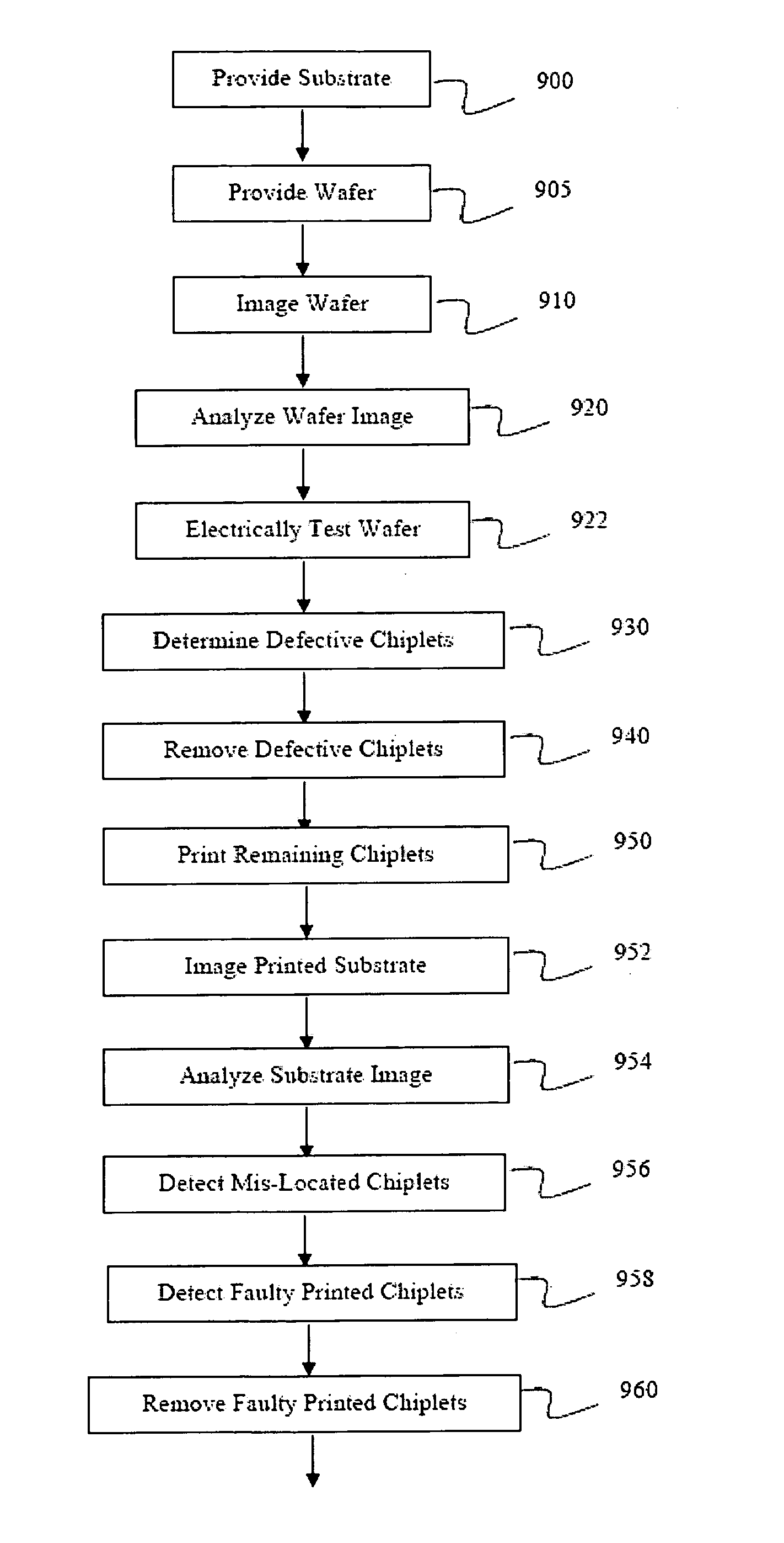
- A method involving the imaging and analysis of chiplets on a wafer to identify and remove defective ones, followed by printing remaining chiplets onto a substrate and replacing any missing or faulty ones from the same or different wafers, ensuring precise placement and functionality, thereby improving substrate quality and yield.
Rapid prototyping, generating and dynamically modifying a schema representing a database
PatentActiveUS7693918B2
Innovation
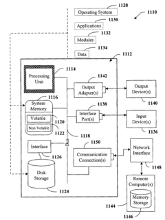
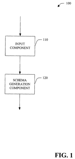
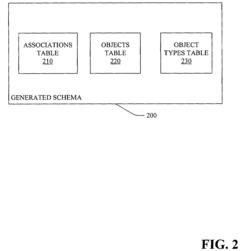
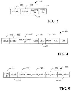
- A system and method for generating a database schema based on three main tables: object types, objects, and associations, allowing for dynamic modification and extension without hard-coding associations, enabling rapid prototyping and compatibility with prior versions.
Supply Chain Considerations for Chiplet Ecosystems
The supply chain for chiplet ecosystems is a critical factor in facilitating chiplet-driven rapid prototyping. As the semiconductor industry shifts towards disaggregated chip designs, the complexity of the supply chain increases, requiring careful consideration and management. One of the primary challenges is ensuring the availability and compatibility of diverse chiplets from multiple suppliers. This necessitates the establishment of standardized interfaces and protocols to enable seamless integration of chiplets from different sources.
Inventory management becomes more intricate in a chiplet-based ecosystem. Manufacturers must maintain a diverse stock of chiplets to support rapid prototyping efforts, balancing the need for variety with the risk of obsolescence. This requires sophisticated forecasting and just-in-time inventory systems to minimize costs while ensuring the availability of necessary components.
Quality control and testing procedures must be adapted to accommodate the unique challenges of chiplet-based designs. Each chiplet must be rigorously tested not only for individual performance but also for compatibility with other chiplets in the ecosystem. This may necessitate the development of new testing methodologies and equipment specifically tailored to chiplet integration.
Logistics and transportation considerations are also crucial in the chiplet supply chain. The fragile nature of these components demands specialized packaging and handling procedures to prevent damage during transit. Additionally, the global nature of the semiconductor industry requires efficient cross-border shipping solutions that can navigate complex international regulations and customs procedures.
Supplier relationships take on increased importance in a chiplet ecosystem. Manufacturers must cultivate a network of reliable chiplet suppliers, often entering into long-term partnerships to ensure consistent quality and supply. This may involve collaborative research and development efforts to drive innovation and address emerging challenges in chiplet technology.
The supply chain must also be resilient to disruptions, such as natural disasters, geopolitical tensions, or pandemics. Diversifying suppliers across different geographical regions can help mitigate risks, but it also adds complexity to supply chain management. Advanced analytics and artificial intelligence can play a crucial role in predicting and responding to potential disruptions, enabling more agile and robust supply chain strategies.
Standardization Efforts in Chiplet Technologies
Standardization efforts in chiplet technologies are crucial for facilitating chiplet-driven rapid prototyping. These efforts aim to establish common interfaces, protocols, and design methodologies that enable seamless integration of diverse chiplets from different vendors. The development of industry-wide standards is essential for creating a robust ecosystem that supports rapid prototyping and accelerates time-to-market for chiplet-based systems.
One of the most significant standardization initiatives is the Universal Chiplet Interconnect Express (UCIe) consortium. UCIe focuses on defining a die-to-die interconnect standard that allows chiplets from various manufacturers to communicate effectively. This standard encompasses physical layer specifications, protocol stack definitions, and software abstractions, providing a comprehensive framework for chiplet integration.
Another important standardization effort is the Open Compute Project's (OCP) Chiplet Design Exchange (CDX) initiative. CDX aims to create an open ecosystem for chiplet-based designs by developing standardized chiplet models, design methodologies, and verification processes. This initiative facilitates the exchange of chiplet designs between different organizations, promoting collaboration and accelerating innovation in the field.
The CHIPS Alliance, an open-source hardware initiative, is also contributing to chiplet standardization efforts. They are working on developing open-source tools and methodologies for chiplet design and integration, which can significantly reduce the barriers to entry for chiplet-based rapid prototyping.
In addition to these consortia-led efforts, individual companies are also contributing to standardization. For instance, Intel's Advanced Interface Bus (AIB) and AMD's Infinity Fabric are proprietary interconnect technologies that have been made available for wider industry adoption, potentially serving as de facto standards for chiplet integration.
Standardization efforts also extend to packaging technologies, which are critical for chiplet integration. The Joint Electron Device Engineering Council (JEDEC) is working on standards for advanced packaging technologies like 2.5D and 3D integration, which are essential for chiplet-based designs.
These standardization initiatives are collectively driving the chiplet ecosystem towards greater interoperability and modularity. By establishing common interfaces and protocols, they are enabling a more flexible and efficient approach to system design, where chiplets from different vendors can be easily mixed and matched to create custom solutions. This standardization is key to realizing the full potential of chiplet-driven rapid prototyping, allowing designers to quickly assemble and test complex systems using pre-validated chiplet building blocks.
Unlock deeper insights with Patsnap Eureka Quick Research — get a full tech report to explore trends and direct your research. Try now!
Generate Your Research Report Instantly with AI Agent
Supercharge your innovation with Patsnap Eureka AI Agent Platform!