Chiplet Impact on Next-Gen Signal Processing Techniques
JUL 16, 20259 MIN READ
Generate Your Research Report Instantly with AI Agent
Patsnap Eureka helps you evaluate technical feasibility & market potential.
Chiplet Technology Evolution and Objectives
Chiplet technology has emerged as a revolutionary approach in the semiconductor industry, fundamentally changing the way we design and manufacture integrated circuits. The evolution of chiplets can be traced back to the early 2010s when traditional monolithic chip designs began to face significant challenges in terms of scalability, yield, and cost-effectiveness. As Moore's Law slowed down, chiplets offered a promising solution to continue advancing computational power and efficiency.
The primary objective of chiplet technology is to disaggregate complex system-on-chip (SoC) designs into smaller, more manageable components that can be manufactured separately and then integrated onto a single package. This approach allows for greater flexibility in design, improved yield, and the ability to mix and match different process nodes for optimal performance and cost.
In the context of signal processing techniques, chiplets have opened up new possibilities for enhancing performance and efficiency. By separating analog and digital components, chiplet designs can optimize each element for its specific function, leading to improved signal integrity and reduced noise. This is particularly crucial for next-generation signal processing applications that demand high-speed data conversion and complex digital signal processing.
The evolution of chiplet technology has been marked by several key milestones. Initially, the focus was on developing reliable interconnect technologies to enable high-bandwidth, low-latency communication between chiplets. This led to the development of advanced packaging technologies such as silicon interposers and through-silicon vias (TSVs). Subsequently, industry standards like Universal Chiplet Interconnect Express (UCIe) have emerged to facilitate interoperability and accelerate adoption.
Looking ahead, the objectives for chiplet technology in signal processing applications are multifaceted. One primary goal is to further reduce power consumption while increasing processing capabilities, enabling more efficient edge computing and AI-driven signal processing. Another objective is to improve the integration of heterogeneous components, allowing for seamless combination of analog front-ends, digital signal processors, and AI accelerators within a single package.
Additionally, there is a strong focus on enhancing the scalability and modularity of chiplet-based designs. This will enable more rapid development of customized solutions for specific signal processing applications, from 5G and beyond communications to advanced radar and imaging systems. As chiplet technology continues to mature, we can expect to see increasingly sophisticated signal processing techniques that leverage the unique advantages of this disaggregated approach to chip design.
Market Demand for Advanced Signal Processing
The market demand for advanced signal processing techniques has been experiencing significant growth, driven by the increasing complexity of data processing requirements across various industries. As chiplet technology emerges as a game-changer in semiconductor design, its impact on next-generation signal processing techniques is becoming increasingly apparent, further fueling market demand.
The telecommunications sector, particularly with the rollout of 5G and the anticipation of 6G networks, is a major driver for advanced signal processing solutions. These networks require sophisticated algorithms for beamforming, massive MIMO, and spectrum efficiency, all of which benefit from the enhanced processing capabilities offered by chiplet-based designs. The demand for high-performance, energy-efficient signal processing in mobile devices and base stations is pushing the market towards more advanced solutions.
In the automotive industry, the rise of autonomous vehicles and advanced driver assistance systems (ADAS) is creating a substantial need for real-time signal processing. Chiplet technology enables the integration of multiple specialized processors, allowing for more efficient handling of sensor fusion, computer vision, and decision-making algorithms. This trend is expected to accelerate as vehicles become increasingly connected and autonomous.
The consumer electronics market is another significant contributor to the demand for advanced signal processing. High-definition audio and video processing, augmented and virtual reality applications, and AI-powered personal assistants all require sophisticated signal processing capabilities. Chiplet-based designs offer the potential for more powerful and energy-efficient consumer devices, driving market growth in this sector.
In the industrial and manufacturing sectors, the adoption of Industry 4.0 principles is leading to increased demand for advanced signal processing in areas such as predictive maintenance, quality control, and process optimization. The ability of chiplet technology to combine different types of processors and accelerators is particularly valuable in these applications, where a mix of real-time processing and complex analytics is often required.
The healthcare industry is also emerging as a significant market for advanced signal processing techniques. Medical imaging, biosignal analysis, and AI-assisted diagnostics all benefit from the improved processing capabilities offered by chiplet-based designs. As healthcare becomes increasingly data-driven and personalized, the demand for sophisticated signal processing solutions is expected to grow substantially.
The market for advanced signal processing is further bolstered by the growing importance of edge computing and the Internet of Things (IoT). These paradigms require distributed processing capabilities that can handle complex algorithms with low latency and high energy efficiency – characteristics that align well with the strengths of chiplet technology.
Chiplet Challenges in Signal Processing
The integration of chiplets into signal processing systems presents several significant challenges that must be addressed to fully leverage their potential. One of the primary obstacles is the interconnect bottleneck between chiplets. As signal processing applications demand increasingly higher bandwidth and lower latency, the inter-chiplet communication becomes a critical limiting factor. Traditional packaging technologies struggle to provide the necessary data rates and signal integrity required for advanced signal processing algorithms.
Another challenge lies in the thermal management of chiplet-based signal processing systems. The high-performance nature of signal processing applications often results in substantial heat generation. When multiple chiplets are integrated into a single package, the thermal density increases dramatically, potentially leading to hotspots and performance degradation. Effective heat dissipation strategies must be developed to ensure optimal performance and reliability of chiplet-based signal processing solutions.
Power distribution and management across multiple chiplets pose additional challenges. Signal processing algorithms often require precise timing and synchronization, which can be disrupted by voltage fluctuations or power delivery inconsistencies across different chiplets. Designing efficient power delivery networks that can maintain stable voltage levels across all chiplets is crucial for ensuring the accuracy and reliability of signal processing operations.
The heterogeneous integration of chiplets also introduces challenges in terms of design complexity and verification. Signal processing systems may require the integration of chiplets fabricated using different process nodes or even different semiconductor technologies. Ensuring compatibility and optimal performance across these diverse components demands sophisticated design methodologies and extensive verification processes.
Furthermore, the chiplet approach introduces new considerations for signal integrity and electromagnetic interference (EMI) management. The increased number of high-speed interfaces between chiplets can lead to signal degradation and crosstalk, potentially impacting the accuracy of signal processing operations. Careful design of package substrates, signal routing, and shielding is necessary to mitigate these issues and maintain the fidelity of processed signals.
Lastly, the adoption of chiplets in signal processing applications faces challenges related to standardization and ecosystem development. The lack of widely accepted standards for chiplet interfaces and integration methodologies can hinder interoperability and limit the potential for mix-and-match approaches. Establishing industry-wide standards and fostering a robust ecosystem of chiplet suppliers and integrators is essential for realizing the full benefits of chiplet technology in next-generation signal processing systems.
Current Chiplet-based Signal Processing Solutions
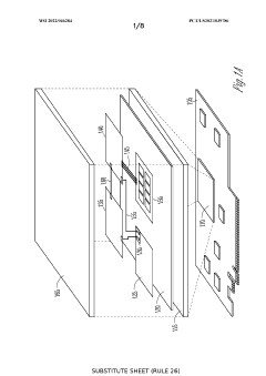
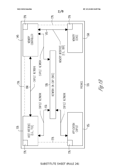
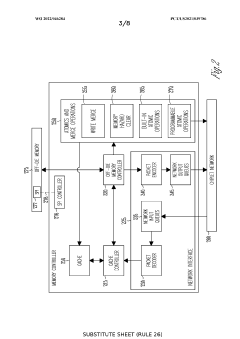
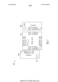
01 Chiplet interconnect and signal processing
This approach focuses on the interconnection and signal processing between multiple chiplets in a system. It involves techniques for managing high-speed data transfer, signal integrity, and communication protocols between different chiplets. The methods aim to optimize performance and reduce latency in multi-chiplet architectures.- Chiplet interconnect and signal processing: This approach focuses on optimizing signal processing and communication between multiple chiplets in a system. It involves developing efficient interconnect technologies and protocols to enable high-speed, low-latency data transfer between chiplets. Advanced signal processing techniques are employed to maintain signal integrity across chiplet boundaries and reduce interference.
- Heterogeneous chiplet integration for signal processing: This method involves integrating diverse chiplets with different functionalities, such as analog, digital, and mixed-signal processing capabilities. The integration allows for specialized signal processing tasks to be distributed across multiple chiplets, optimizing overall system performance and power efficiency. Techniques for managing the complexities of heterogeneous integration, including thermal management and power distribution, are key aspects of this approach.
- AI and machine learning for chiplet-based signal processing: This innovation incorporates artificial intelligence and machine learning algorithms into chiplet-based signal processing systems. These techniques are used to optimize signal routing, enhance signal quality, and adapt to changing conditions in real-time. The approach leverages the distributed nature of chiplet architectures to implement efficient, scalable AI-driven signal processing solutions.
- 3D chiplet stacking for enhanced signal processing: This technique utilizes three-dimensional stacking of chiplets to create compact, high-performance signal processing systems. The vertical integration allows for shorter interconnects, reduced signal latency, and improved thermal management. Advanced through-silicon via (TSV) technology and die-to-die bonding methods are employed to enable efficient signal transmission between stacked chiplets.
- Reconfigurable chiplet architectures for adaptive signal processing: This approach focuses on developing chiplet-based systems with reconfigurable architectures that can adapt to varying signal processing requirements. It involves the use of programmable interconnects and flexible processing elements that can be dynamically reconfigured based on the specific signal processing tasks at hand. This adaptability allows for optimized performance across a wide range of applications and operating conditions.
02 Power management and thermal control in chiplet systems
This category addresses power distribution, management, and thermal control strategies for chiplet-based designs. It includes techniques for efficient power delivery to individual chiplets, dynamic power management across the system, and thermal management solutions to ensure optimal performance and reliability of chiplet architectures.Expand Specific Solutions03 Chiplet-based AI and machine learning acceleration
This area focuses on leveraging chiplet technology for artificial intelligence and machine learning applications. It includes specialized chiplet designs for AI processing, efficient data flow architectures between chiplets for neural network computations, and optimization techniques for AI workloads in multi-chiplet systems.Expand Specific Solutions04 3D integration and packaging for chiplet systems
This point covers advanced packaging and 3D integration techniques for chiplet-based designs. It includes methods for vertical stacking of chiplets, through-silicon via (TSV) technology, and innovative packaging solutions to improve density, performance, and thermal management in chiplet architectures.Expand Specific Solutions05 Chiplet-based memory systems and cache coherency
This category addresses memory architectures and cache coherency protocols specifically designed for chiplet-based systems. It includes techniques for efficient memory access across multiple chiplets, innovative cache designs, and methods to maintain coherency in distributed cache systems within a chiplet architecture.Expand Specific Solutions
Key Players in Chiplet and Signal Processing
The chiplet technology's impact on next-generation signal processing techniques is at a pivotal stage of development, with the market poised for significant growth. The industry is transitioning from early adoption to more widespread implementation, driven by the need for improved performance and energy efficiency in complex computing systems. The global market for chiplet-based solutions is expanding rapidly, with projections indicating substantial growth in the coming years. Technologically, while still evolving, chiplets are gaining maturity, with companies like AMD, Intel, and TSMC leading the charge. These firms, along with others such as Micron Technology and MediaTek, are investing heavily in research and development to overcome integration challenges and standardize interfaces, pushing the boundaries of what's possible in signal processing applications.
MediaTek, Inc.
Technical Solution: MediaTek's approach to chiplet-based signal processing focuses on integrating diverse functionalities for mobile and IoT devices. They are developing modular chiplet designs that combine their AI processing units, 5G modems, and multimedia engines. MediaTek's strategy involves using advanced packaging technologies like InFO (Integrated Fan-Out) and CoWoS (Chip-on-Wafer-on-Substrate) to create compact, power-efficient SoCs[9]. For next-gen signal processing, MediaTek is exploring heterogeneous integration, combining chiplets manufactured at different process nodes to optimize performance and cost. Their APU (AI Processing Unit) technology, for instance, is being developed as a separate chiplet that can be easily integrated with their Dimensity 5G SoCs, enabling flexible configurations for different market segments[10].
Strengths: Strong presence in mobile and IoT markets, experience in integrating diverse functionalities, cost-effective solutions. Weaknesses: Less prominence in high-performance computing markets, potential challenges in competing with larger rivals in advanced packaging technologies.
Advanced Micro Devices, Inc.
Technical Solution: AMD's chiplet strategy for next-gen signal processing centers around their Infinity Fabric interconnect technology. This approach allows AMD to combine multiple smaller dies (chiplets) manufactured using advanced process nodes for core functionality, with I/O and other components on separate dies using mature processes. For signal processing applications, AMD is developing specialized chiplets that can be integrated with their CPU and GPU cores. Their CDNA architecture for AI and HPC workloads, for example, uses chiplet-based design to achieve high performance and efficiency[3]. AMD's chiplets are designed to work seamlessly together, with a coherent memory subsystem that enables efficient data sharing between different processing elements[4].
Strengths: Cost-effective manufacturing, ability to mix-and-match different process nodes, high performance in multi-chip configurations. Weaknesses: Potential latency issues between chiplets, complexity in thermal management of multi-chip packages.
Innovative Chiplet Interconnect Technologies
Method for configuring multiple input-output channels
PatentWO2022046284A1
Innovation
- The implementation of a Chiplet Protocol Interface (CPI) network with Advanced Interface Bus (AIB) channels and credit-based flow control, allowing for flexible virtual channel mapping and minimizing latency and energy consumption through packetized protocols and serialization-deserialization (SERDES) hardware, while enabling efficient inter-chiplet communication.
Data flow in a distributed graphics processing unit architecture
PatentActiveUS20210158599A1
Innovation
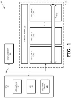
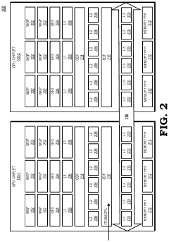
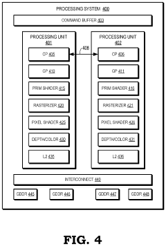
- A distributed architecture using chiplets with high-performance interconnection, where geometry and pixel workloads are processed by multiple processing units with duplicated fixed function hardware blocks and shaders, and a shared coherent cache, allowing for checkerboarding of pixel processing across units to manage synchronization and bandwidth effectively.
Thermal Management in Chiplet Designs
Thermal management has become a critical challenge in chiplet designs, particularly as the demand for higher performance and increased integration continues to grow. The modular nature of chiplets introduces unique thermal considerations that must be addressed to ensure optimal system performance and reliability.
One of the primary thermal challenges in chiplet designs is the increased power density resulting from the close proximity of multiple high-performance dies. As chiplets are packed tightly together, the heat generated by each component can accumulate rapidly, leading to potential hotspots and thermal throttling. This issue is further exacerbated by the varying thermal characteristics of different chiplets within a single package.
To address these challenges, several innovative thermal management techniques have been developed specifically for chiplet architectures. Advanced packaging technologies, such as silicon interposers and through-silicon vias (TSVs), play a crucial role in facilitating efficient heat dissipation. These technologies enable better thermal coupling between chiplets and the package substrate, allowing for more effective heat spreading.
Active cooling solutions have also been adapted for chiplet designs. Liquid cooling systems, for instance, can be integrated directly into the interposer or package substrate, providing targeted cooling to high-power chiplets. This approach allows for more precise temperature control and can significantly reduce thermal gradients across the package.
Another promising approach is the use of thermally aware floorplanning and chiplet placement. By strategically positioning high-power chiplets and incorporating thermal buffer zones, designers can optimize heat distribution and minimize thermal hotspots. This technique often involves sophisticated thermal modeling and simulation to predict and mitigate potential thermal issues before fabrication.
The development of advanced thermal interface materials (TIMs) has also contributed to improved thermal management in chiplet designs. These materials, designed to fill the microscopic gaps between chiplets and heat spreaders, offer enhanced thermal conductivity and reduced thermal resistance. Some cutting-edge TIMs incorporate phase-change materials or nanoparticles to further improve heat transfer efficiency.
Looking ahead, emerging technologies such as on-chip thermoelectric coolers and microfluidic cooling channels integrated directly into chiplets show promise for next-generation thermal management solutions. These innovations could enable even more precise and localized cooling, potentially unlocking new levels of performance and integration in chiplet-based systems.
As chiplet designs continue to evolve, thermal management will remain a critical area of focus for researchers and engineers. The development of more sophisticated thermal modeling tools, coupled with advancements in materials science and cooling technologies, will be essential in addressing the thermal challenges posed by increasingly complex and powerful chiplet architectures.
Standardization Efforts for Chiplet Ecosystems
The standardization efforts for chiplet ecosystems are crucial for the widespread adoption and integration of chiplet technology in next-generation signal processing techniques. These efforts aim to establish common protocols, interfaces, and design methodologies that enable interoperability between chiplets from different manufacturers.
One of the primary standardization initiatives is the Universal Chiplet Interconnect Express (UCIe), which focuses on creating a unified interconnect standard for chiplets. UCIe defines the physical and protocol layers for die-to-die interconnects, ensuring seamless communication between chiplets. This standard is backed by major industry players, including Intel, AMD, Arm, and TSMC, highlighting its potential to become the de facto standard for chiplet interconnects.
Another significant standardization effort is the Open Compute Project's (OCP) Chiplet Design Exchange (CDX) format. CDX aims to standardize the exchange of chiplet design information between different tools and organizations. This format facilitates the creation of a more open and collaborative chiplet ecosystem, enabling faster innovation and reducing time-to-market for chiplet-based products.
The JEDEC Solid State Technology Association is also contributing to chiplet standardization through its JC-70 Committee for Wide I/O Memories. This committee is developing standards for high-bandwidth memory interfaces, which are critical for chiplet-based designs in signal processing applications.
In addition to these industry-led efforts, academic institutions and research organizations are collaborating on standardization initiatives. For example, the European Chip Initiative (ECI) is working on developing open standards for chiplet-based systems, with a focus on European semiconductor independence and competitiveness.
Standardization efforts also extend to packaging technologies, which are essential for chiplet integration. The Heterogeneous Integration Roadmap (HIR), sponsored by IEEE, SEMI, and other organizations, provides a comprehensive framework for advancing packaging technologies and standards for chiplet-based systems.
These standardization efforts are expected to accelerate the adoption of chiplet technology in signal processing applications by reducing design complexity, improving interoperability, and lowering costs. As these standards mature, they will enable more efficient and flexible system designs, paving the way for innovative signal processing techniques that leverage the advantages of chiplet architecture.
Unlock deeper insights with Patsnap Eureka Quick Research — get a full tech report to explore trends and direct your research. Try now!
Generate Your Research Report Instantly with AI Agent
Supercharge your innovation with Patsnap Eureka AI Agent Platform!