How to Optimize Chiplet Circuit Connectivity for High-Speed Devices?
JUL 16, 20259 MIN READ
Generate Your Research Report Instantly with AI Agent
Patsnap Eureka helps you evaluate technical feasibility & market potential.
Chiplet Connectivity Evolution and Objectives
Chiplet technology has emerged as a revolutionary approach in the semiconductor industry, addressing the challenges of traditional monolithic chip designs. The evolution of chiplet connectivity has been driven by the increasing demand for higher performance, lower power consumption, and improved scalability in modern computing systems.
The journey of chiplet connectivity began with the concept of multi-chip modules (MCMs) in the 1980s. These early implementations used traditional packaging technologies to connect multiple dies on a single substrate. As technology progressed, more advanced interconnect solutions were developed, such as silicon interposers and through-silicon vias (TSVs), which enabled higher bandwidth and denser integration.
In recent years, the focus has shifted towards advanced packaging technologies like 2.5D and 3D integration. These approaches have significantly improved chiplet-to-chiplet communication, allowing for higher data rates and reduced latency. The introduction of die-to-die interfaces, such as Intel's EMIB (Embedded Multi-die Interconnect Bridge) and AMD's Infinity Fabric, has further enhanced the capabilities of chiplet-based designs.
The primary objective of chiplet connectivity optimization is to achieve seamless integration of multiple dies while maximizing performance and minimizing power consumption. This involves developing high-speed, low-latency interconnects that can support the increasing bandwidth requirements of modern applications. Additionally, there is a strong focus on improving signal integrity and reducing crosstalk between chiplets to ensure reliable communication.
Another crucial goal is to enhance the flexibility and modularity of chiplet designs. This includes developing standardized interfaces and protocols that allow for easier integration of chiplets from different vendors, promoting a more diverse and competitive ecosystem. The CHIPS Alliance and Open Compute Project are examples of industry initiatives working towards this objective.
Power efficiency is a key consideration in chiplet connectivity optimization. As data rates increase, so does the power consumption of interconnects. Therefore, developing energy-efficient signaling techniques and optimizing power delivery networks are essential objectives in the evolution of chiplet technology.
Looking ahead, the future objectives of chiplet connectivity include pushing the boundaries of integration density, exploring novel materials and packaging technologies, and developing advanced design and simulation tools. These efforts aim to enable the creation of highly complex, heterogeneous systems that can meet the demands of emerging applications in artificial intelligence, 5G communications, and high-performance computing.
High-Speed Device Market Analysis
The high-speed device market has experienced significant growth in recent years, driven by the increasing demand for faster and more efficient electronic systems across various industries. This market segment encompasses a wide range of products, including high-performance computing (HPC) systems, data centers, telecommunications equipment, and advanced consumer electronics.
The global high-speed device market is projected to continue its upward trajectory, with a compound annual growth rate (CAGR) expected to exceed 8% over the next five years. This growth is primarily fueled by the rapid adoption of 5G technology, the expansion of cloud computing services, and the increasing need for high-bandwidth applications in both consumer and enterprise sectors.
One of the key drivers of this market is the ever-increasing demand for data processing and transmission speeds. As the volume of data generated and consumed globally continues to surge, there is a growing need for devices capable of handling these massive data flows efficiently. This trend is particularly evident in the data center and HPC segments, where the push for exascale computing and AI-driven applications is driving the development of faster, more powerful chipsets.
The telecommunications sector is another major contributor to the high-speed device market growth. With the ongoing rollout of 5G networks worldwide, there is a substantial demand for high-speed devices capable of supporting the increased bandwidth and lower latency requirements of next-generation mobile networks. This includes not only consumer devices like smartphones and tablets but also network infrastructure equipment such as base stations and routers.
In the consumer electronics segment, the proliferation of high-resolution displays, virtual and augmented reality devices, and advanced gaming systems is creating a strong demand for high-speed processing and connectivity solutions. This trend is expected to continue as consumers increasingly seek more immersive and responsive digital experiences.
The automotive industry is emerging as a significant new market for high-speed devices, driven by the development of autonomous vehicles and advanced driver assistance systems (ADAS). These applications require powerful processing capabilities and high-speed connectivity to handle the vast amounts of sensor data and real-time decision-making involved in autonomous driving.
However, the high-speed device market also faces several challenges. One of the primary concerns is the increasing power consumption associated with higher processing speeds and data rates. This has led to a growing focus on energy-efficient designs and novel cooling solutions to address thermal management issues in high-performance devices.
Another challenge is the need for standardization and interoperability among different high-speed technologies and protocols. As the market continues to evolve, ensuring seamless integration and compatibility between various high-speed devices and systems will be crucial for widespread adoption and market growth.
Chiplet Interconnect Challenges
As chiplet technology continues to advance, the challenges associated with interconnecting these smaller, modular components become increasingly complex. One of the primary obstacles in optimizing chiplet circuit connectivity for high-speed devices lies in managing signal integrity across the interconnects. As data rates increase, maintaining signal quality becomes more difficult due to factors such as crosstalk, electromagnetic interference, and signal attenuation.
Another significant challenge is thermal management. The dense packaging of chiplets can lead to localized hot spots, which can negatively impact performance and reliability. Designing effective thermal solutions that can dissipate heat efficiently while maintaining the compact form factor of chiplet-based designs is a critical consideration.
Power delivery poses yet another hurdle in chiplet interconnect optimization. Ensuring consistent and adequate power supply to each chiplet, especially in high-performance applications, requires careful consideration of power distribution networks and decoupling strategies. The challenge is further compounded by the need to minimize power consumption and maximize energy efficiency.
Standardization and interoperability present additional challenges in the chiplet ecosystem. As different manufacturers produce chiplets with varying specifications and interfaces, ensuring seamless integration and communication between these components becomes crucial. The lack of universal standards for chiplet interconnects can hinder widespread adoption and limit the potential benefits of this technology.
Manufacturing and assembly processes also contribute to the complexity of chiplet interconnect optimization. Achieving precise alignment and bonding between chiplets and the interposer or substrate requires advanced packaging technologies. The yield and reliability of these connections directly impact the overall performance and cost-effectiveness of chiplet-based designs.
Bandwidth limitations and latency issues are persistent challenges in high-speed chiplet interconnects. As data rates continue to increase, traditional interconnect technologies may struggle to keep pace with the bandwidth requirements of advanced applications. Minimizing latency while maximizing data throughput is a delicate balance that designers must strike.
Lastly, the challenge of scalability looms large in chiplet interconnect design. As systems grow more complex and incorporate a larger number of chiplets, the interconnect architecture must be able to scale efficiently without compromising performance or reliability. This requires innovative approaches to routing, signaling, and system-level integration.
Current Chiplet Connectivity Solutions
01 Interconnect structures for chiplet connectivity
Advanced interconnect structures are developed to facilitate high-speed, high-bandwidth communication between chiplets. These structures may include through-silicon vias (TSVs), interposers, and advanced packaging technologies to enable efficient data transfer and power distribution across multiple chiplets in a single package.- Interconnect technologies for chiplet integration: Advanced interconnect technologies are crucial for chiplet integration, enabling high-speed and efficient communication between different chiplets. These technologies include through-silicon vias (TSVs), interposers, and advanced packaging solutions that facilitate seamless connectivity and data transfer between chiplets, enhancing overall system performance and reducing latency.
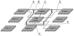
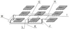
- Network-on-Chip (NoC) architectures for chiplets: Network-on-Chip architectures are being developed specifically for chiplet-based systems, providing scalable and flexible communication infrastructure. These NoC designs optimize data routing between chiplets, manage bandwidth allocation, and support various protocols to ensure efficient inter-chiplet connectivity across complex multi-chiplet configurations.
- 3D integration and stacking for chiplet connectivity: Three-dimensional integration and stacking techniques are being employed to enhance chiplet connectivity. These methods involve vertically stacking chiplets and utilizing advanced bonding technologies to create high-density interconnects. This approach minimizes signal travel distances, reduces power consumption, and enables more compact and efficient chiplet-based systems.
- Standardized interfaces for chiplet connectivity: The development of standardized interfaces for chiplet connectivity is gaining traction in the industry. These interfaces aim to establish common protocols and specifications for chiplet-to-chiplet communication, promoting interoperability and simplifying the integration of chiplets from different vendors. Standardization efforts focus on aspects such as physical layer designs, signaling methods, and communication protocols.
- Adaptive and reconfigurable chiplet interconnects: Research is ongoing in the area of adaptive and reconfigurable chiplet interconnects. These innovative approaches allow for dynamic adjustment of interconnect properties based on workload requirements, power constraints, or system conditions. Such flexibility enables optimized performance, improved energy efficiency, and enhanced fault tolerance in chiplet-based systems.
02 Chiplet-to-chiplet communication protocols
Specialized communication protocols are designed for chiplet-to-chiplet interactions, optimizing data transfer rates and reducing latency. These protocols may include custom signaling methods, error correction mechanisms, and synchronization techniques tailored for the unique requirements of chiplet-based architectures.Expand Specific Solutions03 Power management and distribution for chiplet systems
Innovative power management techniques are developed to efficiently distribute and regulate power across multiple chiplets. This includes advanced power gating, dynamic voltage and frequency scaling, and thermal management strategies to optimize performance and energy efficiency in chiplet-based designs.Expand Specific Solutions04 Chiplet integration and packaging technologies
Novel packaging technologies are created to integrate multiple chiplets into a single package. This includes advanced substrate designs, die-to-die bonding techniques, and 3D stacking methods to achieve high-density integration while maintaining reliable electrical and thermal connections between chiplets.Expand Specific Solutions05 Testing and verification methods for chiplet-based systems
Specialized testing and verification methodologies are developed to ensure the functionality and reliability of chiplet-based systems. This includes pre-silicon validation techniques, post-assembly testing procedures, and in-field diagnostics to identify and mitigate potential connectivity issues between chiplets.Expand Specific Solutions
Key Chiplet Industry Players
The optimization of chiplet circuit connectivity for high-speed devices is currently in a dynamic growth phase, with the market expanding rapidly due to increasing demand for advanced computing solutions. The global chiplet market is projected to reach significant scale in the coming years, driven by the need for improved performance and energy efficiency in various applications. Technologically, the field is progressing swiftly, with companies like Intel, QUALCOMM, and Huawei leading innovation. These industry giants, along with emerging players such as AvicenaTech Corp. and Rambus, are pushing the boundaries of chiplet interconnect technologies, focusing on ultra-dense, low-latency, and low-power solutions to address the challenges of high-speed device connectivity.
Intel Corp.
Technical Solution: Intel's approach to optimizing chiplet circuit connectivity for high-speed devices involves their advanced packaging technologies, particularly their Embedded Multi-die Interconnect Bridge (EMIB) and Foveros 3D packaging. EMIB uses a small silicon bridge embedded in the package substrate to connect multiple chiplets, allowing for high-bandwidth, short-reach interconnects[1]. This technology enables die-to-die connections with a pitch as low as 35 microns, significantly improving connectivity density[2]. Foveros, on the other hand, is a 3D packaging technology that allows for vertical stacking of chiplets, further enhancing connectivity and reducing the overall footprint[3]. Intel has also developed their AIB (Advanced Interface Bus) protocol, which is an open standard for die-to-die communication, supporting speeds up to 2 Gbps per pin[4].
Strengths: High bandwidth, reduced latency, and improved power efficiency. The open standard AIB protocol promotes industry-wide adoption. Weaknesses: Complexity in manufacturing and potential thermal management issues in 3D stacked designs.
QUALCOMM, Inc.
Technical Solution: Qualcomm's approach to chiplet connectivity optimization focuses on their 3D packaging technology and advanced heterogeneous integration. They have developed a chiplet-based design methodology called "3D-IC" that allows for the vertical stacking of multiple dies[1]. This approach utilizes Through-Silicon Vias (TSVs) and micro-bumps for inter-die connections, enabling high-bandwidth and low-latency communication between chiplets[2]. Qualcomm has also introduced their own die-to-die interface standard called "QTI Interface" which supports data rates up to 1.6 Tbps[3]. Additionally, they have implemented advanced signal integrity techniques, including equalization and pre-emphasis, to maintain signal quality at high speeds across chiplet interconnects[4].
Strengths: High bandwidth density, flexibility in integrating heterogeneous technologies, and reduced form factor. Weaknesses: Potential increased manufacturing costs and complexity in thermal management for 3D stacked designs.
Innovative Interconnect Technologies
Hybrid bonded interconnect bridging
PatentActiveUS12107075B2
Innovation
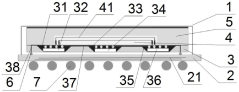
- The use of a hybrid bond, comprising a copper bond and an oxide bond, for direct interconnect die coupling to chiplets, enabling finer pitch connections less than 10 micrometers, along with trans-silicon via connections, conductive pillars, and fluorosilicate glass dielectric layers for improved signal transfer and power distribution.
A wafer-level reconfigurable chiplet integrated structure
PatentActiveCN114420681B
Innovation
- Adopting a wafer-level reconfigurable chiplet integrated structure, including tube shell, substrate, RDL, chamber, functional chiplet, reconfigurable topology network, through hole, chiplet communication network and other components, through the reconfigurable topology network and chiplet communication network The design enables flexible reconstruction and efficient integration of the system, avoiding problems in the traditional chip wire bonding process.
Thermal Management Strategies
Thermal management is a critical aspect of optimizing chiplet circuit connectivity for high-speed devices. As chiplets become more densely packed and operate at higher frequencies, the heat generated during operation poses significant challenges to performance and reliability. Effective thermal management strategies are essential to maintain optimal operating temperatures and ensure the longevity of these advanced devices.
One key approach to thermal management in chiplet-based systems is the implementation of advanced cooling solutions. These may include the use of high-performance thermal interface materials (TIMs) to improve heat transfer between the chiplets and the heat spreader. Additionally, innovative heat sink designs, such as micro-channel liquid cooling or vapor chamber technologies, can be employed to efficiently dissipate heat from the chiplets. These cooling solutions must be carefully integrated into the overall package design to maximize their effectiveness while minimizing their impact on signal integrity and power delivery.
Another important strategy is the optimization of chiplet placement and routing to minimize hotspots and improve overall thermal distribution. This involves careful consideration of the power density of each chiplet and strategic placement to ensure even heat distribution across the package. Advanced thermal modeling and simulation tools can be utilized to predict and optimize thermal performance during the design phase, allowing engineers to identify and address potential thermal issues before fabrication.
Power management techniques also play a crucial role in thermal management for high-speed chiplet-based devices. Implementing dynamic voltage and frequency scaling (DVFS) can help reduce power consumption and heat generation during periods of lower computational demand. Additionally, incorporating on-die thermal sensors and intelligent power management algorithms can enable real-time thermal monitoring and adaptive power control, ensuring that the device operates within safe temperature limits while maximizing performance.
The integration of thermally aware design methodologies throughout the chiplet development process is essential for optimizing thermal management. This includes considering thermal constraints during floorplanning, implementing thermal-aware routing algorithms, and incorporating thermal vias and other heat-dissipating structures into the chiplet and interposer designs. By addressing thermal considerations at every stage of the design process, engineers can create more thermally efficient and reliable high-speed chiplet-based devices.
Furthermore, the development of advanced packaging technologies, such as embedded cooling solutions and 3D stacking with through-silicon vias (TSVs), offers new opportunities for improving thermal management in chiplet-based systems. These innovative approaches allow for more efficient heat removal and can potentially enable even higher levels of integration and performance in future high-speed devices.
Chiplet Standards and Ecosystem
The development of chiplet technology has necessitated the establishment of robust standards and a thriving ecosystem to ensure interoperability and widespread adoption. Several industry consortia and organizations have emerged to address this need, with the Universal Chiplet Interconnect Express (UCIe) consortium leading the charge. UCIe aims to create an open industry standard for die-to-die interconnects, enabling seamless integration of chiplets from different vendors.
The UCIe specification defines both the physical and protocol layers for chiplet interconnects, covering aspects such as electrical signaling, physical design, and protocol stack. This standardization effort is crucial for fostering innovation and competition in the chiplet market, as it allows companies to focus on their core competencies while leveraging the expertise of others through modular chip design.
Alongside UCIe, other standards and initiatives have emerged to support the chiplet ecosystem. The Open Compute Project (OCP) has introduced the Open Domain-Specific Architecture (ODSA) subproject, which focuses on developing open architectures and specifications for chiplet-based systems. The ODSA aims to create a marketplace for chiplets, enabling a more diverse and competitive semiconductor industry.
The Advanced Interface Bus (AIB) standard, developed by Intel and now managed by the ODSA, provides another option for chiplet interconnects. AIB offers a flexible and scalable interface for die-to-die communication, supporting high-bandwidth and low-latency connections between chiplets.
As the chiplet ecosystem continues to evolve, collaboration between semiconductor manufacturers, packaging companies, and electronic design automation (EDA) tool providers is becoming increasingly important. This collaboration is driving the development of new design methodologies, verification techniques, and manufacturing processes tailored to chiplet-based architectures.
The ecosystem is also expanding to include specialized chiplet marketplaces and design libraries. These platforms aim to simplify the process of sourcing and integrating chiplets from multiple vendors, accelerating the development of complex systems-on-chip (SoCs) and reducing time-to-market for new products.
To support the growing chiplet ecosystem, advancements in packaging technologies are crucial. Innovations in 2.5D and 3D packaging, such as silicon interposers and through-silicon vias (TSVs), are enabling more sophisticated chiplet integration schemes. These packaging technologies are essential for realizing the full potential of chiplet-based designs, allowing for higher performance, lower power consumption, and improved thermal management.
Unlock deeper insights with Patsnap Eureka Quick Research — get a full tech report to explore trends and direct your research. Try now!
Generate Your Research Report Instantly with AI Agent
Supercharge your innovation with Patsnap Eureka AI Agent Platform!