

Emerging Trends in Chiplet Manufacturing Techniques
JUL 16, 20259 MIN READ
Generate Your Research Report Instantly with AI Agent
Patsnap Eureka helps you evaluate technical feasibility & market potential.
Chiplet Tech Evolution
The evolution of chiplet technology represents a significant paradigm shift in semiconductor manufacturing, driven by the need for improved performance, reduced costs, and enhanced scalability. This technological progression can be traced through several key stages, each marked by notable advancements and innovations.
In the early 2010s, the concept of chiplets began to gain traction as traditional monolithic chip designs approached their physical and economic limits. The initial focus was on developing methods to disaggregate large, complex chips into smaller, more manageable components. This phase saw the emergence of 2.5D integration techniques, where multiple chiplets were placed side by side on an interposer.
As the decade progressed, advancements in packaging technologies played a crucial role in chiplet evolution. The introduction of through-silicon vias (TSVs) and silicon interposers enabled more efficient vertical stacking and interconnection of chiplets. This period also witnessed the development of advanced die-to-die interconnect technologies, such as Intel's EMIB (Embedded Multi-die Interconnect Bridge) and TSMC's CoWoS (Chip on Wafer on Substrate).
The mid-2010s marked a turning point with the commercial adoption of chiplet-based designs in high-performance computing and data center applications. AMD's introduction of its Zen-based processors utilizing chiplet architecture demonstrated the viability and benefits of this approach, sparking increased industry interest and investment.
From 2018 onwards, the focus shifted towards standardization and ecosystem development. Initiatives like DARPA's CHIPS (Common Heterogeneous Integration and IP Reuse Strategies) program and the formation of industry consortia aimed to establish common interfaces and protocols for chiplet integration. This period saw the emergence of UCIe (Universal Chiplet Interconnect Express) as a potential standard for die-to-die interconnects.
Recent years have witnessed a surge in research and development efforts focused on advanced packaging technologies for chiplets. Innovations in areas such as hybrid bonding, direct copper-to-copper bonding, and advanced substrate materials have pushed the boundaries of chiplet integration density and performance.
Looking ahead, the chiplet technology roadmap is poised for further advancements. Key areas of focus include the development of more sophisticated die-to-die interfaces, improved thermal management solutions, and the integration of heterogeneous technologies such as photonics and RF components. The industry is also exploring the potential of 3D stacking and vertical integration to further enhance chiplet-based system performance and efficiency.
Market Demand Analysis
The market demand for chiplet manufacturing techniques has been experiencing significant growth in recent years, driven by the increasing complexity and performance requirements of modern electronic devices. As traditional monolithic chip designs approach their physical limits, chiplet-based architectures have emerged as a promising solution to address the challenges of scaling and integration.
The global semiconductor industry has shown a strong interest in chiplet technology, with major players investing heavily in research and development. This trend is particularly evident in high-performance computing, data centers, and artificial intelligence applications, where the demand for more powerful and efficient processors continues to rise. The chiplet market is expected to grow substantially over the next decade, as more companies adopt this approach to overcome the limitations of traditional chip manufacturing.
One of the key drivers of market demand for chiplet manufacturing techniques is the need for improved performance and energy efficiency. By allowing different components of a chip to be manufactured separately and then integrated, chiplets enable the use of optimal process nodes for each component. This approach results in better overall system performance, reduced power consumption, and improved thermal management, which are critical factors in many applications, especially in mobile devices and data centers.
Cost reduction is another significant factor driving the adoption of chiplet technology. As chip manufacturing processes become more advanced and expensive, chiplets offer a way to reduce production costs by allowing manufacturers to mix and match different components and reuse existing designs. This modularity also enables faster time-to-market for new products, as companies can more quickly iterate and update specific components without redesigning entire systems.
The demand for chiplet manufacturing techniques is also being fueled by the growing need for customization and flexibility in chip design. With chiplets, companies can create more tailored solutions for specific applications or customer requirements, without the need for full custom chip designs. This flexibility is particularly valuable in emerging markets such as edge computing, Internet of Things (IoT), and 5G infrastructure, where diverse and specialized processing capabilities are often required.
Furthermore, the chiplet approach aligns well with the trend towards heterogeneous computing, where different types of processors (e.g., CPUs, GPUs, and specialized accelerators) are combined to optimize performance for specific workloads. This trend is driving demand for advanced packaging and integration technologies that can efficiently connect and manage multiple chiplets within a single package.
As the market for chiplet manufacturing techniques continues to evolve, there is a growing emphasis on standardization and interoperability. Industry consortia and standards bodies are working to develop common interfaces and protocols that will enable chiplets from different vendors to work together seamlessly. This standardization effort is expected to further accelerate market adoption and create new opportunities for collaboration and innovation within the semiconductor industry.
Chiplet Challenges
Despite the promising potential of chiplet technology, several significant challenges persist in its manufacturing and implementation. One of the primary obstacles is the complexity of integrating multiple chiplets into a single package. This process requires precise alignment and interconnection of different components, often manufactured using disparate processes or even by different vendors. The challenge lies in ensuring seamless communication and compatibility between these diverse elements.
Another critical issue is thermal management. As chiplets allow for higher transistor density and performance within a smaller area, heat dissipation becomes a major concern. The compact nature of chiplet designs can lead to localized hot spots, potentially affecting the overall performance and reliability of the system. Developing effective cooling solutions that can address these thermal challenges without compromising the size and efficiency advantages of chiplets is a significant hurdle.
Standardization remains a key challenge in the chiplet ecosystem. The lack of universal standards for chiplet interfaces, protocols, and packaging technologies hinders interoperability and limits the potential for mix-and-match designs across different manufacturers. This absence of standardization also complicates supply chain management and increases production costs, as each chiplet solution may require unique integration processes.
Testing and quality assurance present another set of challenges. Traditional testing methods designed for monolithic chips may not be sufficient for chiplet-based designs. Ensuring the reliability and performance of individual chiplets, as well as the integrated system, requires new testing methodologies and equipment. This includes developing effective ways to test inter-chiplet connections and overall system functionality.
The economic viability of chiplet manufacturing is also a significant consideration. While chiplets offer potential cost savings through improved yield and the ability to mix and match different process nodes, the initial investment in new design tools, manufacturing processes, and testing equipment can be substantial. Balancing these costs against the potential benefits remains a challenge for many manufacturers, particularly in the early stages of adoption.
Lastly, the chiplet approach introduces new complexities in the design process. Engineers must now consider not only the design of individual chiplets but also their integration and interaction within the larger system. This requires new design methodologies, tools, and expertise, which can be a significant barrier to entry for some companies. Additionally, optimizing performance across multiple chiplets while managing power consumption and signal integrity adds another layer of complexity to the design process.
Current Chiplet Solutions
01 Advanced packaging techniques for chiplets
Various advanced packaging techniques are employed in chiplet manufacturing, including 2.5D and 3D integration, through-silicon vias (TSVs), and interposer technology. These methods allow for the efficient stacking and interconnection of multiple chiplets, improving performance and reducing form factor.- Advanced packaging techniques for chiplets: Various advanced packaging techniques are employed in chiplet manufacturing, including 2.5D and 3D integration. These methods involve stacking multiple chiplets vertically or placing them side by side on an interposer, allowing for higher performance and reduced power consumption in a smaller form factor.
- Interconnect technologies for chiplet integration: Innovative interconnect technologies are crucial for chiplet integration, including through-silicon vias (TSVs), micro-bumps, and advanced redistribution layers. These technologies enable high-bandwidth, low-latency communication between chiplets and facilitate efficient power distribution.
- Thermal management in chiplet designs: Effective thermal management is essential in chiplet manufacturing to ensure optimal performance and reliability. Techniques include the use of advanced thermal interface materials, integrated heat spreaders, and innovative cooling solutions tailored for multi-chiplet architectures.
- Design and verification methodologies for chiplets: Specialized design and verification methodologies are developed for chiplet-based systems, including modular design approaches, standardized interfaces, and advanced simulation techniques. These methodologies ensure seamless integration of chiplets from different vendors and optimize overall system performance.
- Manufacturing process optimization for chiplets: Optimizing manufacturing processes for chiplets involves advanced lithography techniques, precise alignment methods, and innovative testing strategies. These optimizations aim to improve yield, reduce costs, and enhance the overall quality and reliability of chiplet-based systems.
02 Interconnect technologies for chiplet integration
Innovative interconnect technologies are crucial for chiplet integration, including advanced die-to-die interfaces, high-bandwidth memory (HBM) connections, and silicon bridges. These technologies enable high-speed communication between chiplets and improve overall system performance.Expand Specific Solutions03 Thermal management in chiplet designs
Effective thermal management is essential in chiplet manufacturing to ensure optimal performance and reliability. Techniques include advanced heat spreaders, liquid cooling solutions, and thermal interface materials specifically designed for chiplet architectures.Expand Specific Solutions04 Testing and quality control for chiplets
Specialized testing and quality control methods are developed for chiplet manufacturing, including known-good-die (KGD) testing, built-in self-test (BIST) mechanisms, and advanced probe technologies. These ensure the reliability and performance of individual chiplets before integration.Expand Specific Solutions05 Design and simulation tools for chiplet-based systems
Specialized design and simulation tools are developed to support chiplet-based system design, including advanced EDA software, multi-physics simulation capabilities, and AI-assisted design optimization. These tools help in optimizing chiplet layouts, predicting system performance, and streamlining the design process.Expand Specific Solutions
Key Industry Players
The chiplet manufacturing landscape is evolving rapidly, with the market in its growth phase and expected to expand significantly. Major players like TSMC, Intel, and Samsung are investing heavily in this technology, indicating its strategic importance. The market is characterized by intense competition and rapid innovation, driven by the need for more efficient and scalable semiconductor solutions. Technological maturity varies, with companies at different stages of development. TSMC and Intel are leading in advanced chiplet integration, while others like GlobalFoundries and Micron are making significant strides. The involvement of diverse players, from established semiconductor giants to specialized foundries, suggests a dynamic and competitive environment poised for further growth and technological breakthroughs.
Taiwan Semiconductor Manufacturing Co., Ltd.
Technical Solution: TSMC has been at the forefront of chiplet manufacturing techniques, developing advanced packaging technologies such as Chip on Wafer on Substrate (CoWoS) and Integrated Fan-Out (InFO). Their 3DFabric technology integrates multiple chiplets in a 3D configuration, allowing for higher performance and lower power consumption. TSMC's approach involves using silicon interposers and through-silicon vias (TSVs) to connect different chiplets, enabling heterogeneous integration of various components[1][3]. They have also been working on their System on Integrated Chips (SoIC) technology, which allows for chip stacking with ultra-high density interconnects, pushing the boundaries of Moore's Law[5].
Strengths: Advanced packaging technologies, high-density interconnects, and established manufacturing processes. Weaknesses: High costs associated with advanced packaging, potential yield issues with complex integrations.
Samsung Electronics Co., Ltd.
Technical Solution: Samsung has been innovating in chiplet manufacturing with its X-Cube (eXtended-Cube) technology. This 3D integrated circuit packaging technology uses a microbump bonding process to stack and interconnect multiple chips vertically. Samsung's approach focuses on heterogeneous integration, allowing for the combination of logic, memory, and other components in a single package. They have also developed their own interposer technology, which they call "silicon via" (SiV), to facilitate high-bandwidth connections between chiplets[2][4]. Samsung is exploring the use of hybrid bonding techniques to achieve even finer interconnects between chiplets, potentially improving performance and reducing power consumption[6].
Strengths: Vertical integration capabilities, advanced memory technologies that complement chiplet designs. Weaknesses: Relatively new to advanced packaging compared to some competitors, potential for higher initial costs.
Core Chiplet Innovations
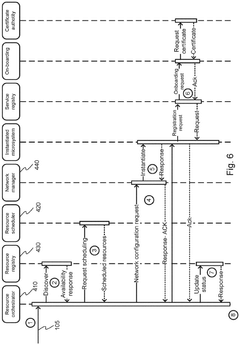
Technologies for a unified test and debug architecture
PatentWO2024205614A1
Innovation
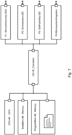
- A unified test and debug architecture is implemented using an external hardware debug interface that is interface-agnostic, employing Universal Chiplet Interconnect Express (UCIe) packets for debug messages, allowing for seamless communication and interoperability between chiplets, and enabling testing at various stages from sort stage to infield debugging.

Chiplet arrangement
PatentPendingEP4451135A1
Innovation
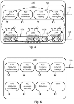
- A chiplet arrangement with a control plane that orchestrates microsystems and microservices, allowing for dynamic instantiation based on hardware resource availability and utilization, featuring a resource orchestrator, network manager, and resource scheduler to optimize resource utilization, scalability, and power management.
Supply Chain Dynamics
The supply chain dynamics in chiplet manufacturing are undergoing significant transformations as the industry embraces this innovative approach to semiconductor design and production. Chiplets, which are smaller, modular components integrated into a larger chip package, are reshaping traditional supply chain models and introducing new complexities.
One of the key trends in chiplet manufacturing supply chains is the increased emphasis on collaboration and partnerships. As chiplets often involve integrating components from multiple suppliers, manufacturers are forming strategic alliances to ensure seamless integration and compatibility. This shift towards a more collaborative ecosystem is fostering innovation and enabling the creation of more advanced and specialized chip designs.
The adoption of chiplets is also driving changes in inventory management and production planning. With the ability to mix and match different chiplets, manufacturers can potentially reduce inventory costs and improve flexibility in meeting diverse customer demands. However, this also introduces challenges in coordinating the production and delivery of various chiplet components from different suppliers.
Standardization efforts are playing a crucial role in shaping supply chain dynamics. Industry consortia and organizations are working towards establishing common interfaces and protocols for chiplet integration. These standards are essential for ensuring interoperability between chiplets from different vendors and streamlining the supply chain processes.
The geographical distribution of chiplet manufacturing is evolving, with a trend towards regionalization. As countries and regions seek to strengthen their semiconductor capabilities, we are seeing the emergence of localized chiplet ecosystems. This shift is partly driven by geopolitical factors and the desire to reduce dependence on specific regions for critical components.
Quality control and testing processes are becoming more complex in the chiplet supply chain. With multiple components from various sources being integrated into a single package, ensuring consistent quality and performance across all elements is crucial. This is leading to the development of new testing methodologies and quality assurance protocols specific to chiplet manufacturing.
The chiplet approach is also influencing logistics and transportation within the supply chain. As chiplets are smaller and more modular, there may be opportunities for more efficient shipping and handling. However, the increased number of components and suppliers involved in a single chip package can also lead to more complex logistics networks.
In conclusion, the supply chain dynamics in chiplet manufacturing are characterized by increased collaboration, flexibility, and complexity. As this technology continues to evolve, we can expect further innovations in supply chain management to address the unique challenges and opportunities presented by chiplet-based semiconductor production.
Chiplet Standards
Chiplet standards play a crucial role in the emerging trends of chiplet manufacturing techniques. As the semiconductor industry moves towards disaggregated chip designs, the need for standardization has become increasingly apparent. These standards aim to ensure interoperability, reliability, and consistency across different chiplet designs and manufacturers.
One of the most prominent chiplet standards is the Universal Chiplet Interconnect Express (UCIe). Developed by a consortium of industry leaders, UCIe provides a standardized die-to-die interconnect protocol that enables seamless integration of chiplets from different vendors. This standard addresses key aspects such as physical layer specifications, protocol layer definitions, and power management requirements.
Another significant standard in the chiplet ecosystem is the Advanced Interface Bus (AIB). AIB, developed by Intel, offers a high-bandwidth, low-latency interface for chiplet-to-chiplet communication. It has been adopted by several manufacturers and is particularly well-suited for high-performance computing applications.
The Open Compute Project (OCP) has also contributed to chiplet standardization efforts through its Open Domain-Specific Architecture (ODSA) subproject. ODSA aims to create an open chiplet ecosystem by defining standards for chiplet interfaces, packaging, and testing methodologies.
Standardization efforts extend beyond interconnects to include packaging technologies. The Joint Electron Device Engineering Council (JEDEC) has been working on standards for advanced packaging technologies that are critical for chiplet integration, such as 2.5D and 3D packaging.
As chiplet manufacturing techniques continue to evolve, new standards are emerging to address specific challenges. For instance, the Bunch of Wires (BoW) interface standard, developed by the ODSA, provides a simpler and more cost-effective alternative to high-end interfaces for certain applications.
The adoption of these standards is driving innovation in chiplet design and manufacturing. They enable designers to mix and match chiplets from different vendors, fostering a more diverse and competitive ecosystem. This modular approach allows for greater flexibility in chip design, potentially reducing development costs and time-to-market for new products.
However, challenges remain in the standardization process. Balancing the need for interoperability with the desire for proprietary innovations is an ongoing concern. Additionally, ensuring backward compatibility while accommodating future technological advancements requires careful consideration in standard development.
As chiplet manufacturing techniques continue to advance, the evolution of these standards will play a pivotal role in shaping the future of semiconductor design and production. The industry's commitment to open standards and collaborative development will be crucial in realizing the full potential of chiplet-based architectures.
Unlock deeper insights with Patsnap Eureka Quick Research — get a full tech report to explore trends and direct your research. Try now!
Generate Your Research Report Instantly with AI Agent
Supercharge your innovation with Patsnap Eureka AI Agent Platform!