

Chiplet-Based Solutions Driving Expansion in High-Tech Developments
JUL 16, 20259 MIN READ
Generate Your Research Report Instantly with AI Agent
Patsnap Eureka helps you evaluate technical feasibility & market potential.
Chiplet Technology Evolution and Objectives
Chiplet technology has emerged as a revolutionary approach in the semiconductor industry, addressing the challenges of traditional monolithic chip designs. The evolution of chiplets can be traced back to the early 2010s when the limitations of Moore's Law became increasingly apparent. As transistor scaling slowed down, chiplets offered a new paradigm for continuing performance improvements and cost reductions in integrated circuits.
The primary objective of chiplet technology is to overcome the limitations of monolithic chip designs by disaggregating complex systems-on-chip (SoCs) into smaller, more manageable dies. These smaller dies, or chiplets, can be manufactured using different process nodes and then integrated onto a single package. This approach allows for greater flexibility in design, improved yield, and the ability to mix and match different technologies within a single package.
The evolution of chiplet technology has been marked by several key milestones. In 2015, AMD introduced its Infinity Fabric interconnect, which laid the groundwork for their chiplet-based processors. Intel followed suit with its EMIB (Embedded Multi-die Interconnect Bridge) technology in 2017, enabling high-bandwidth connections between chiplets. TSMC's CoWoS (Chip on Wafer on Substrate) and InFO (Integrated Fan-Out) packaging technologies have also played crucial roles in advancing chiplet integration.
As the technology progressed, industry standards began to emerge. The development of the Universal Chiplet Interconnect Express (UCIe) standard in 2022 marked a significant step towards interoperability between chiplets from different manufacturers. This standardization is expected to accelerate the adoption of chiplet-based solutions across the industry.
The objectives of chiplet technology extend beyond merely overcoming the limitations of Moore's Law. They include enabling more customizable and scalable designs, reducing time-to-market for new products, and improving overall system performance and power efficiency. Chiplets also aim to address the increasing costs associated with advanced node manufacturing by allowing companies to mix older, more cost-effective nodes with cutting-edge technology where necessary.
Looking forward, the goals of chiplet technology include further miniaturization of interconnects, improved thermal management in multi-die packages, and the development of more sophisticated design and verification tools. There is also a push towards heterogeneous integration, combining not just different process nodes but also different types of components such as CPUs, GPUs, memory, and specialized accelerators within a single package.
Market Demand for Chiplet Solutions
The market demand for chiplet solutions has been experiencing significant growth in recent years, driven by the increasing complexity and performance requirements of modern computing systems. As traditional monolithic chip designs approach their physical limits, chiplet-based architectures have emerged as a promising alternative to meet the escalating demands of various high-tech industries.
In the data center and cloud computing sector, the need for more powerful and energy-efficient processors has led to a surge in demand for chiplet solutions. These modular designs allow for the integration of specialized components, such as high-performance CPU cores, GPU units, and AI accelerators, on a single package. This approach enables cloud service providers to offer tailored computing solutions that can handle diverse workloads more efficiently, resulting in improved performance and reduced operational costs.
The telecommunications industry, particularly with the rollout of 5G networks, has also shown a strong interest in chiplet-based solutions. The modular nature of chiplets allows for the development of flexible and scalable network infrastructure components that can adapt to the evolving requirements of 5G and future wireless technologies. This demand is further amplified by the need for edge computing capabilities, where chiplet designs can offer optimized performance in compact form factors.
In the consumer electronics market, chiplet solutions are gaining traction in high-end smartphones, tablets, and laptops. Manufacturers are leveraging chiplet technology to create more powerful and energy-efficient devices while maintaining slim profiles and extended battery life. The ability to mix and match different functional blocks allows for greater product differentiation and faster time-to-market, which is crucial in the highly competitive consumer electronics landscape.
The automotive industry is another sector driving the demand for chiplet solutions, particularly in the development of advanced driver assistance systems (ADAS) and autonomous vehicles. These applications require high-performance, low-latency computing capabilities that can be efficiently delivered through chiplet-based designs. The modular approach also allows for easier integration of specialized AI and sensor processing units, which are essential for the complex decision-making processes in autonomous driving.
Furthermore, the industrial and IoT sectors are showing increased interest in chiplet solutions for edge computing applications. The ability to create customized, high-performance computing modules that can operate in challenging environments makes chiplets an attractive option for industrial automation, smart manufacturing, and large-scale IoT deployments.
As the demand for more powerful and specialized computing solutions continues to grow across various industries, the market for chiplet-based solutions is expected to expand significantly. This trend is likely to drive further innovation in chiplet design, manufacturing processes, and integration technologies, ultimately shaping the future of high-tech developments across multiple sectors.
Chiplet Challenges and Limitations
Despite the promising potential of chiplet technology, several challenges and limitations need to be addressed for its widespread adoption and success in high-tech developments. One of the primary concerns is the complexity of integration. Chiplets require sophisticated packaging techniques and interconnect technologies to function as a cohesive unit. This integration process can be intricate and costly, potentially offsetting some of the cost advantages that chiplets offer.
Another significant challenge lies in the realm of thermal management. As chiplets allow for higher component density, managing heat dissipation becomes increasingly difficult. The compact nature of chiplet-based designs can lead to hotspots and thermal bottlenecks, potentially impacting performance and reliability. Innovative cooling solutions and thermal design considerations are crucial to overcome this limitation.
Standardization remains a key hurdle in the chiplet ecosystem. The lack of universal standards for chiplet interfaces and protocols can hinder interoperability between chiplets from different manufacturers. This fragmentation in the industry could slow down adoption and limit the potential for mix-and-match flexibility that chiplets promise.
Performance optimization across chiplets presents another challenge. Ensuring seamless communication and synchronization between different chiplets is critical for maintaining overall system performance. Latency issues and bandwidth limitations in inter-chiplet connections can potentially impact the efficiency of chiplet-based solutions compared to monolithic designs.
The testing and validation of chiplet-based systems introduce new complexities. Traditional testing methods may not be sufficient for thoroughly evaluating the performance and reliability of interconnected chiplets. Developing comprehensive testing strategies that can assess both individual chiplets and their integrated performance is essential.
Supply chain management becomes more intricate with chiplet technology. Coordinating the production and assembly of multiple chiplets from potentially different suppliers adds layers of complexity to the manufacturing process. Ensuring consistent quality and timely delivery of all components is crucial for successful chiplet-based product development.
Lastly, the intellectual property (IP) landscape surrounding chiplet technology is still evolving. Issues related to IP ownership, licensing, and protection in a multi-vendor chiplet ecosystem need to be carefully navigated. Clear frameworks for IP management and collaboration are necessary to foster innovation and cooperation in the chiplet space.
Current Chiplet Integration Approaches
01 Chiplet integration for advanced computing systems
Chiplet-based solutions are expanding to enable more powerful and efficient computing systems. This approach involves integrating multiple smaller chiplets onto a single package, allowing for improved performance, scalability, and cost-effectiveness in various applications such as high-performance computing, artificial intelligence, and data centers.- Chiplet integration for improved performance: Chiplet-based solutions allow for the integration of multiple specialized chips on a single package, enabling improved performance and efficiency. This approach allows for mixing and matching of different process nodes and technologies, optimizing cost and performance for specific applications.
- Interconnect technologies for chiplets: Advanced interconnect technologies are crucial for chiplet-based designs, enabling high-bandwidth, low-latency communication between different chiplets. These technologies include advanced packaging techniques, through-silicon vias (TSVs), and high-speed SerDes interfaces.
- Thermal management in chiplet designs: Effective thermal management is essential in chiplet-based solutions due to the high power density of tightly integrated components. Innovative cooling solutions and thermal design considerations are implemented to ensure optimal performance and reliability of chiplet-based systems.
- Chiplet-based AI and machine learning acceleration: Chiplet architectures are being leveraged to create specialized AI and machine learning accelerators. By combining different types of processing elements and memory subsystems as chiplets, highly efficient and scalable AI solutions can be developed.
- Standardization and interoperability in chiplet ecosystems: Efforts are being made to standardize chiplet interfaces and protocols to enable interoperability between chiplets from different vendors. This standardization aims to create a more diverse and competitive chiplet ecosystem, allowing for greater flexibility in system design and reducing time-to-market.
02 Interconnect technologies for chiplet-based designs
Advanced interconnect technologies are being developed to facilitate communication between chiplets and improve overall system performance. These include high-bandwidth interfaces, through-silicon vias (TSVs), and novel packaging solutions that enable seamless integration of heterogeneous chiplets from different process nodes or manufacturers.Expand Specific Solutions03 Chiplet-based solutions for memory and storage
The expansion of chiplet-based solutions is extending to memory and storage systems, enabling higher capacity, improved bandwidth, and reduced power consumption. This approach allows for the integration of different memory technologies and storage components within a single package, optimizing performance for specific applications.Expand Specific Solutions04 Thermal management and power efficiency in chiplet designs
As chiplet-based solutions expand, innovative thermal management techniques and power efficiency strategies are being developed. These include advanced cooling solutions, power gating mechanisms, and intelligent power distribution systems to optimize performance while managing heat dissipation and energy consumption in complex multi-chiplet designs.Expand Specific Solutions05 Chiplet-based solutions for edge computing and IoT devices
The expansion of chiplet-based solutions is reaching edge computing and Internet of Things (IoT) devices, enabling more powerful and efficient processing capabilities in compact form factors. This approach allows for the integration of specialized chiplets for tasks such as AI inference, security, and connectivity, tailored to the specific requirements of edge and IoT applications.Expand Specific Solutions
Key Players in Chiplet Industry
The chiplet-based solutions market is in a growth phase, driven by increasing demand for high-performance computing and AI applications. The market size is expanding rapidly, with major players like Intel, AMD, and Micron Technology investing heavily in chiplet technology. The competitive landscape is characterized by a mix of established semiconductor giants and innovative startups like AvicenaTech and Primemas. Technological maturity varies, with some companies like Intel and AMD already commercializing chiplet-based products, while others are still in research and development stages. Chinese companies and research institutions, such as Zhejiang Lab and Beijing University of Technology, are also making significant strides in chiplet technology, indicating a global race for innovation in this field.
Micron Technology, Inc.
Technical Solution: Micron's approach to chiplet-based solutions focuses on advanced memory technologies and their integration with compute elements. Their Hybrid Memory Cube (HMC) technology, while not strictly a chiplet design, laid the groundwork for 3D-stacked memory solutions[10]. More recently, Micron has been developing High Bandwidth Memory (HBM) products, which are crucial components in many chiplet-based designs. Their HBM2E memory, offering bandwidth up to 460 GB/s per stack, is designed to be integrated with high-performance processors and AI accelerators[11]. Micron is also exploring innovative packaging technologies, including their multi-chip package (MCP) solutions, which combine different types of memory (e.g., LPDDR and NAND) in a single package, aligning with the chiplet philosophy of modular integration[12].
Strengths: Advanced memory technologies crucial for chiplet integration, expertise in 3D stacking and high-bandwidth solutions. Weaknesses: Limited direct involvement in compute chiplet design, reliance on partnerships for full system integration.
Intel Corp.
Technical Solution: Intel's chiplet-based solution, Foveros 3D packaging technology, enables the stacking of diverse silicon dies vertically[1]. This approach allows for the integration of high-performance compute tiles with low-power base dies, optimizing both performance and power efficiency. Intel's Ponte Vecchio GPU, built on this technology, incorporates over 100 billion transistors across 47 tiles[2], demonstrating the scalability and flexibility of their chiplet approach. The company has also introduced their next-generation Foveros Direct technology, which promises to reduce the interconnect pitch to sub-10 microns, further enhancing die-to-die connections[3].
Strengths: Advanced 3D packaging technology, proven scalability, and flexibility in chip design. Weaknesses: Potential thermal management challenges in densely packed 3D structures and higher manufacturing complexity.
Core Chiplet Innovations
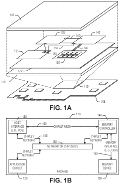
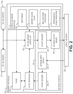
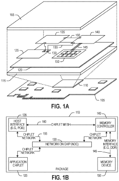
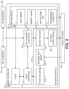
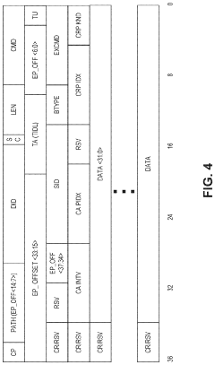
Communicating a programmable atomic operator to a memory controller
PatentPendingUS20230244416A1
Innovation
- A packet-based request and response technique is introduced to specify and invoke programmable atomic operators (PAOs) within a chiplet system, allowing for flexible and efficient invocation of PAOs by routing request packets through a packet-based network and decoding them to invoke the appropriate PAO, with responses transmitted back to the requesting process.
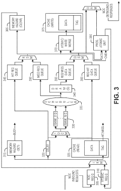
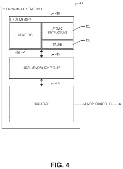
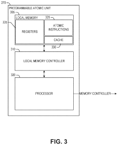
Detecting infinite loops in a programmable atomic transaction
PatentActiveUS11989556B2
Innovation
- Implementing a programmable atomic unit with an instruction counter to track the execution of instructions and set an instruction execution limit, allowing for the termination of transactions that exceed this limit, thereby preventing infinite loops and ensuring resource availability.
Chiplet Ecosystem Development
The chiplet ecosystem has been rapidly evolving, driven by the increasing demand for high-performance computing solutions and the limitations of traditional monolithic chip designs. This ecosystem encompasses a wide range of stakeholders, including semiconductor manufacturers, packaging companies, electronic design automation (EDA) tool providers, and system integrators.
At the core of the chiplet ecosystem are the chiplet manufacturers, who produce specialized silicon dies that can be integrated into larger systems. These manufacturers are developing diverse chiplet portfolios, ranging from processing units and memory modules to specialized accelerators for AI and machine learning applications. The ecosystem also includes packaging companies that are advancing technologies such as 2.5D and 3D integration, enabling the efficient interconnection of multiple chiplets.
Interoperability standards play a crucial role in the chiplet ecosystem's development. Organizations like the Open Compute Project (OCP) and CHIPS Alliance are working to establish common interfaces and protocols, such as the Universal Chiplet Interconnect Express (UCIe), to ensure seamless integration between chiplets from different vendors. These standards are essential for fostering a more open and competitive marketplace.
EDA tool providers are adapting their software suites to support chiplet-based design workflows. These tools are evolving to handle the complexities of multi-die systems, including thermal management, power distribution, and signal integrity across chiplet interfaces. Additionally, the ecosystem is seeing the emergence of specialized design services and IP providers that offer pre-validated chiplet designs and integration solutions.
The chiplet ecosystem is also driving innovations in testing and validation methodologies. New approaches are being developed to ensure the reliability and performance of multi-chiplet systems, including advanced probe technologies and system-level test strategies. This aspect of the ecosystem is critical for maintaining quality standards as chiplet-based designs become more prevalent in high-stakes applications such as data centers and automotive systems.
As the ecosystem matures, we are witnessing increased collaboration between traditionally competitive companies. Joint ventures and strategic partnerships are forming to leverage complementary strengths and accelerate the adoption of chiplet technologies. This collaborative approach is essential for addressing the complex challenges associated with chiplet integration and for realizing the full potential of disaggregated chip designs.
Chiplet Standardization Efforts
Chiplet standardization efforts have become a crucial aspect of the semiconductor industry's evolution towards more modular and scalable chip designs. These initiatives aim to establish common interfaces, protocols, and design methodologies that enable seamless integration of chiplets from different vendors. The primary goal is to create an ecosystem where chiplets can be mixed and matched like building blocks, fostering innovation and reducing development costs.
One of the most prominent standardization efforts is the Universal Chiplet Interconnect Express (UCIe) consortium. Launched in 2022, UCIe brings together industry giants like Intel, AMD, Arm, TSMC, and Samsung to develop an open specification for die-to-die interconnects. The UCIe 1.0 specification, released in March 2022, defines the physical and protocol layers for chiplet-to-chiplet communication, enabling high-bandwidth, low-latency connections between chiplets.
Another significant initiative is the Open Compute Project's (OCP) Chiplet Design Exchange (CDX) working group. CDX focuses on creating standardized chiplet models and design methodologies to facilitate the exchange of chiplet designs between different companies. This effort aims to reduce the complexity of integrating chiplets from multiple sources and accelerate time-to-market for chiplet-based products.
The CHIPS Alliance, an open-source hardware initiative, is also contributing to chiplet standardization through its Advanced Interface Bus (AIB) specification. AIB provides a standardized die-to-die interface that enables high-speed communication between chiplets, supporting both 2D and 3D integration technologies.
In addition to these industry-led efforts, government agencies and research institutions are also playing a role in chiplet standardization. For instance, the Defense Advanced Research Projects Agency (DARPA) has launched the Common Heterogeneous Integration and IP Reuse Strategies (CHIPS) program, which aims to develop standards and tools for modular chip design and integration.
As chiplet standardization efforts progress, they face several challenges. These include ensuring backward compatibility with existing chip designs, addressing security concerns related to multi-vendor chiplet integration, and balancing the need for standardization with the desire for proprietary innovations. Despite these challenges, the industry recognizes the importance of standardization in unlocking the full potential of chiplet-based solutions and driving expansion in high-tech developments.
Unlock deeper insights with Patsnap Eureka Quick Research — get a full tech report to explore trends and direct your research. Try now!
Generate Your Research Report Instantly with AI Agent
Supercharge your innovation with Patsnap Eureka AI Agent Platform!