How Chiplets Enhance Connectivity in Broadening Data Systems?
JUL 16, 20259 MIN READ
Generate Your Research Report Instantly with AI Agent
Patsnap Eureka helps you evaluate technical feasibility & market potential.
Chiplet Tech Evolution
The evolution of chiplet technology represents a paradigm shift in the semiconductor industry, moving from monolithic chip designs to modular, multi-die architectures. This transition has been driven by the increasing demand for higher performance, lower power consumption, and improved scalability in data systems.
In the early 2010s, the concept of chiplets began to gain traction as a solution to the limitations of traditional monolithic chip designs. The initial focus was on disaggregating large, complex chips into smaller, more manageable components. This approach allowed for better yield management and the ability to mix and match different process nodes within a single package.
As the technology progressed, the emphasis shifted towards enhancing connectivity between chiplets. The development of high-bandwidth, low-latency interconnects became crucial for realizing the full potential of chiplet-based designs. Advanced packaging technologies, such as 2.5D and 3D integration, emerged as key enablers for chiplet connectivity.
The mid-2010s saw the introduction of silicon interposers, which provided a platform for integrating multiple chiplets with high-speed interconnects. This technology allowed for wider data buses and shorter signal paths between chiplets, significantly improving overall system performance.
In recent years, the focus has shifted towards more advanced interconnect technologies, such as die-to-die bridges and through-silicon vias (TSVs). These innovations have further reduced latency and increased bandwidth between chiplets, enabling more complex and efficient multi-die architectures.
The latest developments in chiplet technology have centered on standardization efforts, such as the Universal Chiplet Interconnect Express (UCIe) specification. This initiative aims to create a common interface for chiplets from different vendors, promoting interoperability and accelerating adoption across the industry.
Looking ahead, the evolution of chiplet technology is expected to continue with advancements in packaging materials, interconnect technologies, and design methodologies. Emerging technologies, such as photonic interconnects and advanced cooling solutions, are poised to further enhance the connectivity and performance of chiplet-based systems.
As data systems continue to expand and diversify, chiplet technology is playing an increasingly critical role in addressing the challenges of scalability, performance, and power efficiency. The modular nature of chiplets allows for more flexible and customizable system designs, enabling the creation of tailored solutions for a wide range of applications, from edge computing to high-performance data centers.
Data System Market Trends
The data system market is experiencing rapid growth and transformation, driven by the increasing volume, velocity, and variety of data generated across various industries. This surge in data production and consumption is fueling demand for more sophisticated and efficient data management solutions. Cloud computing and edge computing are playing pivotal roles in shaping the market landscape, with organizations increasingly adopting hybrid and multi-cloud strategies to optimize their data infrastructure.
The rise of artificial intelligence and machine learning applications is a significant factor influencing market trends. These technologies require robust data systems capable of handling complex computations and large-scale data processing. As a result, there is a growing demand for high-performance computing solutions and specialized hardware accelerators designed to support AI workloads.
Data analytics and business intelligence tools are becoming increasingly important as organizations seek to extract valuable insights from their data assets. This trend is driving the development of more advanced analytics platforms and visualization tools, capable of processing and presenting complex data sets in real-time.
The Internet of Things (IoT) is another major force shaping the data system market. The proliferation of connected devices is generating vast amounts of data at the edge, necessitating the development of edge computing solutions and more efficient data transfer mechanisms between edge devices and centralized data centers.
Data security and privacy concerns are also influencing market trends, with organizations placing greater emphasis on data protection and compliance with regulatory requirements. This has led to increased investment in data encryption, access control, and data governance solutions.
The shift towards software-defined infrastructure and disaggregated hardware architectures is gaining momentum in the data system market. This approach allows for greater flexibility and scalability in data center design, enabling organizations to adapt more quickly to changing business requirements and technological advancements.
As data volumes continue to grow exponentially, there is a rising demand for more efficient and scalable storage solutions. This has led to innovations in storage technologies, including advancements in solid-state drives, non-volatile memory express (NVMe) protocols, and software-defined storage systems.
Chiplet Connectivity Challenges
As chiplets continue to revolutionize the semiconductor industry, they bring forth a new set of connectivity challenges that must be addressed to fully realize their potential in broadening data systems. One of the primary hurdles is the need for high-bandwidth, low-latency interconnects between chiplets. Traditional package-level interconnects often fall short in meeting the demanding requirements of chiplet-based designs, necessitating innovative solutions.
The integration of heterogeneous chiplets poses another significant challenge. Different chiplets may be manufactured using various process nodes, have distinct power requirements, or operate at different frequencies. Ensuring seamless communication and synchronization between these diverse components requires sophisticated interface protocols and signal integrity management.
Thermal management emerges as a critical concern in chiplet-based systems. The dense packaging of multiple chiplets can lead to localized hotspots and overall thermal challenges that may impact system performance and reliability. Developing effective cooling solutions and thermal-aware designs becomes paramount in addressing this issue.
Power delivery and distribution across chiplets present another layer of complexity. As chiplets are often smaller and more numerous than traditional monolithic dies, ensuring efficient and stable power delivery to each component becomes increasingly challenging. This necessitates advanced power distribution networks and potentially new packaging technologies.
Signal integrity and electromagnetic interference (EMI) management are crucial aspects of chiplet connectivity. The close proximity of multiple high-speed interconnects can lead to crosstalk and signal degradation. Mitigating these effects requires careful design considerations, advanced shielding techniques, and potentially new materials for package substrates.
Standardization of chiplet interfaces and protocols is an ongoing challenge in the industry. While initiatives like Universal Chiplet Interconnect Express (UCIe) are making strides, the lack of widespread, universally adopted standards can hinder interoperability and limit the potential for mix-and-match chiplet designs across different vendors.
Testing and validation of chiplet-based systems introduce new complexities. Traditional testing methodologies may not be sufficient for thoroughly evaluating the intricate interactions between multiple chiplets. Developing comprehensive test strategies that can assess both individual chiplet functionality and system-level performance is essential.
Lastly, the challenge of yield management in chiplet production cannot be overlooked. While chiplets offer the potential for improved overall yield compared to large monolithic dies, they introduce new considerations in terms of known-good-die testing and the logistics of assembling multiple chiplets into a single package.
Current Chiplet Solutions
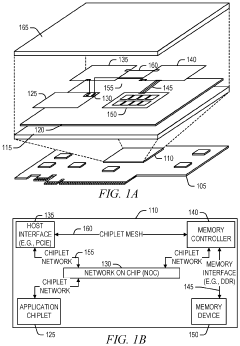
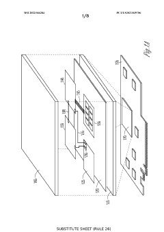
01 Interconnect technologies for chiplet integration
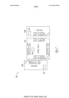
Various interconnect technologies are employed to enable efficient communication between chiplets. These may include advanced packaging techniques, high-speed interfaces, and novel interconnect architectures designed to optimize data transfer between different chiplets within a multi-chip module.- Interconnect technologies for chiplet integration: Advanced interconnect technologies are crucial for efficient chiplet integration. These include high-bandwidth interfaces, through-silicon vias (TSVs), and interposers that enable high-speed communication between chiplets. Such technologies facilitate the creation of complex multi-chip modules with improved performance and reduced power consumption.
- Packaging solutions for chiplet connectivity: Innovative packaging solutions play a vital role in chiplet connectivity. These include 2.5D and 3D packaging techniques, advanced substrate technologies, and novel die-to-die bonding methods. Such packaging approaches enable closer integration of chiplets, reducing signal path lengths and improving overall system performance.
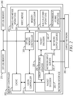
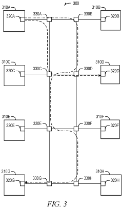
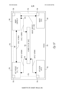
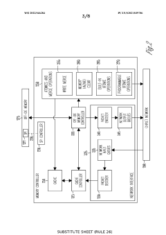
- Network-on-Chip (NoC) architectures for chiplet communication: Network-on-Chip architectures are being developed to facilitate efficient communication between chiplets. These architectures provide scalable and flexible interconnect solutions, allowing for optimized data transfer between multiple chiplets in complex system-on-chip designs.
- Power management and distribution for chiplet systems: Effective power management and distribution strategies are essential for chiplet-based systems. This includes techniques for voltage regulation, power gating, and thermal management across multiple chiplets. Such approaches ensure optimal performance while maintaining power efficiency in heterogeneous chiplet configurations.
- Standardization and interoperability in chiplet connectivity: Efforts are being made to establish standards and ensure interoperability in chiplet connectivity. This includes the development of common interfaces, protocols, and design methodologies that allow chiplets from different vendors to work together seamlessly. Standardization facilitates the creation of a diverse ecosystem of chiplet-based solutions.
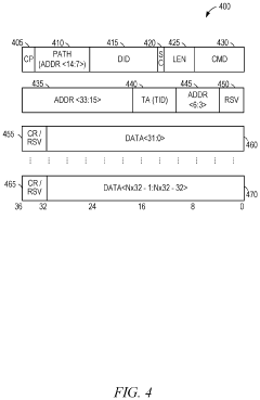
02 Chiplet-to-chiplet communication protocols
Specialized communication protocols are developed to facilitate seamless data exchange between chiplets. These protocols are designed to handle high-bandwidth, low-latency communications while addressing challenges such as power efficiency and signal integrity in multi-chiplet systems.Expand Specific Solutions03 3D integration and stacking for chiplet connectivity
Three-dimensional integration and stacking techniques are utilized to enhance chiplet connectivity. These approaches involve vertically stacking chiplets and implementing through-silicon vias (TSVs) or other advanced interconnect methods to achieve higher bandwidth and reduced latency between chiplets.Expand Specific Solutions04 Network-on-Chip (NoC) architectures for chiplets
Network-on-Chip architectures are adapted for chiplet-based systems to provide scalable and efficient communication infrastructure. These NoC designs are optimized to handle the unique requirements of inter-chiplet connectivity, including routing, arbitration, and quality of service considerations.Expand Specific Solutions05 Packaging and thermal management for chiplet connectivity
Advanced packaging solutions and thermal management techniques are developed to support high-performance chiplet connectivity. These innovations address challenges related to power delivery, heat dissipation, and signal integrity in densely interconnected chiplet-based systems.Expand Specific Solutions
Key Chiplet Manufacturers
The chiplet technology market is in its early growth stage, with increasing adoption across the semiconductor industry. The market size is expanding rapidly, driven by the need for more efficient and scalable chip designs. Technologically, chiplets are maturing, with major players like Intel, AMD, and TSMC making significant advancements. Companies such as Micron Technology, Intel, and Xilinx are at the forefront of chiplet innovation, developing advanced interconnect technologies and packaging solutions. Other key players like Cisco, ZTE, and Huawei are also investing in chiplet-based designs for their networking and communication products. As the technology evolves, we can expect increased collaboration and standardization efforts among industry leaders to further enhance chiplet connectivity and integration in broadening data systems.
Intel Corp.
Technical Solution: Intel's approach to chiplet technology focuses on their Advanced Interface Bus (AIB) and Embedded Multi-die Interconnect Bridge (EMIB) technologies. AIB is a die-to-die interconnect that allows for high-bandwidth, low-power communication between chiplets[1]. EMIB technology enables the integration of multiple silicon dies onto a single package substrate, reducing the need for expensive silicon interposers[2]. Intel's Foveros 3D packaging technology further enhances connectivity by allowing vertical stacking of chiplets, enabling higher bandwidth and lower latency between components[3]. These technologies collectively allow Intel to mix and match different process nodes and IP blocks, optimizing performance, power, and cost for various data system applications[4].
Strengths: High bandwidth, low latency interconnects; flexibility in chip design; cost-effective integration of heterogeneous technologies. Weaknesses: Complexity in design and manufacturing; thermal management challenges in 3D stacked configurations.
Xilinx, Inc.
Technical Solution: Xilinx, now part of AMD, has developed the Adaptive Compute Acceleration Platform (ACAP) that leverages chiplet technology. Their Versal ACAP architecture combines programmable logic, DSP engines, and ARM cores on a single chip, using a Network on Chip (NoC) for high-speed communication between components[5]. The Versal Premium series incorporates chiplets for specific functions like 600G ethernet and PCIe Gen5, enhancing connectivity for data-intensive applications[6]. Xilinx's approach allows for customizable, high-performance computing solutions that can be tailored to specific data system requirements, from edge computing to data centers[7].
Strengths: Highly customizable and adaptable architecture; integration of diverse computing elements; excellent for specialized, high-performance applications. Weaknesses: Complexity in programming and optimization; potentially higher cost for some applications compared to fixed-function alternatives.
Chiplet Interconnect Innovations
Network credit return mechanisms
PatentActiveUS11966345B2
Innovation
- Implementing a method where only one flit per transfer cycle includes credit return data, using a wide bus to select from multiple credit return options, and employing bitwise-OR operations to combine credit return data, reducing the need for additional circuitry and minimizing delays in the critical path.
Method for configuring multiple input-output channels
PatentWO2022046284A1
Innovation
- The implementation of a Chiplet Protocol Interface (CPI) network with Advanced Interface Bus (AIB) channels and credit-based flow control, allowing for flexible virtual channel mapping and minimizing latency and energy consumption through packetized protocols and serialization-deserialization (SERDES) hardware, while enabling efficient inter-chiplet communication.
Chiplet Standardization Efforts
Chiplet standardization efforts have become increasingly crucial in the semiconductor industry as the adoption of chiplet-based designs continues to grow. These initiatives aim to establish common interfaces, protocols, and design methodologies to facilitate interoperability and integration of chiplets from different vendors. The development of industry-wide standards is essential for promoting innovation, reducing costs, and accelerating time-to-market for chiplet-based products.
One of the most prominent standardization efforts is the Universal Chiplet Interconnect Express (UCIe) consortium, which includes major players such as Intel, AMD, Arm, and TSMC. UCIe focuses on creating a standardized die-to-die interconnect that enables seamless integration of chiplets from various manufacturers. The consortium has released specifications for physical layer, protocol layer, and software stack, providing a comprehensive framework for chiplet integration.
Another significant initiative is the Open Compute Project's (OCP) Chiplet Design Exchange (CDX) working group. CDX aims to develop open standards for chiplet-based designs, focusing on areas such as thermal management, power delivery, and signal integrity. By addressing these critical aspects, CDX seeks to improve the overall performance and reliability of chiplet-based systems.
The CHIPS Alliance, an open-source hardware initiative, is also contributing to chiplet standardization efforts. Their work includes developing open-source tools and methodologies for chiplet design and integration, which can help reduce barriers to entry for smaller companies and accelerate innovation in the field.
Standardization efforts extend beyond interconnects and design methodologies to include packaging technologies. The Joint Electron Device Engineering Council (JEDEC) has been working on standards for advanced packaging technologies, including those used in chiplet-based designs. These standards address issues such as thermal management, reliability testing, and mechanical specifications for multi-chip packages.
The success of these standardization efforts is critical for the widespread adoption of chiplet technology. By establishing common interfaces and protocols, these initiatives enable a more diverse and competitive ecosystem of chiplet suppliers. This, in turn, can lead to increased innovation, reduced costs, and improved performance in data systems and other applications that rely on advanced semiconductor technologies.
As chiplet technology continues to evolve, ongoing collaboration between industry leaders, research institutions, and standards organizations will be essential to ensure that standardization efforts keep pace with technological advancements. This collaborative approach will be crucial in addressing emerging challenges and opportunities in chiplet-based designs, ultimately driving the continued growth and innovation in the semiconductor industry.
Chiplet Economic Impact
The economic impact of chiplets on the semiconductor industry and broader technology ecosystem is profound and multifaceted. By enabling the disaggregation of complex System-on-Chip (SoC) designs into smaller, more manageable components, chiplets are revolutionizing the economics of chip production and system integration.
One of the most significant economic benefits of chiplets is the potential for cost reduction in semiconductor manufacturing. Traditional monolithic chip designs become increasingly expensive to produce as they grow in size and complexity. Chiplets allow manufacturers to break down these large designs into smaller, more yield-friendly components. This approach can significantly improve production yields, as defects in one chiplet do not necessarily render the entire system unusable. The result is a more cost-effective manufacturing process, potentially leading to lower prices for end consumers and improved profit margins for manufacturers.
Chiplets also offer enhanced flexibility in product development and time-to-market advantages. Companies can mix and match different chiplets to create a wide range of products without designing entirely new chips for each application. This modular approach reduces development costs and accelerates product cycles, allowing companies to respond more quickly to market demands and technological advancements.
The chiplet ecosystem is fostering increased collaboration and specialization within the semiconductor industry. Companies can focus on developing specific chiplets that align with their core competencies, rather than attempting to master every aspect of chip design. This specialization can lead to more innovative and optimized components, as well as create new business models and partnership opportunities within the industry.
Furthermore, chiplets are enabling smaller companies and startups to enter the market more easily. The reduced barriers to entry in terms of design and manufacturing costs allow for greater competition and innovation in the semiconductor space. This democratization of chip design could lead to a more diverse and dynamic industry landscape, potentially accelerating technological progress and economic growth in the sector.
The adoption of chiplets is also driving investments in advanced packaging technologies and interconnect solutions. As the demand for high-performance chiplet-based systems grows, there is an increasing need for sophisticated packaging techniques to integrate these components efficiently. This trend is creating new economic opportunities in adjacent industries and spurring further innovation in materials science and manufacturing processes.
Unlock deeper insights with Patsnap Eureka Quick Research — get a full tech report to explore trends and direct your research. Try now!
Generate Your Research Report Instantly with AI Agent
Supercharge your innovation with Patsnap Eureka AI Agent Platform!