

How Chiplets Address Challenges in Emerging Computing Technologies?
JUL 16, 20258 MIN READ
Generate Your Research Report Instantly with AI Agent
Patsnap Eureka helps you evaluate technical feasibility & market potential.
Chiplet Technology Evolution and Objectives
Chiplet technology has emerged as a revolutionary approach in the semiconductor industry, addressing critical challenges in emerging computing technologies. The evolution of chiplets can be traced back to the early 2010s when traditional monolithic chip designs began to face limitations in performance scaling and manufacturing costs. As Moore's Law slowed down, chiplets offered a promising solution to continue advancing computing capabilities.
The primary objective of chiplet technology is to overcome the limitations of monolithic chip designs by disaggregating complex systems into smaller, more manageable components. This approach aims to improve yield, reduce costs, and enhance overall system performance. By allowing different functional blocks to be manufactured separately and then integrated, chiplets enable the use of optimal process nodes for each component, resulting in better performance and power efficiency.
One of the key drivers behind chiplet adoption is the increasing demand for heterogeneous computing in emerging technologies such as artificial intelligence, 5G communications, and edge computing. These applications require a diverse set of specialized processing units, which can be more efficiently implemented using chiplets. The modular nature of chiplets allows for greater flexibility in system design, enabling customization and rapid iteration of products to meet evolving market needs.
The evolution of chiplet technology has been marked by several significant milestones. In 2017, AMD introduced its Infinity Fabric interconnect, which laid the groundwork for their chiplet-based processor designs. This was followed by the launch of the EPYC server processors and Ryzen desktop CPUs, demonstrating the viability of chiplets in high-performance computing. Intel also embraced chiplets with its Foveros 3D packaging technology, introduced in 2018, which enables vertical stacking of chiplets.
As the technology progressed, industry standards began to emerge. The development of the Universal Chiplet Interconnect Express (UCIe) standard in 2022 marked a significant step towards interoperability between chiplets from different manufacturers. This standardization effort aims to create an ecosystem where chiplets can be mixed and matched, fostering innovation and competition in the semiconductor industry.
Looking ahead, the objectives of chiplet technology continue to evolve. Future goals include further miniaturization of chiplets, improved energy efficiency, and enhanced integration techniques. Research is ongoing to develop advanced packaging technologies that can support higher bandwidth and lower latency interconnects between chiplets. Additionally, there is a growing focus on developing design tools and methodologies specifically tailored for chiplet-based systems, aiming to streamline the development process and reduce time-to-market for new products.
Market Demand for Advanced Computing Solutions
The demand for advanced computing solutions has been steadily increasing across various industries, driven by the need for higher performance, improved energy efficiency, and enhanced functionality. As traditional computing technologies approach their physical limits, chiplet-based architectures have emerged as a promising solution to address these challenges.
The market for high-performance computing (HPC) and data center applications continues to grow rapidly, with organizations seeking more powerful and efficient systems to handle complex workloads such as artificial intelligence, machine learning, and big data analytics. These applications require significant computational power and memory bandwidth, pushing the boundaries of conventional monolithic chip designs.
In the consumer electronics sector, there is a growing demand for devices with advanced features and capabilities, such as smartphones, tablets, and wearables. These devices require increasingly sophisticated processors that can deliver high performance while maintaining low power consumption and compact form factors. Chiplet technology offers a potential solution by allowing manufacturers to combine different functional units optimized for specific tasks.
The automotive industry is another key driver of demand for advanced computing solutions, particularly in the development of autonomous vehicles and advanced driver assistance systems (ADAS). These applications require powerful processors capable of real-time data processing and decision-making, while also meeting strict power and thermal constraints.
Edge computing and Internet of Things (IoT) applications are also fueling the need for more efficient and flexible computing architectures. As the number of connected devices continues to grow exponentially, there is a rising demand for processors that can handle diverse workloads at the edge while minimizing power consumption and latency.
The telecommunications industry, particularly with the rollout of 5G networks, is driving demand for advanced computing solutions in network infrastructure. Base stations and other network equipment require high-performance processors capable of handling increased data throughput and complex signal processing tasks.
As organizations across various sectors seek to improve their operational efficiency and competitiveness, there is a growing interest in specialized accelerators for specific workloads, such as AI inference, video processing, and cryptography. Chiplet technology enables the integration of these specialized components alongside general-purpose processors, offering a flexible and scalable solution to meet diverse computing needs.
Current Challenges in Semiconductor Manufacturing
The semiconductor industry is facing unprecedented challenges as it approaches the physical limits of traditional Moore's Law scaling. As transistor sizes continue to shrink, manufacturers are encountering significant hurdles in maintaining performance improvements while managing power consumption and costs. One of the primary challenges is the increasing difficulty in lithography processes, particularly in extreme ultraviolet (EUV) lithography, which is essential for producing chips at 7nm and below. The complexity and cost of EUV equipment have skyrocketed, making it economically viable for only a handful of leading-edge manufacturers.
Another critical challenge is the rising power density and thermal management issues in advanced nodes. As more transistors are packed into smaller areas, heat dissipation becomes a major concern, potentially limiting clock speeds and overall chip performance. This problem is exacerbated by the increasing prevalence of dark silicon, where portions of the chip must remain inactive to prevent overheating.
Interconnect scaling has also become a significant bottleneck. As feature sizes decrease, the resistance and capacitance of on-chip wires increase, leading to higher power consumption and signal delays. This phenomenon, known as the interconnect bottleneck, is becoming a limiting factor in chip performance and efficiency.
The increasing complexity of chip designs has led to escalating development costs and longer time-to-market cycles. The need for more sophisticated design tools, verification processes, and mask sets has made it increasingly challenging for smaller players to compete in the high-end semiconductor market.
Furthermore, the industry is grappling with the challenges of quantum effects and variability at advanced nodes. As transistors approach atomic scales, quantum tunneling and other quantum phenomena become more pronounced, leading to increased leakage current and unpredictable behavior. Variability in manufacturing processes also becomes more significant, affecting yield rates and chip reliability.
Lastly, the semiconductor industry is facing geopolitical and supply chain challenges. The concentration of advanced manufacturing capabilities in a few geographic regions has raised concerns about supply chain resilience and national security implications. This has led to efforts to diversify and localize semiconductor manufacturing, adding another layer of complexity to the industry landscape.
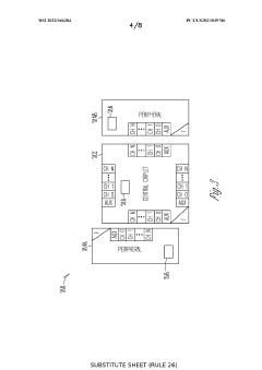
Existing Chiplet Integration Approaches
01 Chiplet integration and packaging
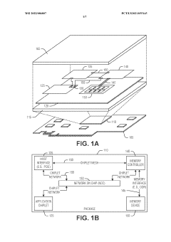
Chiplets are integrated circuit dies that can be combined in a single package to create more complex systems. This approach allows for modular design, improved yield, and cost-effective scaling of semiconductor devices. Advanced packaging technologies are used to interconnect these chiplets, enabling high-performance and power-efficient systems.- Chiplet integration and packaging: Chiplets are integrated circuit dies that can be combined to form larger, more complex systems. This approach allows for modular design and improved manufacturing yields. Advanced packaging techniques are used to interconnect these chiplets, enabling high-performance and cost-effective multi-chip solutions.
- Interconnect technologies for chiplets: Various interconnect technologies are employed to facilitate communication between chiplets. These may include advanced interposers, through-silicon vias (TSVs), and high-bandwidth interfaces. The choice of interconnect technology impacts the overall performance, power efficiency, and form factor of the chiplet-based system.
- Thermal management in chiplet designs: Effective thermal management is crucial in chiplet-based systems due to the high power density and potential for hotspots. Innovative cooling solutions, including advanced heat spreaders, liquid cooling, and thermal interface materials, are developed to maintain optimal operating temperatures and ensure reliability.
- Power distribution and management for chiplets: Efficient power distribution and management are essential for chiplet-based systems. This includes developing advanced power delivery networks, voltage regulation techniques, and power gating strategies to optimize energy consumption across multiple chiplets while maintaining performance and reliability.
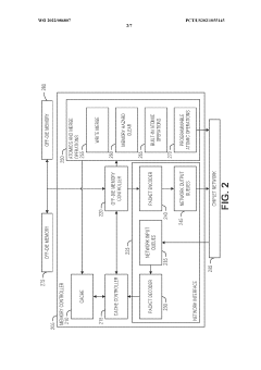
- Design and verification methodologies for chiplet-based systems: Developing robust design and verification methodologies is crucial for chiplet-based systems. This includes creating standardized interfaces, implementing system-level simulation and modeling techniques, and developing new EDA tools to handle the complexities of multi-chiplet designs and ensure overall system functionality and performance.
02 Interconnect technologies for chiplets
Various interconnect technologies are employed to connect chiplets within a package. These may include through-silicon vias (TSVs), micro-bumps, and advanced interposers. The choice of interconnect technology affects the overall performance, power consumption, and thermal characteristics of the chiplet-based system.Expand Specific Solutions03 Chiplet-based system architecture
Chiplet-based systems can be designed with different architectures to optimize performance, power efficiency, and functionality. This may involve heterogeneous integration of chiplets with different process nodes or specialized functions, such as CPUs, GPUs, memory, and I/O interfaces.Expand Specific Solutions04 Thermal management in chiplet designs
Effective thermal management is crucial in chiplet-based systems due to the high power density and potential hotspots. Advanced cooling solutions, such as integrated liquid cooling or novel heat spreader designs, are developed to maintain optimal operating temperatures and ensure reliability.Expand Specific Solutions05 Testing and yield improvement for chiplets
Specialized testing methodologies are developed for chiplet-based systems to ensure functionality and performance. These may include pre-packaging tests, known-good-die selection, and post-packaging validation. Yield improvement techniques are also employed to maximize the overall system yield and reduce manufacturing costs.Expand Specific Solutions
Key Players in Chiplet Technology Ecosystem
The chiplet technology market is in a growth phase, with increasing adoption across the computing industry. Major players like Intel, AMD, and Micron are investing heavily in chiplet-based architectures to address challenges in emerging computing technologies. The market size is expanding rapidly, driven by demand for more efficient and scalable chip designs. Technologically, chiplets are maturing but still evolving, with companies like Primemas developing specialized hub chiplets to enable modular SoC designs. While established semiconductor giants lead in production, startups and research institutions are also making significant contributions to chiplet innovation. The competitive landscape is dynamic, with both collaboration and competition between key players as the technology continues to advance.
Micron Technology, Inc.
Technical Solution: Micron's approach to chiplets focuses on memory solutions. They are developing High Bandwidth Memory (HBM) chiplets that can be integrated with processors using advanced packaging technologies. Micron's HBM3 technology offers bandwidth up to 921 GB/s, significantly enhancing performance for data-intensive applications[7]. The company is also working on Hybrid Memory Cube (HMC) technology, which stacks multiple DRAM dies vertically and includes a logic layer for intelligent memory management[8]. Micron is exploring the use of through-silicon vias (TSVs) and micro-bumps to enable high-density, high-performance memory chiplets[9].
Strengths: Expertise in memory technologies, high-bandwidth solutions, and vertical integration capabilities. Weaknesses: Limited focus on non-memory chiplets and potential thermal challenges in high-density memory stacks.
Intel Corp.
Technical Solution: Intel's approach to chiplets involves their Foveros 3D packaging technology, which allows for vertical stacking of chiplets. This enables the integration of heterogeneous architectures and process nodes in a single package. Intel's Ponte Vecchio GPU, for instance, utilizes over 40 chiplets fabricated on different process nodes[1]. The company also employs their EMIB (Embedded Multi-die Interconnect Bridge) technology for high-bandwidth, low-power interconnects between chiplets[2]. Intel's latest advancements include their PowerVia technology, which allows for backside power delivery, further optimizing chiplet performance and efficiency[3].
Strengths: Advanced 3D packaging capabilities, diverse chiplet integration options, and strong manufacturing expertise. Weaknesses: Potential complexity in design and manufacturing processes, and higher initial costs compared to traditional monolithic designs.
Core Innovations in Chiplet Design and Fabrication
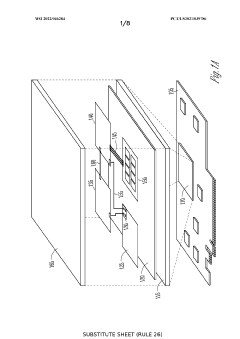
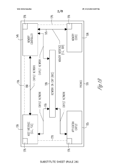
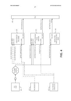
Method for configuring multiple input-output channels
PatentWO2022046284A1
Innovation
- The implementation of a Chiplet Protocol Interface (CPI) network with Advanced Interface Bus (AIB) channels and credit-based flow control, allowing for flexible virtual channel mapping and minimizing latency and energy consumption through packetized protocols and serialization-deserialization (SERDES) hardware, while enabling efficient inter-chiplet communication.
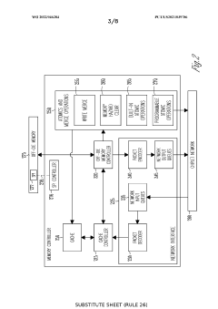
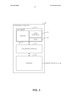
On-demand programmable atomic kernel loading
PatentWO2022086807A1
Innovation
- Implementing an on-demand mechanism for loading PAO kernels, where PAUs register for potential use and reserve space, loading the kernel only when requested, and signaling a trap to initiate kernel transfer when needed.
Standardization Efforts in Chiplet Technology
Standardization efforts in chiplet technology are crucial for ensuring interoperability and widespread adoption across the semiconductor industry. The development of common interfaces and protocols is essential for enabling seamless integration of chiplets from different manufacturers, fostering innovation, and reducing costs.
One of the most significant standardization initiatives is the Universal Chiplet Interconnect Express (UCIe) consortium. Formed by industry leaders such as Intel, AMD, Arm, and TSMC, UCIe aims to establish a universal interconnect standard for chiplets. This standard defines the physical and protocol layers for die-to-die interconnects, allowing chiplets from various vendors to communicate effectively within a single package.
The Open Compute Project (OCP) has also been instrumental in promoting chiplet standardization. Through its Open Domain-Specific Architecture (ODSA) subproject, OCP is working on developing open architectures and standards for chiplet-based systems. This effort includes the creation of reference designs, specifications for chiplet interfaces, and guidelines for thermal and power management.
Another important standardization effort is the CHIPS Alliance, which focuses on open-source hardware design and verification tools. The alliance is working on developing open-source implementations of chiplet interfaces and associated software stacks, making it easier for companies to adopt chiplet technology without relying solely on proprietary solutions.
The IEEE Standards Association has also recognized the importance of chiplet technology and has initiated working groups to develop standards for chiplet-based systems. These efforts include defining metrics for chiplet performance and reliability, as well as establishing guidelines for testing and qualification of chiplet-based products.
Standardization efforts extend beyond just interconnects and interfaces. There are ongoing initiatives to standardize packaging technologies, thermal management solutions, and power delivery systems for chiplet-based designs. Organizations like SEMI and JEDEC are actively involved in developing standards for advanced packaging technologies that are critical for chiplet integration.
As chiplet technology continues to evolve, these standardization efforts will play a crucial role in addressing challenges related to interoperability, scalability, and cost-effectiveness. By establishing common standards and protocols, the semiconductor industry can accelerate the adoption of chiplet-based designs and drive innovation in emerging computing technologies.
Economic Impact of Chiplet Adoption
The adoption of chiplet technology is poised to have a significant economic impact on the semiconductor industry and related sectors. This innovative approach to chip design and manufacturing addresses several key challenges in emerging computing technologies, offering substantial cost savings and improved performance.
Chiplets enable more efficient use of silicon wafers, reducing waste and lowering production costs. By allowing manufacturers to mix and match different components on a single package, chiplets optimize the use of advanced process nodes for critical components while utilizing older, more cost-effective nodes for less demanding functions. This flexibility in design and manufacturing can lead to substantial reductions in overall chip production expenses.
The modular nature of chiplets also contributes to improved yield rates. Instead of discarding entire large-scale integrated circuits due to defects, manufacturers can now isolate and replace faulty chiplets, significantly reducing waste and associated costs. This approach not only enhances production efficiency but also allows for more rapid iteration and time-to-market for new products.
Chiplet technology is expected to drive innovation and competition in the semiconductor industry. By lowering barriers to entry, smaller companies and startups can now focus on developing specialized chiplets rather than entire system-on-chip solutions. This democratization of chip design could lead to increased innovation and a more diverse ecosystem of semiconductor products and services.
The economic benefits of chiplets extend beyond the semiconductor industry. As chiplet-based designs enable more powerful and energy-efficient computing solutions, they are likely to accelerate advancements in artificial intelligence, edge computing, and high-performance computing. These technological improvements can drive productivity gains across various sectors, from healthcare and finance to manufacturing and transportation.
Moreover, the adoption of chiplets may reshape global supply chains in the semiconductor industry. As different components can be sourced from various manufacturers and integrated into a single package, chiplet technology could lead to a more distributed and resilient supply chain. This diversification may help mitigate risks associated with geopolitical tensions and supply chain disruptions.
In conclusion, the economic impact of chiplet adoption is expected to be far-reaching, offering cost savings, improved performance, and increased innovation in the semiconductor industry. As this technology matures and gains wider acceptance, it has the potential to drive significant economic growth and technological advancement across multiple sectors.
Unlock deeper insights with Patsnap Eureka Quick Research — get a full tech report to explore trends and direct your research. Try now!
Generate Your Research Report Instantly with AI Agent
Supercharge your innovation with Patsnap Eureka AI Agent Platform!