How to Implement Chiplet Solutions for Improved Signal Integrity?
JUL 16, 20259 MIN READ
Generate Your Research Report Instantly with AI Agent
Patsnap Eureka helps you evaluate technical feasibility & market potential.
Chiplet Technology Evolution and Objectives
Chiplet technology has emerged as a revolutionary approach in the semiconductor industry, addressing the challenges of traditional monolithic chip designs. The evolution of chiplet technology can be traced back to the early 2010s when semiconductor manufacturers began exploring modular chip designs to overcome the limitations of Moore's Law. The primary objective of chiplet technology is to improve performance, reduce costs, and enhance scalability in chip manufacturing.
The development of chiplet technology has been driven by the increasing demand for more powerful and efficient computing systems. As traditional chip scaling became more challenging and expensive, chiplet-based designs offered a viable alternative. By breaking down complex systems into smaller, more manageable components, chiplets allow for greater flexibility in chip design and manufacturing.
One of the key milestones in chiplet technology evolution was the introduction of advanced packaging techniques, such as 2.5D and 3D integration. These packaging methods enabled the integration of multiple chiplets on a single interposer or package substrate, facilitating high-bandwidth communication between different functional blocks. This approach significantly improved overall system performance while reducing power consumption and manufacturing costs.
The objectives of chiplet technology extend beyond mere performance improvements. They include enhancing yield rates, as smaller chiplets are less prone to manufacturing defects compared to large monolithic chips. Additionally, chiplet designs aim to improve time-to-market by allowing manufacturers to mix and match different functional blocks based on specific application requirements.
In the context of signal integrity, chiplet technology presents both opportunities and challenges. The primary goal is to maintain high-quality signal transmission between different chiplets and within the overall system. This objective involves minimizing signal degradation, reducing electromagnetic interference, and optimizing power delivery across the chiplet-based design.
As chiplet technology continues to evolve, researchers and engineers are focusing on developing advanced interconnect technologies and standardized interfaces. These efforts aim to facilitate seamless integration of chiplets from different manufacturers, promoting a more open and collaborative ecosystem in the semiconductor industry. The development of such standards is crucial for realizing the full potential of chiplet-based designs and ensuring interoperability across various platforms.
Looking ahead, the objectives of chiplet technology include pushing the boundaries of system integration, enabling more complex and powerful computing architectures, and supporting emerging applications in artificial intelligence, 5G communications, and high-performance computing. By addressing signal integrity challenges and refining interconnect technologies, chiplet solutions are poised to play a pivotal role in shaping the future of semiconductor design and manufacturing.
Market Demand for Advanced Chiplet Solutions
The market demand for advanced chiplet solutions has been steadily increasing in recent years, driven by the growing need for improved signal integrity in complex semiconductor designs. As traditional monolithic chip designs reach their physical and economic limits, chiplet-based architectures have emerged as a promising alternative to meet the ever-increasing performance and functionality requirements of modern electronic systems.
The semiconductor industry is experiencing a significant shift towards chiplet technology, with major players investing heavily in research and development. This trend is fueled by the demand for higher performance, lower power consumption, and reduced manufacturing costs. Chiplet solutions offer the flexibility to mix and match different process nodes and technologies, allowing for optimized designs that cater to specific market needs.
One of the key drivers for chiplet adoption is the need for improved signal integrity in high-speed communication interfaces. As data rates continue to increase, maintaining signal quality becomes increasingly challenging. Chiplet-based designs allow for shorter interconnects between functional blocks, reducing signal degradation and improving overall system performance. This is particularly crucial in applications such as data centers, 5G infrastructure, and high-performance computing, where data throughput and reliability are paramount.
The market for chiplet solutions is also being propelled by the growing demand for artificial intelligence and machine learning applications. These compute-intensive tasks require specialized accelerators and processors that can be efficiently integrated using chiplet technology. By combining different types of chiplets, such as CPUs, GPUs, and AI accelerators, manufacturers can create highly customized and optimized solutions for specific AI workloads.
Furthermore, the automotive industry is emerging as a significant market for advanced chiplet solutions. As vehicles become increasingly connected and autonomous, the demand for high-performance, low-power computing platforms is surging. Chiplet-based designs offer the flexibility and scalability needed to meet the diverse requirements of automotive applications, from infotainment systems to advanced driver assistance systems (ADAS).
The market demand for chiplet solutions is also driven by the need for more sustainable and energy-efficient computing. By enabling the integration of heterogeneous components and optimizing power consumption, chiplet-based designs can contribute to reducing the overall environmental impact of electronic systems. This aligns with the growing emphasis on green technology and sustainable practices across industries.
As the market for chiplet solutions continues to expand, there is an increasing focus on standardization and interoperability. Industry consortia and standards bodies are working towards developing common interfaces and protocols to facilitate the integration of chiplets from different vendors. This standardization effort is expected to further accelerate market adoption and drive innovation in chiplet-based designs.
Signal Integrity Challenges in Chiplet Design
Signal integrity challenges in chiplet design have become increasingly prominent as the semiconductor industry moves towards more modular and heterogeneous integration approaches. The chiplet architecture, which involves combining multiple smaller dies or "chiplets" on a single package, offers numerous advantages in terms of cost, yield, and flexibility. However, it also introduces complex signal integrity issues that must be addressed to ensure reliable high-speed communication between chiplets.
One of the primary challenges in chiplet design is managing signal degradation across the inter-chiplet interfaces. As signals traverse from one chiplet to another, they encounter various impedance discontinuities, crosstalk, and reflections that can significantly impact signal quality. These issues are exacerbated by the increasing data rates required for modern applications, pushing the limits of traditional interconnect technologies.
Another critical concern is the management of power delivery and thermal dissipation across the chiplet assembly. Uneven power distribution and localized heating can lead to voltage fluctuations and timing variations, further compromising signal integrity. The compact nature of chiplet designs also limits the space available for decoupling capacitors and other signal conditioning components, making it more challenging to maintain clean power and ground planes.
The diverse nature of chiplets, often manufactured using different process nodes or even by different vendors, introduces additional complexities in terms of signal level matching and timing synchronization. Ensuring consistent signal characteristics across heterogeneous interfaces requires careful consideration of voltage levels, impedance matching, and clock domain crossing strategies.
Electromagnetic interference (EMI) and electromagnetic compatibility (EMC) present another layer of challenges in chiplet designs. The close proximity of multiple high-speed interfaces can lead to unwanted coupling and radiation, potentially affecting both internal signals and compliance with regulatory standards. Shielding and isolation techniques must be carefully implemented to mitigate these effects without compromising the overall package density.
As chiplet designs push towards higher frequencies and wider bandwidths, the impact of package materials and manufacturing tolerances on signal integrity becomes more pronounced. Variations in dielectric properties, conductor geometries, and via structures can significantly affect signal propagation characteristics, necessitating advanced modeling and simulation techniques to predict and mitigate these effects.
Addressing these signal integrity challenges requires a holistic approach that encompasses both chip-level and package-level design considerations. Advanced signaling techniques such as equalization, pre-emphasis, and de-emphasis are often employed to compensate for channel losses and improve signal quality. Additionally, the development of specialized interconnect technologies, such as advanced organic substrates and silicon interposers, plays a crucial role in enabling high-bandwidth, low-loss communication between chiplets.
Current Signal Integrity Solutions for Chiplets
01 Signal integrity optimization in chiplet interconnects
Techniques for optimizing signal integrity in chiplet-based designs, focusing on interconnect technologies and signal transmission methods between chiplets. This includes advanced packaging solutions, high-speed SerDes implementations, and innovative routing strategies to minimize signal degradation and maintain data integrity across chiplet interfaces.- Signal integrity optimization in chiplet interconnects: Techniques for optimizing signal integrity in chiplet-based designs, focusing on interconnect design, signal routing, and impedance matching. These methods aim to reduce signal distortion, crosstalk, and reflections in high-speed data transmission between chiplets, ensuring reliable communication within multi-chip modules.
- Advanced packaging solutions for chiplets: Innovative packaging technologies designed specifically for chiplet integration, addressing signal integrity challenges. These solutions may include advanced interposers, through-silicon vias (TSVs), and novel substrate materials that help maintain signal quality across chiplet interfaces while enabling high-density interconnects.
- Signal conditioning and equalization for chiplet interfaces: Implementation of signal conditioning and equalization techniques at chiplet interfaces to compensate for channel losses and improve signal integrity. This may include pre-emphasis, de-emphasis, and adaptive equalization methods to enhance signal quality in high-speed chiplet-to-chiplet communications.
- Power integrity and signal integrity co-optimization: Strategies for simultaneously optimizing power and signal integrity in chiplet designs. This approach considers the interdependence of power distribution networks and signal paths, aiming to minimize noise coupling and maintain clean power delivery, which is crucial for preserving signal integrity across chiplet interfaces.
- Test and verification methods for chiplet signal integrity: Development of specialized test and verification methodologies for assessing and ensuring signal integrity in chiplet-based systems. These methods may include on-chip monitoring, high-speed serial link characterization, and advanced simulation techniques to validate signal quality across chiplet interfaces under various operating conditions.
02 Power distribution network design for chiplets
Strategies for designing efficient power distribution networks in chiplet architectures to ensure stable power delivery and minimize noise. This encompasses techniques for on-chip and off-chip power regulation, decoupling capacitor placement, and innovative power plane designs to support high-performance chiplet solutions while maintaining signal integrity.Expand Specific Solutions03 Electromagnetic interference (EMI) mitigation in chiplet designs
Methods for reducing electromagnetic interference in chiplet-based systems to improve overall signal integrity. This includes shielding techniques, ground plane optimization, and innovative packaging materials to minimize crosstalk and other EMI-related issues in densely packed chiplet arrangements.Expand Specific Solutions04 Clock distribution and synchronization for chiplets
Techniques for efficient clock distribution and synchronization across multiple chiplets to maintain timing integrity and reduce skew. This involves advanced clock tree synthesis methods, adaptive clocking schemes, and innovative synchronization protocols tailored for chiplet-based architectures.Expand Specific Solutions05 Thermal management for signal integrity in chiplet solutions
Approaches to thermal management in chiplet designs to maintain signal integrity under varying temperature conditions. This includes advanced cooling solutions, thermal-aware placement and routing strategies, and dynamic thermal management techniques to ensure consistent signal quality across chiplet interfaces.Expand Specific Solutions
Key Players in Chiplet Industry
The implementation of chiplet solutions for improved signal integrity is currently in a transitional phase, with the market showing significant growth potential. The technology is advancing rapidly, driven by the need for enhanced performance and efficiency in complex semiconductor designs. Major players like Intel, AMD, and TSMC are at the forefront, investing heavily in chiplet technology. Huawei and IBM are also making strides in this area, while companies such as Micron and Samsung are exploring chiplet solutions for memory applications. The market is expected to expand as more companies recognize the benefits of chiplet architecture in addressing signal integrity challenges and improving overall system performance.
Huawei Technologies Co., Ltd.
Technical Solution: Huawei's chiplet solution for improved signal integrity revolves around their Kirin series SoCs and advanced packaging technologies. They have developed a chiplet-based architecture that utilizes high-bandwidth interconnects and 2.5D packaging techniques to optimize signal integrity[7]. Huawei's approach includes the use of through-silicon vias (TSVs) and micro-bumps for vertical integration, reducing signal path lengths and minimizing signal degradation. Their chiplet designs incorporate advanced power delivery networks and sophisticated signal conditioning circuits to maintain signal quality across high-speed interfaces[8]. Huawei has also invested in developing proprietary interconnect technologies and signal processing algorithms to further enhance signal integrity in their multi-chip modules.
Strengths: Advanced packaging techniques, high-bandwidth interconnects, and proprietary signal processing algorithms. Weaknesses: Potential geopolitical challenges affecting global adoption and supply chain issues.
Intel Corp.
Technical Solution: Intel's chiplet solution for improved signal integrity focuses on their Embedded Multi-die Interconnect Bridge (EMIB) technology. EMIB uses a small silicon bridge embedded in the package substrate to connect multiple chiplets, allowing high-bandwidth connections with shorter trace lengths[1]. This approach reduces signal degradation and improves overall system performance. Intel has also implemented advanced packaging technologies like Foveros, which uses 3D stacking to further enhance signal integrity[2]. Their chiplets are connected using through-silicon vias (TSVs) and micro-bumps, enabling high-density interconnects with minimal signal loss. Intel's solution also incorporates advanced power delivery networks and thermal management techniques to maintain signal quality across the chiplet architecture[3].
Strengths: High-bandwidth connections, reduced signal degradation, and flexibility in chip design. Weaknesses: Complexity in manufacturing and potential thermal challenges in 3D stacked designs.
Innovative Interconnect Technologies
SGS or gsgsg pattern for signal transmitting channel, and PCB assembly, chip package using such SGS or gsgsg pattern
PatentActiveUS20160120034A1
Innovation
- The implementation of a SGS or GSGSG channel circuit design in printed circuit boards and chip packages, featuring a pair of differential signal traces sandwiched by ground guard lines and an intervening reference trace, which helps in achieving the required impedance matching for high-speed signal transmission, conforming to specifications like MHL, using a cost-effective 2-layer PCB without sacrificing routing space.
Semiconductor package with RFIC and antenna
PatentPendingUS20250112357A1
Innovation
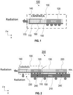
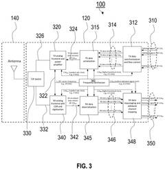
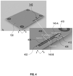
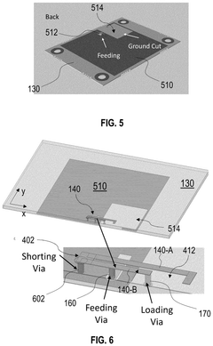
- The integration of a radio frequency integrated circuit (RFIC) and a compact mm-wave antenna within a semiconductor package, which enables wireless communication between chiplets, packages, and motherboards, thereby reducing the need for physical routing and alleviating congestion in I/O escape routes.
Thermal Management in Chiplet Designs
Thermal management is a critical aspect of chiplet designs, particularly as the industry moves towards more complex and densely packed multi-chip modules. The integration of multiple chiplets in a single package presents unique thermal challenges that must be addressed to ensure optimal performance and reliability.
One of the primary concerns in chiplet thermal management is the increased power density resulting from the close proximity of multiple high-performance dies. This concentration of heat-generating components can lead to localized hotspots, which may cause thermal throttling or even permanent damage if not properly managed. To mitigate these issues, designers are implementing advanced cooling solutions that target both the package and system levels.
At the package level, thermal interface materials (TIMs) play a crucial role in efficiently transferring heat from the chiplets to the heat spreader. High-performance TIMs with improved thermal conductivity and reduced thermal resistance are being developed to enhance heat dissipation. Additionally, advanced heat spreader designs, such as vapor chambers or micro-channel liquid cooling integrated directly into the package, are being explored to provide more effective heat distribution.
System-level cooling solutions are also evolving to accommodate the thermal demands of chiplet designs. Enhanced air cooling systems with optimized heatsink designs and high-performance fans are being employed for moderate thermal loads. For more demanding applications, liquid cooling solutions, including both single-phase and two-phase systems, are gaining traction due to their superior heat transfer capabilities.
The thermal management strategy for chiplet designs must also consider the impact of non-uniform heat generation across the package. Different chiplets may have varying power profiles, leading to temperature gradients that can affect signal integrity and overall system performance. To address this, designers are implementing dynamic thermal management techniques that utilize on-chip temperature sensors and intelligent power management algorithms to balance thermal loads across the chiplets.
Furthermore, the development of advanced packaging technologies, such as 2.5D and 3D integration, introduces additional thermal considerations. These technologies often involve the use of interposers or through-silicon vias (TSVs), which can impact heat flow paths and create new thermal challenges. Innovative cooling solutions, such as inter-layer cooling for 3D stacked dies, are being researched to address these specific thermal management requirements.
As chiplet designs continue to evolve, thermal simulation and modeling tools are becoming increasingly sophisticated. These tools enable designers to predict and optimize thermal performance early in the design process, reducing development time and costs. By leveraging accurate thermal models, engineers can evaluate various cooling strategies and make informed decisions on thermal management solutions that best suit their specific chiplet designs.
Standardization Efforts for Chiplet Interfaces
The standardization of chiplet interfaces is a critical aspect of implementing chiplet solutions for improved signal integrity. As the chiplet ecosystem continues to grow, industry-wide efforts are underway to establish common standards that ensure interoperability and optimize performance across different chiplet designs.
One of the most prominent standardization initiatives is the Universal Chiplet Interconnect Express (UCIe) consortium. Launched in 2022, UCIe aims to create an open industry standard for die-to-die interconnects. The consortium includes major players such as Intel, AMD, Arm, TSMC, and Samsung, among others. UCIe focuses on defining a standardized die-to-die interconnect that covers multiple layers of the interconnect stack, including the physical layer, protocol layer, and software layer.
Another significant standardization effort is the Open Compute Project's (OCP) Chiplet Design Exchange (CDX) working group. CDX is developing a set of open specifications for chiplet-based designs, focusing on areas such as thermal management, power delivery, and signal integrity. The group aims to create a standardized approach to chiplet integration that can be adopted across the industry.
The JEDEC Solid State Technology Association has also been active in chiplet standardization. Their JC-42 Committee on High-Bandwidth Memory (HBM) has been working on standards for chiplet-to-chiplet and chiplet-to-package substrate interconnects. These standards are crucial for ensuring consistent performance and reliability in high-bandwidth memory applications using chiplet technology.
In addition to these consortia-led efforts, individual companies are also contributing to standardization through open-source initiatives. For example, Intel's Advanced Interface Bus (AIB) and Bunch of Wires (BoW) interface specifications have been released as open standards, allowing other companies to adopt and build upon these technologies.
The IEEE Standards Association has also recognized the importance of chiplet standardization. They have initiated the development of IEEE P3094, a standard for interoperable multi-die systems. This standard aims to address the challenges of integrating heterogeneous chiplets from different vendors, focusing on aspects such as physical interfaces, protocols, and testing methodologies.
These standardization efforts are crucial for the widespread adoption of chiplet technology and the improvement of signal integrity in multi-die systems. By establishing common interfaces and protocols, these standards will enable designers to mix and match chiplets from different vendors, reduce development costs, and accelerate time-to-market for new products. As these standards mature, they will play a pivotal role in shaping the future of chiplet-based system design and manufacturing.
Unlock deeper insights with Patsnap Eureka Quick Research — get a full tech report to explore trends and direct your research. Try now!
Generate Your Research Report Instantly with AI Agent
Supercharge your innovation with Patsnap Eureka AI Agent Platform!