

How Chiplets Simplify High-Performance Computing Designs?
JUL 16, 20259 MIN READ
Generate Your Research Report Instantly with AI Agent
PatSnap Eureka helps you evaluate technical feasibility & market potential.
Chiplet Technology Evolution and Objectives
Chiplet technology has emerged as a revolutionary approach in the field of high-performance computing (HPC) design, marking a significant shift from traditional monolithic chip architectures. The evolution of chiplets can be traced back to the early 2010s when semiconductor manufacturers began exploring ways to overcome the limitations of Moore's Law and address the increasing complexity of chip design.
The primary objective of chiplet technology is to simplify HPC designs by breaking down complex systems into smaller, more manageable components. This approach allows for greater flexibility, improved yield, and enhanced performance while reducing costs associated with large-scale chip production. By enabling the integration of diverse components from different process nodes, chiplets offer a pathway to continue scaling performance beyond the constraints of traditional monolithic designs.
The evolution of chiplet technology has been driven by several key factors. First, the slowing pace of Moore's Law has necessitated alternative approaches to improving chip performance and efficiency. Second, the increasing demand for specialized computing solutions in areas such as artificial intelligence, machine learning, and data analytics has created a need for more flexible and customizable chip designs. Finally, the rising costs associated with developing and manufacturing cutting-edge monolithic chips have pushed the industry towards more cost-effective solutions.
Throughout its development, chiplet technology has seen several significant milestones. The introduction of 2.5D and 3D packaging technologies has been crucial in enabling the effective integration of multiple chiplets. Advanced interconnect technologies, such as Intel's EMIB (Embedded Multi-die Interconnect Bridge) and TSMC's CoWoS (Chip on Wafer on Substrate), have played a vital role in facilitating high-bandwidth, low-latency communication between chiplets.
The objectives of chiplet technology in simplifying HPC designs are multifaceted. One primary goal is to improve overall system performance by allowing the integration of best-in-class components, each optimized for specific functions. This modular approach enables designers to mix and match different process nodes and technologies within a single package, leading to enhanced performance and power efficiency.
Another key objective is to reduce manufacturing costs and improve yield rates. By breaking down complex designs into smaller, more manageable chiplets, manufacturers can achieve higher yields and lower production costs compared to large monolithic chips. This approach also allows for greater reuse of proven designs, further streamlining the development process and reducing time-to-market for new products.
Looking ahead, the future objectives of chiplet technology include further advancements in interconnect technologies, standardization of chiplet interfaces, and the development of more sophisticated design and integration tools. These efforts aim to create a more robust ecosystem for chiplet-based designs, enabling even greater flexibility and innovation in HPC systems.
HPC Market Demand Analysis
The high-performance computing (HPC) market has been experiencing significant growth and transformation, driven by the increasing demand for advanced computational capabilities across various industries. As organizations seek to tackle complex problems and process massive datasets, the need for more powerful and efficient HPC solutions has become paramount.
The global HPC market is projected to expand rapidly in the coming years, with a compound annual growth rate (CAGR) exceeding 6% from 2021 to 2026. This growth is fueled by the adoption of HPC systems in sectors such as scientific research, financial services, healthcare, and manufacturing. The rise of artificial intelligence and machine learning applications has further accelerated the demand for HPC solutions capable of handling intensive computational workloads.
One of the key drivers of market demand is the need for improved energy efficiency and performance in HPC systems. As data centers face increasing pressure to reduce their carbon footprint and operational costs, there is a growing emphasis on developing more power-efficient computing solutions. This has led to a surge in interest in innovative technologies like chiplets, which offer the potential to optimize performance while minimizing power consumption.
The healthcare and life sciences sectors have emerged as significant contributors to HPC market growth. The ongoing COVID-19 pandemic has highlighted the critical role of HPC in accelerating drug discovery, vaccine development, and genomic research. As a result, there is a heightened focus on deploying HPC systems capable of processing vast amounts of biological data and running complex simulations.
In the financial services industry, HPC solutions are becoming increasingly crucial for risk management, algorithmic trading, and fraud detection. The ability to process and analyze large volumes of financial data in real-time has become a competitive advantage, driving the adoption of advanced HPC systems among banks, hedge funds, and insurance companies.
The manufacturing sector is another key driver of HPC market demand, particularly in the automotive and aerospace industries. As these sectors embrace digital transformation and Industry 4.0 initiatives, there is a growing need for HPC solutions to support complex simulations, design optimization, and virtual prototyping. This trend is expected to continue as manufacturers seek to reduce time-to-market and improve product quality through advanced computational techniques.
As the demand for HPC solutions continues to grow, there is an increasing focus on developing more scalable and flexible architectures. This has led to a rising interest in disaggregated computing models, where different components of the system can be upgraded or replaced independently. Chiplet technology aligns well with this trend, offering the potential for more modular and customizable HPC designs that can be tailored to specific application requirements.
Chiplet Integration Challenges
While chiplets offer significant advantages in high-performance computing designs, their integration presents several challenges that need to be addressed. One of the primary obstacles is the interconnect technology required to link multiple chiplets effectively. Traditional package-level interconnects often lack the bandwidth and energy efficiency necessary for high-performance chiplet-based systems. This has led to the development of advanced interconnect technologies, such as silicon interposers and organic substrates with fine-pitch routing, which can support higher data rates and lower power consumption.
Another critical challenge is thermal management. As chiplets are packed closely together, heat dissipation becomes a significant concern. The compact nature of chiplet designs can create hotspots that are difficult to cool effectively, potentially leading to performance degradation or reliability issues. Innovative cooling solutions, such as integrated liquid cooling or advanced heat spreaders, are being explored to address this challenge.
Signal integrity and power delivery also pose significant hurdles in chiplet integration. The high-speed signals traveling between chiplets are susceptible to interference and signal degradation, which can impact system performance. Careful design of signal paths, impedance matching, and advanced packaging techniques are crucial to maintaining signal integrity. Additionally, delivering clean and stable power to each chiplet in a multi-die package requires sophisticated power distribution networks and decoupling strategies.
Testing and yield management present unique challenges in chiplet-based designs. Traditional testing methods may not be sufficient for identifying defects in individual chiplets or in the interconnects between them. New testing methodologies and equipment are needed to ensure the reliability and performance of chiplet-based systems. Furthermore, managing yield becomes more complex as the number of chiplets in a package increases, requiring advanced binning and matching techniques to optimize overall system yield.
Standardization is another significant challenge in the chiplet ecosystem. The lack of universal standards for chiplet interfaces and packaging can hinder interoperability and limit the potential for mix-and-match designs from different vendors. Industry consortia and standardization efforts, such as the Universal Chiplet Interconnect Express (UCIe), are working to address this issue by developing common specifications for chiplet integration.
Lastly, the design and verification process for chiplet-based systems is more complex than traditional monolithic designs. Engineers must consider the interactions between multiple chiplets, optimize the overall system architecture, and verify the functionality of the integrated package. This requires new design tools, methodologies, and expertise to effectively manage the increased complexity of chiplet-based designs.
Current Chiplet Design Solutions
01 Modular chiplet design and integration
Chiplet technology allows for modular design and integration of different functional blocks. This approach simplifies the overall chip design process by enabling the use of pre-designed and pre-verified chiplets, which can be combined to create more complex systems. This modular approach reduces development time and costs while improving flexibility and scalability.- Modular chiplet design and integration: Chiplet technology allows for modular design and integration of different functional blocks. This approach simplifies the overall chip design process by enabling the use of pre-designed and pre-verified chiplets, which can be combined to create more complex systems. This modular approach reduces development time and costs while improving flexibility and scalability.
- Interconnect optimization for chiplets: Simplifying chiplet designs involves optimizing the interconnects between different chiplets. This includes developing efficient communication protocols, reducing signal latency, and minimizing power consumption in inter-chiplet connections. Advanced packaging technologies and high-bandwidth interfaces are utilized to enhance the overall performance of multi-chiplet systems.
- Thermal management and power optimization: Chiplet simplification involves addressing thermal challenges and optimizing power distribution across multiple chiplets. This includes developing advanced cooling solutions, implementing efficient power delivery networks, and utilizing power gating techniques to manage heat dissipation and energy consumption in chiplet-based designs.
- Standardization and interoperability of chiplets: Efforts to simplify chiplet integration focus on developing industry standards for chiplet interfaces and protocols. This standardization enables interoperability between chiplets from different manufacturers, simplifying the design and integration process. It also promotes the creation of a diverse ecosystem of chiplet suppliers and accelerates the adoption of chiplet technology.
- Design automation and verification for chiplets: Simplifying chiplet-based system design involves developing advanced EDA tools and methodologies. These tools automate the process of chiplet selection, placement, and integration, while also providing comprehensive verification and validation capabilities. This automation reduces design complexity, improves time-to-market, and ensures the reliability of chiplet-based systems.
02 Interconnect optimization for chiplets
Simplifying chiplet designs involves optimizing the interconnects between different chiplets. This includes developing efficient communication protocols, reducing signal latency, and minimizing power consumption in inter-chiplet connections. Advanced packaging technologies and high-bandwidth interfaces are utilized to improve overall system performance and reduce complexity.Expand Specific Solutions03 Standardization of chiplet interfaces
Standardizing chiplet interfaces is crucial for simplifying chiplet-based designs. This involves creating common protocols and specifications for chiplet-to-chiplet communication, power delivery, and thermal management. Standardization enables easier integration of chiplets from different vendors and reduces design complexity for system integrators.Expand Specific Solutions04 Automated design and verification tools for chiplets
Development of specialized EDA (Electronic Design Automation) tools for chiplet-based designs simplifies the design and verification process. These tools automate tasks such as chiplet placement, routing, and system-level optimization. They also facilitate rapid prototyping and testing of chiplet-based systems, reducing time-to-market and design complexity.Expand Specific Solutions05 Thermal and power management for chiplet systems
Simplifying chiplet designs involves addressing thermal and power management challenges. This includes developing efficient cooling solutions, optimizing power distribution networks, and implementing advanced power management techniques. These approaches help in maintaining system stability and performance while reducing overall design complexity and improving energy efficiency.Expand Specific Solutions
Key Chiplet Technology Players
The chiplet technology market is in a growth phase, with major players actively developing and implementing solutions to address high-performance computing challenges. The market size is expanding rapidly as chiplets offer a cost-effective approach to scaling semiconductor performance. Technologically, chiplets are maturing, with companies like Intel, AMD, and TSMC leading the way in implementation. These firms, along with others such as Micron and GlobalFoundries, are investing heavily in chiplet-based designs to overcome limitations in traditional monolithic chip architectures. The competitive landscape is dynamic, with both established semiconductor giants and innovative startups like Primemas contributing to advancements in chiplet technology, driving efficiency and performance improvements in high-performance computing designs.
Intel Corp.
Technical Solution: Intel's chiplet approach, known as "Foveros" technology, enables 3D stacking of chiplets[1]. This allows for the integration of different process nodes and IP blocks in a single package. Intel's Ponte Vecchio GPU, designed for high-performance computing and AI, utilizes over 40 chiplets manufactured on different process nodes[2]. The company also employs their Advanced Interface Bus (AIB) for high-bandwidth, low-power die-to-die communication between chiplets[3]. Intel's chiplet strategy aims to improve yield, reduce costs, and enhance performance scalability in complex computing systems.
Strengths: Flexibility in combining different process nodes, improved yield, and cost-effectiveness. Weaknesses: Increased complexity in system integration and thermal management.
Taiwan Semiconductor Manufacturing Co., Ltd.
Technical Solution: TSMC's chiplet solution, called System on Integrated Chips (SoIC), uses advanced packaging technologies like Chip on Wafer on Substrate (CoWoS) and Integrated Fan-Out (InFO)[4]. Their 3DFabric technology enables the integration of heterogeneous chiplets in both 2.5D and 3D configurations[5]. TSMC's approach allows for the combination of logic dies, high-bandwidth memory, and I/O chiplets in a single package, catering to high-performance computing needs. The company's advanced packaging solutions support chiplet-based designs with high-density interconnects and improved thermal management[6].
Strengths: Advanced packaging technologies, high-density interconnects, and support for heterogeneous integration. Weaknesses: Potential for higher manufacturing costs and complexity in supply chain management.
Innovative Chiplet Interconnect Technologies
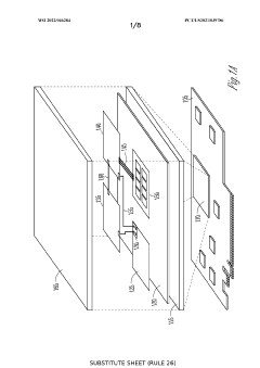
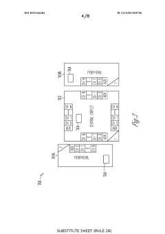
Method for configuring multiple input-output channels
PatentWO2022046284A1
Innovation
- The implementation of a Chiplet Protocol Interface (CPI) network with Advanced Interface Bus (AIB) channels and credit-based flow control, allowing for flexible virtual channel mapping and minimizing latency and energy consumption through packetized protocols and serialization-deserialization (SERDES) hardware, while enabling efficient inter-chiplet communication.
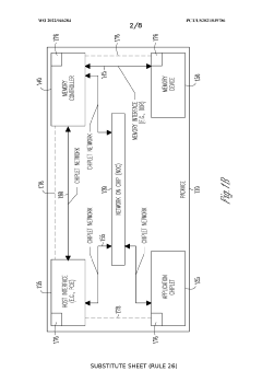
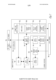
Edge interface placements to enable chiplet rotation into multi-chiplet cluster
PatentPendingUS20240332257A1
Innovation
- The implementation of a chiplet architecture that uses a network-on-chip (NOC) with a chiplet protocol interface (CPI) to facilitate high-speed, flexible inter-chiplet communication, combined with a tightly packed matrix arrangement of chiplets and I/O micro-bumps for close-coupled interconnects, allowing for proper alignment and minimal footprint.
Thermal Management in Chiplet-based HPC
Thermal management is a critical aspect of chiplet-based High-Performance Computing (HPC) designs. As chiplets allow for the integration of multiple specialized dies on a single package, they introduce unique thermal challenges that must be addressed to ensure optimal performance and reliability.
One of the primary thermal management considerations in chiplet-based HPC is the increased power density. With multiple high-performance dies packed closely together, the heat generated per unit area is significantly higher than in traditional monolithic designs. This concentration of heat sources requires advanced cooling solutions to maintain acceptable operating temperatures.
Heterogeneous integration in chiplet designs also leads to non-uniform heat distribution across the package. Different chiplets may have varying power consumption and thermal characteristics, resulting in localized hotspots. These thermal gradients can cause mechanical stress and potentially impact the reliability and performance of the system.
To address these challenges, several thermal management strategies have been developed for chiplet-based HPC systems. Advanced packaging technologies, such as silicon interposers and through-silicon vias (TSVs), play a crucial role in heat dissipation. These technologies enable better thermal conductivity between chiplets and the package substrate, facilitating more efficient heat removal.
Active cooling solutions, including liquid cooling and microfluidic channels, are increasingly being employed in chiplet-based HPC designs. These techniques offer superior heat dissipation capabilities compared to traditional air cooling, allowing for higher power densities and improved thermal management.
Thermal-aware design methodologies are also essential in chiplet-based HPC. This involves careful consideration of chiplet placement, power distribution, and thermal interfaces during the design phase. Sophisticated thermal modeling and simulation tools are used to optimize the thermal performance of the overall system.
Dynamic thermal management techniques, such as adaptive clock gating and power gating, are implemented at the system level to manage heat generation in real-time. These techniques allow for fine-grained control of power consumption and heat generation across different chiplets, helping to maintain optimal thermal conditions during operation.
As chiplet-based HPC designs continue to evolve, ongoing research focuses on developing novel thermal management solutions. These include advanced materials with superior thermal properties, 3D-stacked chiplet architectures with integrated cooling layers, and AI-driven thermal management algorithms that can predict and mitigate thermal issues proactively.
Standardization Efforts in Chiplet Ecosystem
Standardization efforts in the chiplet ecosystem are crucial for enabling interoperability and fostering innovation in high-performance computing designs. The development of industry-wide standards is essential to ensure that chiplets from different manufacturers can seamlessly integrate and function together within a single package.
One of the most significant standardization initiatives is the Universal Chiplet Interconnect Express (UCIe) consortium. Formed by leading technology companies, UCIe aims to establish a common interconnect standard for chiplets. This standard defines protocols, electrical interfaces, and physical specifications to facilitate communication between different chiplets, regardless of their origin or manufacturer.
The Advanced Interface Bus (AIB) is another important standardization effort. Developed by Intel and later released as an open standard, AIB provides a die-to-die interconnect protocol that enables high-bandwidth, low-latency communication between chiplets. This standard has been adopted by several companies and is contributing to the broader adoption of chiplet-based designs.
The Open Compute Project (OCP) has also been actively involved in chiplet standardization. Through its Open Domain-Specific Architecture (ODSA) subproject, OCP is working on developing open architectures and standards for chiplet-based systems. This initiative aims to create a more open and collaborative ecosystem for chiplet development and integration.
Standardization efforts extend beyond interconnects to include packaging technologies. The Joint Electron Device Engineering Council (JEDEC) has been working on standards for advanced packaging, including those relevant to chiplet integration. These standards address issues such as thermal management, signal integrity, and power delivery in multi-chip packages.
The Heterogeneous Integration Roadmap (HIR), sponsored by IEEE, SEMI, and other organizations, provides a long-term vision for standardization in chiplet technologies. It outlines the technical challenges and potential solutions for integrating diverse chiplets, guiding the industry towards common goals and standards.
As the chiplet ecosystem continues to evolve, these standardization efforts play a vital role in simplifying high-performance computing designs. They enable designers to mix and match chiplets from different vendors, reduce development costs, and accelerate time-to-market for new products. The ongoing collaboration between industry leaders, research institutions, and standards bodies is essential for the continued growth and success of chiplet-based architectures in high-performance computing.
Unlock deeper insights with PatSnap Eureka Quick Research — get a full tech report to explore trends and direct your research. Try now!
Generate Your Research Report Instantly with AI Agent
Supercharge your innovation with PatSnap Eureka AI Agent Platform!