

Chiplet Design for Best-in-Class Software Integration
JUL 16, 20259 MIN READ
Generate Your Research Report Instantly with AI Agent
PatSnap Eureka helps you evaluate technical feasibility & market potential.
Chiplet Design Evolution
Chiplet design has undergone significant evolution since its inception, driven by the need for more efficient and scalable semiconductor solutions. The journey began with the concept of disaggregating large monolithic chips into smaller, more manageable components. This approach emerged as a response to the challenges posed by Moore's Law, which was becoming increasingly difficult and expensive to maintain in traditional chip design.
In the early stages, chiplet design focused primarily on physical disaggregation, with limited consideration for software integration. The primary goal was to improve manufacturing yields and reduce costs by separating complex chip designs into smaller, more easily producible parts. This phase saw the development of basic interconnect technologies to allow communication between chiplets.
As the technology matured, the focus shifted towards more sophisticated integration techniques. The introduction of advanced packaging technologies, such as 2.5D and 3D integration, allowed for higher bandwidth and lower latency communication between chiplets. This phase also saw the development of standardized interfaces, which began to address the challenges of software integration across different chiplet components.
The next significant evolution came with the recognition of the importance of software-hardware co-design in chiplet architectures. This phase saw the development of more sophisticated on-chip and off-chip communication protocols, designed to facilitate seamless software integration across heterogeneous chiplets. The industry began to focus on creating standardized software abstractions that could work across different chiplet configurations.
Recent advancements have pushed chiplet design towards a more holistic approach, considering software integration from the earliest stages of hardware design. This has led to the development of chiplet architectures specifically optimized for software performance, with features such as cache coherency across chiplets, unified memory architectures, and hardware-level support for virtualization and security.
The latest trend in chiplet design evolution is the move towards AI-optimized architectures. This involves creating specialized chiplets for AI workloads that can be seamlessly integrated with general-purpose computing chiplets. The focus is on developing software frameworks that can efficiently distribute AI workloads across these heterogeneous chiplet systems, maximizing performance and energy efficiency.
Looking forward, the evolution of chiplet design is expected to continue towards even greater levels of software-hardware integration. This may include the development of reconfigurable chiplet architectures that can adapt to different software requirements in real-time, as well as the integration of advanced memory technologies directly into chiplet designs to further optimize software performance.
Software Integration Market
The software integration market for chiplet design is experiencing significant growth and transformation, driven by the increasing complexity of modern computing systems and the demand for more efficient, scalable, and customizable solutions. As chiplet technology gains traction in the semiconductor industry, the need for advanced software integration tools and methodologies has become paramount.
The market for software integration in chiplet design encompasses a wide range of solutions, including electronic design automation (EDA) tools, simulation software, and verification platforms. These tools are essential for enabling seamless integration of multiple chiplets into a single package, ensuring optimal performance, power efficiency, and reliability. The market is characterized by a mix of established EDA vendors and emerging startups specializing in chiplet-specific integration solutions.
One of the key drivers of this market is the growing adoption of heterogeneous computing architectures, which combine different types of processing units on a single package. This trend has led to increased demand for software tools that can effectively manage the integration of diverse chiplets, each potentially utilizing different process nodes or technologies. The market is also influenced by the need for improved time-to-market and cost-effectiveness in semiconductor design and manufacturing.
The software integration market for chiplet design is closely tied to advancements in packaging technologies, such as 2.5D and 3D integration. As these packaging techniques evolve, software tools must adapt to support new design paradigms and address challenges related to thermal management, signal integrity, and power distribution across multiple chiplets.
Geographically, the market shows strong presence in regions with established semiconductor ecosystems, including North America, East Asia, and Europe. However, emerging markets in other parts of Asia and the Middle East are also showing increased interest and investment in chiplet technologies and related software integration solutions.
The market is characterized by a high degree of innovation and rapid technological advancement. Companies are investing heavily in research and development to create more sophisticated integration tools that can handle the increasing complexity of chiplet-based designs. This includes the development of AI-powered design automation tools, advanced simulation capabilities, and improved interoperability between different chiplet technologies.
As the chiplet ecosystem continues to mature, the software integration market is expected to expand further, with new opportunities emerging in areas such as cloud-based design platforms, open-source integration frameworks, and specialized tools for specific application domains like high-performance computing, automotive, and edge AI. The market's growth is also likely to be influenced by industry standardization efforts, which aim to establish common interfaces and protocols for chiplet integration.
Chiplet Challenges
Chiplet design presents several significant challenges that must be addressed to achieve optimal software integration. One of the primary obstacles is the complexity of inter-chiplet communication. As chiplets are essentially separate dies integrated onto a single package, ensuring seamless and efficient data transfer between these components is crucial. This requires sophisticated interconnect technologies and protocols that can handle high-bandwidth, low-latency communication while minimizing power consumption.
Another major challenge lies in thermal management. The dense integration of multiple chiplets can lead to increased heat generation, potentially affecting performance and reliability. Designers must develop innovative cooling solutions and thermal dissipation strategies to maintain optimal operating temperatures across the entire package. This may involve advanced packaging materials, novel heat spreader designs, or even liquid cooling techniques for high-performance applications.
Power distribution and management pose additional hurdles in chiplet design. Each chiplet may have different power requirements, and ensuring stable power delivery across the entire system can be complex. This necessitates careful power domain planning, efficient voltage regulation, and intelligent power gating mechanisms to optimize energy consumption without compromising performance.
The heterogeneous nature of chiplet-based systems also presents challenges in terms of design and verification. Integrating chiplets from different vendors or with varying process nodes requires robust interface standards and comprehensive testing methodologies. Ensuring compatibility and proper functionality across diverse components demands extensive simulation, emulation, and physical testing, which can significantly increase development time and costs.
Software integration for chiplet-based systems introduces its own set of challenges. The distributed nature of processing elements across multiple chiplets requires sophisticated software architectures that can efficiently manage workload distribution, memory access, and inter-chiplet communication. Developing operating systems, drivers, and middleware that can fully leverage the potential of chiplet-based hardware while maintaining compatibility with existing software ecosystems is a complex undertaking.
Lastly, manufacturing and yield management for chiplet designs present unique challenges. The assembly process for multi-chiplet packages requires precise alignment and bonding techniques. Additionally, ensuring consistent quality and yield across different chiplets can be more challenging than traditional monolithic designs. This may necessitate new testing and quality control procedures throughout the manufacturing and packaging processes.
Current Chiplet Solutions
01 Integrated Design Environment for Chiplets
Software platforms that provide a comprehensive environment for designing and integrating chiplets. These tools offer features for layout, simulation, and verification of multi-chip modules, enabling seamless collaboration between different design teams and efficient management of complex chiplet-based systems.- Integrated design environments for chiplets: Software platforms that provide comprehensive tools for designing, simulating, and integrating chiplets. These environments offer features like layout design, performance analysis, and compatibility checks to streamline the chiplet development process.
- Automated chiplet integration and optimization: AI-driven software solutions that automate the process of integrating multiple chiplets into a cohesive system. These tools optimize interconnects, power distribution, and thermal management across chiplets to enhance overall system performance.
- Chiplet design verification and validation: Software tools focused on verifying and validating chiplet designs before fabrication. These solutions perform comprehensive checks on signal integrity, power integrity, and thermal analysis to ensure chiplet compatibility and system-level performance.
- Interoperability standards for chiplet design: Software frameworks and tools that implement and enforce interoperability standards for chiplet design. These solutions ensure that chiplets from different vendors can seamlessly integrate and communicate within a single system.
- Chiplet-aware EDA tools: Enhanced electronic design automation (EDA) tools that are specifically tailored for chiplet-based designs. These tools incorporate chiplet-specific considerations into traditional EDA workflows, including placement, routing, and timing analysis across chiplet boundaries.
02 Automated Chiplet Placement and Routing
Advanced algorithms and software solutions for optimizing the placement and routing of chiplets within a system. These tools consider factors such as power consumption, thermal management, and signal integrity to automatically generate efficient layouts for chiplet-based designs.Expand Specific Solutions03 Interoperability and Data Exchange Standards
Development of standardized formats and protocols for exchanging design data between different chiplet design tools and platforms. This ensures seamless integration of various software components and enables efficient collaboration across different stages of the chiplet design process.Expand Specific Solutions04 Chiplet Design Verification and Testing
Specialized software tools for verifying and testing chiplet designs, including functionality, performance, and compatibility. These solutions incorporate advanced simulation techniques and emulation capabilities to ensure the reliability and correctness of chiplet-based systems before fabrication.Expand Specific Solutions05 Cloud-based Chiplet Design Collaboration
Cloud-based platforms that facilitate collaborative chiplet design across distributed teams. These solutions provide secure access to shared design resources, version control, and real-time collaboration features, enabling efficient integration of chiplet designs from multiple sources.Expand Specific Solutions
Key Chiplet Players
The research on chiplet design for best-in-class software integration is currently in a competitive and rapidly evolving phase. The market is experiencing significant growth as chiplet technology gains traction across various sectors. While the technology is still maturing, it shows promise for addressing scalability and performance challenges in semiconductor design. Key players like Intel, AMD, and TSMC are investing heavily in chiplet architectures, with Intel's Foveros and AMD's Infinity Fabric leading the way. Other companies such as GlobalFoundries and Micron are also exploring chiplet solutions, indicating a broadening competitive landscape. As the technology advances, we can expect increased collaboration between chip designers, manufacturers, and software developers to optimize integration and performance.
Intel Corp.
Technical Solution: Intel's chiplet design approach for software integration focuses on their Foveros 3D packaging technology and EMIB (Embedded Multi-die Interconnect Bridge). Foveros allows for vertical stacking of compute tiles, enabling the integration of heterogeneous architectures and process nodes[1]. This technology supports the creation of customized solutions by mixing and matching various IP blocks. Intel's software integration strategy includes the oneAPI toolkit, which provides a unified programming model across diverse accelerators[2]. The company has also introduced the Infrastructure Processing Unit (IPU), a programmable networking device that integrates with their chiplet design to offload and accelerate infrastructure tasks[3].
Strengths: Advanced 3D packaging technology, flexible integration of heterogeneous components, and comprehensive software toolkit. Weaknesses: Complexity in thermal management for 3D stacked designs and potential yield challenges in manufacturing.
Advanced Micro Devices, Inc.
Technical Solution: AMD's chiplet design strategy revolves around their Infinity Fabric interconnect technology, which allows for the seamless integration of multiple dies within a single package. Their approach includes the use of chiplets for CPU cores, I/O, and memory controllers, enabling scalable designs across different product segments[4]. For software integration, AMD leverages the ROCm (Radeon Open Compute) platform, which provides a foundation for heterogeneous computing and supports various programming models including HIP, OpenCL, and CUDA[5]. AMD's recent acquisition of Xilinx has further enhanced their capabilities in adaptive computing, allowing for more flexible software-hardware co-design in chiplet-based systems[6].
Strengths: Highly scalable architecture, proven track record in high-performance computing, and strong software ecosystem support. Weaknesses: Potential limitations in ultra-low power applications and complexity in managing inter-chiplet communication latencies.
Chiplet Design Innovations
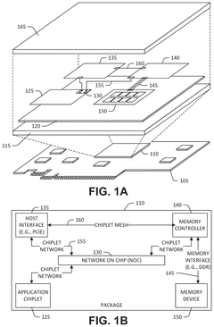
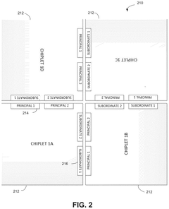
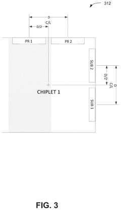
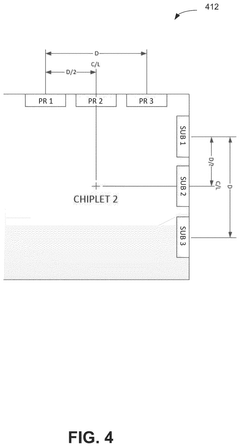
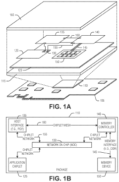
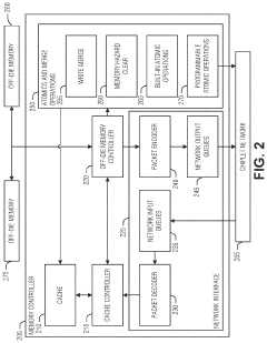
Edge interface placements to enable chiplet rotation into multi-chiplet cluster
PatentPendingUS20240332257A1
Innovation
- The implementation of a chiplet architecture that uses a network-on-chip (NOC) with a chiplet protocol interface (CPI) to facilitate high-speed, flexible inter-chiplet communication, combined with a tightly packed matrix arrangement of chiplets and I/O micro-bumps for close-coupled interconnects, allowing for proper alignment and minimal footprint.
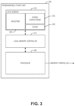
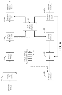
Rescheduling a failed memory request in a processor
PatentActiveUS12020064B2
Innovation
- The solution involves rescheduling threads that are denied memory requests as if the request was successful by placing them in an interim queue and using the existing memory response path, without additional circuitry, allowing hazards to be cleared without penalty to other threads.
Chiplet Standards
Chiplet standards play a crucial role in enabling interoperability and facilitating the integration of diverse chiplets from different vendors. These standards define common interfaces, protocols, and packaging technologies that allow chiplets to communicate and work together seamlessly within a single package. The development of chiplet standards has been driven by industry consortia and leading semiconductor companies to address the growing complexity and cost of chip design.
One of the most prominent chiplet standards is the Universal Chiplet Interconnect Express (UCIe), which was introduced in 2022. UCIe provides a standardized die-to-die interconnect that supports both package and silicon interoperability. This standard defines physical and protocol layers for both the die-to-die and package-to-package interfaces, enabling high-bandwidth, low-latency communication between chiplets.
Another important standard is the Advanced Interface Bus (AIB), developed by Intel. AIB focuses on providing a high-speed die-to-die PHY interface for chiplets, supporting data rates up to 2 Gbps per pin. This standard has been widely adopted and has evolved to include AIB 2.0, which offers improved performance and power efficiency.
The Open Compute Project (OCP) has also contributed to chiplet standardization efforts through its Open Domain-Specific Architecture (ODSA) subproject. The ODSA aims to develop open chiplet interfaces and foster an ecosystem of interoperable chiplets. Their work includes the development of the Bunch of Wires (BoW) interface, which provides a simple and cost-effective solution for chiplet-to-chiplet communication.
In addition to these standards, there are ongoing efforts to develop and refine chiplet standards for specific applications and industries. For example, the JEDEC Solid State Technology Association is working on standards for memory-centric chiplet architectures, while the Heterogeneous Integration Roadmap (HIR) is addressing broader challenges in chiplet integration across various domains.
As chiplet technology continues to evolve, these standards will play an increasingly important role in enabling best-in-class software integration. They provide a foundation for developers to create modular, scalable, and efficient chip designs that can leverage the strengths of different process nodes and specialized functionalities. The ongoing collaboration between industry leaders and standards organizations will be crucial in driving innovation and ensuring the widespread adoption of chiplet-based architectures in next-generation computing systems.
Chiplet Ecosystem
The Chiplet ecosystem has emerged as a transformative approach in semiconductor design and manufacturing, offering a paradigm shift in how complex integrated circuits are developed. This ecosystem encompasses a wide range of technologies, standards, and collaborations that enable the disaggregation of large monolithic chips into smaller, more manageable chiplets. These chiplets can be manufactured separately and then integrated onto a single package, allowing for greater flexibility, improved yield, and cost-effectiveness in chip production.
At the core of the Chiplet ecosystem are advanced packaging technologies that facilitate the interconnection of multiple chiplets. These include 2.5D and 3D packaging techniques, such as silicon interposers, through-silicon vias (TSVs), and advanced substrate technologies. These packaging innovations provide the foundation for high-bandwidth, low-latency communication between chiplets, enabling seamless integration and performance comparable to monolithic designs.
Standardization efforts play a crucial role in the Chiplet ecosystem's development. Industry consortia and organizations are working to establish common interfaces and protocols for chiplet-to-chiplet communication. Notable initiatives include the Universal Chiplet Interconnect Express (UCIe) and the Open Compute Project's Open Domain-Specific Architecture (ODSA). These standards aim to create a more open and interoperable ecosystem, allowing chiplets from different vendors to work together seamlessly.
The Chiplet ecosystem also encompasses design tools and methodologies tailored for multi-chiplet architectures. Electronic Design Automation (EDA) companies are developing specialized software to address the unique challenges of chiplet-based designs, including system-level optimization, thermal management, and signal integrity analysis across chiplet boundaries. These tools are essential for realizing the full potential of chiplet technology and enabling efficient design workflows.
Manufacturing and testing processes within the Chiplet ecosystem are evolving to meet the demands of multi-chiplet integration. Advanced foundries are developing specialized processes for chiplet fabrication and assembly, while test and validation methodologies are being adapted to ensure the reliability and performance of chiplet-based systems. This includes the development of known-good-die (KGD) testing techniques and advanced probe technologies for chiplet-level testing.
The ecosystem extends to include a diverse range of players, from semiconductor giants to specialized IP providers and packaging houses. Collaboration between these entities is driving innovation and fostering a rich ecosystem of chiplet offerings. This collaborative approach is enabling the creation of more customized and optimized solutions for various applications, from high-performance computing to edge AI devices.
As the Chiplet ecosystem continues to mature, it is poised to reshape the semiconductor industry landscape. The ability to mix and match chiplets from different vendors and process nodes opens up new possibilities for product differentiation and time-to-market advantages. This ecosystem approach is particularly valuable in addressing the challenges of Moore's Law scaling, offering a path forward for continued performance improvements and cost reductions in semiconductor design and manufacturing.
Unlock deeper insights with PatSnap Eureka Quick Research — get a full tech report to explore trends and direct your research. Try now!
Generate Your Research Report Instantly with AI Agent
Supercharge your innovation with PatSnap Eureka AI Agent Platform!