

How to Utilize Chiplet Architectures for Seamless Function Integration?
JUL 16, 20259 MIN READ
Generate Your Research Report Instantly with AI Agent
Patsnap Eureka helps you evaluate technical feasibility & market potential.
Chiplet Architecture Evolution and Objectives
Chiplet architecture has emerged as a revolutionary approach in semiconductor design, addressing the challenges of traditional monolithic integration. The evolution of chiplet technology can be traced back to the early 2010s when the semiconductor industry faced increasing difficulties in scaling down transistor sizes while maintaining performance and power efficiency. This paradigm shift was driven by the need to overcome the limitations of Moore's Law and the rising costs associated with advanced process nodes.
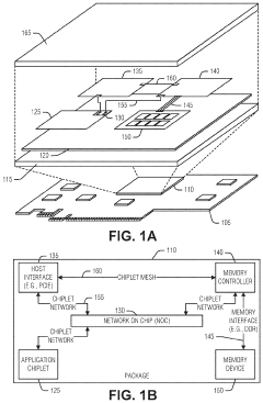
The primary objective of chiplet architecture is to enable seamless function integration by disaggregating complex system-on-chip (SoC) designs into smaller, more manageable components. This approach allows for the combination of different process technologies, intellectual property (IP) blocks, and functional units on a single package, offering unprecedented flexibility and cost-effectiveness in chip design.
As the technology evolved, several key milestones shaped its development. In 2015, AMD introduced its Infinity Fabric interconnect, laying the groundwork for chiplet-based designs. This was followed by the launch of AMD's Zen-based processors in 2017, which demonstrated the viability of chiplet architecture in high-performance computing. Intel joined the chiplet race with its Foveros 3D packaging technology in 2018, further advancing the field of heterogeneous integration.
The objectives of chiplet architecture extend beyond mere functional integration. They encompass improving yield rates by manufacturing smaller dies, reducing time-to-market for new products, and enabling more efficient use of advanced process nodes. Additionally, chiplet designs aim to enhance thermal management, optimize power consumption, and facilitate easier customization of chip configurations for specific applications.
Looking forward, the goals of chiplet architecture include standardization of interfaces and protocols to ensure interoperability between chiplets from different vendors. This standardization effort, led by initiatives such as the Universal Chiplet Interconnect Express (UCIe), seeks to create an ecosystem that fosters innovation and competition in the semiconductor industry.
Another critical objective is to push the boundaries of integration density and performance. Advanced packaging technologies like 2.5D and 3D integration are being developed to support higher bandwidth, lower latency interconnects between chiplets. These advancements aim to minimize the performance gap between chiplet-based designs and monolithic chips, while maintaining the flexibility and cost advantages of the chiplet approach.
Market Demand for Integrated Functionality
The market demand for integrated functionality in chiplet architectures is driven by the increasing complexity and performance requirements of modern electronic systems. As traditional monolithic chip designs reach their physical and economic limits, chiplet-based solutions offer a promising alternative to meet the growing need for seamless function integration across various industries.
In the consumer electronics sector, there is a strong demand for devices that combine multiple functionalities while maintaining compact form factors. Smartphones, tablets, and wearables require the integration of diverse components such as processors, memory, sensors, and communication modules. Chiplet architectures enable manufacturers to optimize each functional block independently and integrate them efficiently, resulting in improved performance, reduced power consumption, and enhanced user experiences.
The data center and cloud computing industry also exhibit a significant demand for integrated functionality. With the exponential growth of data processing and storage requirements, there is a need for high-performance, energy-efficient solutions that can handle complex workloads. Chiplet-based designs allow for the integration of specialized accelerators, memory subsystems, and networking components, enabling data centers to achieve higher computational density and improved overall system efficiency.
In the automotive sector, the trend towards advanced driver assistance systems (ADAS) and autonomous vehicles is driving the demand for highly integrated electronic systems. These applications require the seamless integration of sensors, processors, and communication modules to enable real-time decision-making and control. Chiplet architectures provide the flexibility to combine different functional blocks, such as radar, lidar, and vision processing units, into a single package, reducing system complexity and improving reliability.
The telecommunications industry, particularly with the rollout of 5G networks, is another area where integrated functionality is crucial. Base stations and network infrastructure equipment require the integration of multiple radio frequency (RF) components, digital signal processors, and high-speed interfaces. Chiplet-based designs offer the ability to optimize each functional block for specific frequency bands and performance requirements while maintaining overall system integration.
In the industrial and IoT sectors, there is a growing demand for edge computing solutions that can process data locally and reduce latency. Integrated functionality through chiplet architectures enables the combination of sensors, processors, and communication modules in compact form factors, suitable for deployment in various industrial environments and smart city applications.
The market demand for integrated functionality using chiplet architectures is expected to continue growing as industries seek more efficient, scalable, and cost-effective solutions to address their evolving technological needs. This trend is likely to drive innovation in chiplet design, packaging technologies, and integration methodologies to meet the diverse requirements of different market segments.
Current Challenges in Chiplet Integration
The integration of chiplets presents several significant challenges that need to be addressed for seamless function integration. One of the primary obstacles is the interconnect technology between chiplets. As chiplets are separate dies, the communication between them requires high-bandwidth, low-latency, and energy-efficient interconnects. Current solutions, such as silicon interposers and advanced packaging technologies, still face limitations in terms of bandwidth density and power efficiency.
Another critical challenge is thermal management. With multiple chiplets in close proximity, heat dissipation becomes more complex. The uneven heat distribution across different chiplets can lead to thermal hotspots, potentially causing performance degradation or reliability issues. Developing effective cooling solutions that can address the unique thermal characteristics of chiplet architectures is crucial.
Standardization is also a significant hurdle in chiplet integration. The lack of industry-wide standards for chiplet interfaces, protocols, and packaging makes it difficult for different manufacturers to create interoperable chiplets. This fragmentation hinders the development of a robust ecosystem and limits the potential for mix-and-match chiplet designs.
Power management poses another challenge in chiplet architectures. Coordinating power delivery and distribution across multiple chiplets requires sophisticated power management techniques. Ensuring efficient power delivery to each chiplet while maintaining overall system power efficiency is a complex task that demands innovative solutions.
Testing and validation of chiplet-based systems present unique challenges. Traditional testing methods may not be sufficient for verifying the functionality and performance of integrated chiplets. Developing new testing methodologies and tools that can effectively assess the interactions between chiplets and identify potential issues is essential for ensuring product quality and reliability.
The design and optimization of chiplet-based systems also face challenges in terms of system-level integration. Balancing the performance, power, and area trade-offs across multiple chiplets requires advanced design tools and methodologies. Additionally, optimizing the overall system architecture to leverage the benefits of chiplet integration while minimizing potential bottlenecks is a complex task that demands expertise in system-level design and optimization.
Lastly, manufacturing and yield management present challenges in chiplet integration. Ensuring consistent quality and yield across different chiplets, potentially from different manufacturing processes or even different foundries, requires sophisticated quality control measures and yield management strategies. Addressing these manufacturing challenges is crucial for the widespread adoption of chiplet architectures in high-volume production.
Existing Chiplet Integration Solutions
01 Modular chiplet architecture for function integration
Chiplet architectures allow for modular integration of different functional components on a single package. This approach enables the combination of various specialized chips, each optimized for specific functions, into a cohesive system. The modular design facilitates easier upgrades, customization, and potentially improved performance and power efficiency compared to monolithic designs.- Modular chiplet architecture for function integration: Chiplet architectures allow for modular integration of different functional components on a single package. This approach enables the combination of various specialized chips, each optimized for specific tasks, resulting in improved overall system performance and flexibility. The modular nature of chiplets facilitates easier upgrades and customization of semiconductor devices.
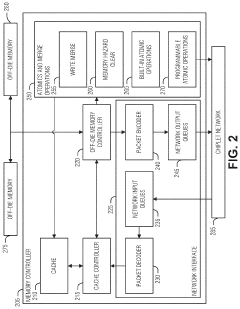
- Interconnect technologies for chiplet integration: Advanced interconnect technologies are crucial for efficient chiplet integration. These include high-bandwidth interfaces, through-silicon vias (TSVs), and interposers that enable seamless communication between different chiplets. Such interconnect solutions address challenges related to data transfer rates, power efficiency, and thermal management in multi-chiplet systems.
- Heterogeneous integration of chiplets: Heterogeneous integration involves combining chiplets manufactured using different process nodes or technologies. This approach allows for optimal performance-cost trade-offs by utilizing the most suitable manufacturing process for each functional block. It enables the integration of analog, digital, and mixed-signal components on a single package, enhancing overall system capabilities.
- Power management and thermal solutions for chiplet architectures: Effective power management and thermal solutions are essential for chiplet architectures. This includes advanced power delivery networks, dynamic power gating, and innovative cooling techniques to manage heat dissipation across multiple chiplets. These solutions ensure optimal performance and reliability of integrated chiplet systems under various operating conditions.
- Packaging technologies for chiplet integration: Advanced packaging technologies play a crucial role in chiplet integration. This includes 2.5D and 3D packaging techniques, as well as fan-out wafer-level packaging (FOWLP) that enable high-density interconnects between chiplets. These packaging solutions address challenges related to form factor, signal integrity, and thermal management in multi-chiplet systems.
02 Interconnect technologies for chiplet integration
Advanced interconnect technologies are crucial for efficient chiplet integration. These may include high-bandwidth interfaces, through-silicon vias (TSVs), and interposers to facilitate communication between chiplets. The choice of interconnect technology impacts the overall system performance, power consumption, and thermal management of the integrated chiplet architecture.Expand Specific Solutions03 Heterogeneous integration in chiplet designs
Chiplet architectures enable heterogeneous integration, allowing the combination of chips manufactured using different process nodes or even different materials. This approach can optimize cost and performance by using the most suitable technology for each functional block, while also potentially improving time-to-market for new products.Expand Specific Solutions04 Power management and thermal considerations in chiplet designs
Effective power management and thermal solutions are essential in chiplet architectures. This includes strategies for distributing power efficiently across multiple chiplets, managing heat dissipation, and optimizing performance based on thermal constraints. Advanced packaging techniques and cooling solutions may be employed to address these challenges in densely integrated chiplet systems.Expand Specific Solutions05 Software and system-level integration for chiplet architectures
Successful implementation of chiplet architectures requires sophisticated software and system-level integration. This includes developing efficient communication protocols between chiplets, optimizing data flow, and creating abstraction layers that allow seamless operation of the integrated system. Additionally, design tools and methodologies specific to chiplet-based systems are crucial for effective implementation and verification.Expand Specific Solutions
Key Players in Chiplet Ecosystem
The chiplet architecture market is in a growth phase, with increasing adoption across the semiconductor industry. Major players like Intel, AMD, and TSMC are investing heavily in this technology, driving market expansion. The global chiplet market size is projected to reach several billion dollars by 2025, with a compound annual growth rate exceeding 40%. Technologically, chiplet architectures are maturing rapidly, with advancements in integration techniques and interconnect technologies. Companies like Intel, AMD, and Micron are at the forefront, developing innovative chiplet designs for various applications. However, challenges remain in standardization and interoperability, indicating room for further technological progress and market development.
Intel Corp.
Technical Solution: Intel's chiplet architecture, known as "Foveros," utilizes 3D packaging technology to stack multiple chiplets vertically. This approach allows for the integration of diverse IP blocks and process nodes within a single package. Intel's Foveros technology enables the combination of high-performance compute tiles with low-power process technology tiles, optimizing both performance and power efficiency[1]. The company has implemented this architecture in products like Lakefield processors, which combine Core and Atom cores in a single package. Intel is also developing an advanced interconnect technology called EMIB (Embedded Multi-die Interconnect Bridge) to facilitate high-bandwidth, low-latency communication between chiplets[2].
Strengths: Vertical stacking allows for higher density and performance. Flexibility to mix and match different process nodes. Weaknesses: Potential thermal management challenges in 3D stacked designs. Higher manufacturing complexity and cost.
Huawei Technologies Co., Ltd.
Technical Solution: Huawei has been developing its own chiplet architecture, focusing on high-performance computing and AI applications. The company's approach involves creating a "chiplet-based ecosystem" that allows for the integration of various functional blocks from different vendors. Huawei's chiplet strategy emphasizes standardization of interfaces and protocols to enable seamless integration of diverse chiplets. The company has been working on advanced packaging technologies, including fan-out wafer-level packaging (FOWLP) and through-silicon vias (TSVs), to support high-density interconnects between chiplets[5]. Huawei has also been exploring the use of photonic interconnects for ultra-high-bandwidth communication between chiplets, potentially revolutionizing data transfer speeds within multi-chiplet systems[6].
Strengths: Focus on creating an open chiplet ecosystem. Exploration of advanced interconnect technologies. Weaknesses: Potential challenges in international collaboration due to geopolitical factors. Reliance on external foundries for advanced manufacturing processes.
Core Innovations in Chiplet Design
Method for configuring multiple input-output channels
PatentWO2022046284A1
Innovation
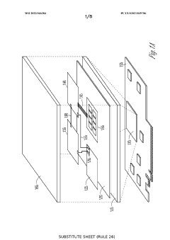
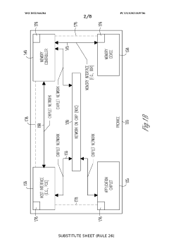
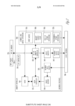
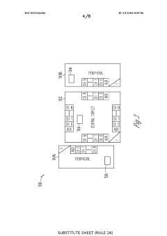
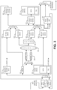
- The implementation of a Chiplet Protocol Interface (CPI) network with Advanced Interface Bus (AIB) channels and credit-based flow control, allowing for flexible virtual channel mapping and minimizing latency and energy consumption through packetized protocols and serialization-deserialization (SERDES) hardware, while enabling efficient inter-chiplet communication.
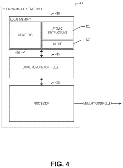
Communicating a programmable atomic operator to a memory controller
PatentPendingUS20230244416A1
Innovation
- A packet-based request and response technique is introduced to specify and invoke programmable atomic operators (PAOs) within a chiplet system, allowing for flexible and efficient invocation of PAOs by routing request packets through a packet-based network and decoding them to invoke the appropriate PAO, with responses transmitted back to the requesting process.
Standardization Efforts in Chiplet Technology
Standardization efforts in chiplet technology are crucial for enabling seamless function integration and promoting widespread adoption of chiplet architectures. These initiatives aim to establish common interfaces, protocols, and design methodologies that facilitate interoperability between chiplets from different manufacturers.
One of the most prominent standardization efforts is the Universal Chiplet Interconnect Express (UCIe) consortium. Launched in 2022, UCIe brings together industry leaders to develop an open interconnect standard for chiplets. The UCIe specification defines a die-to-die interconnect that enables high-bandwidth, low-latency communication between chiplets. This standard covers both the physical layer and the protocol layer, ensuring compatibility across different chiplet designs.
Another significant standardization initiative is the Open Compute Project's (OCP) Chiplet Design Exchange (CDX) format. CDX aims to create a common language for describing chiplet designs, enabling easier integration and collaboration between different chiplet providers. This format includes specifications for physical design, electrical characteristics, and thermal properties of chiplets.
The CHIPS Alliance, an open-source hardware initiative, is also contributing to chiplet standardization efforts. Their focus is on developing open-source tools and methodologies for chiplet-based system design. This includes work on interconnect protocols, design verification, and manufacturing test methodologies specific to chiplet architectures.
In addition to these industry-led efforts, government agencies are also supporting chiplet standardization. For example, the U.S. Department of Defense's CHIPS program (Common Heterogeneous Integration and IP Reuse Strategies) is funding research into standardized chiplet interfaces and integration methodologies for defense applications.
Standardization efforts also extend to packaging technologies that are critical for chiplet integration. The Joint Electron Device Engineering Council (JEDEC) is working on standards for advanced packaging technologies like 2.5D and 3D integration, which are essential for chiplet-based designs.
These standardization initiatives are essential for overcoming the challenges of chiplet integration, such as ensuring signal integrity across die-to-die interfaces, managing thermal issues in densely packed systems, and optimizing power delivery to multiple chiplets. By establishing common standards, the industry can reduce design complexity, improve time-to-market, and foster innovation in chiplet-based systems.
Thermal Management in Chiplet Designs
Thermal management is a critical aspect of chiplet designs, as the integration of multiple dies on a single package can lead to significant heat generation and distribution challenges. The compact nature of chiplet architectures often results in higher power densities, making efficient heat dissipation crucial for maintaining optimal performance and reliability.
One of the primary approaches to thermal management in chiplet designs is the implementation of advanced cooling solutions. These may include the use of high-performance thermal interface materials (TIMs) between the chiplets and the heat spreader, as well as the integration of sophisticated heat sinks and vapor chambers. Some designs incorporate liquid cooling systems or even immersion cooling for extreme thermal management requirements.
Another key strategy is the optimization of chiplet placement and interconnect design to facilitate better heat distribution. By carefully arranging chiplets based on their thermal characteristics and power consumption profiles, designers can minimize hotspots and create more uniform temperature gradients across the package. This may involve placing high-power chiplets closer to the edges of the package or interspersing them with lower-power components to improve overall thermal balance.
Advanced packaging technologies also play a crucial role in thermal management. For instance, the use of through-silicon vias (TSVs) and interposers can provide additional thermal pathways, allowing for more efficient heat dissipation from the chiplets to the package substrate and ultimately to the external environment. Some designs incorporate dedicated thermal TSVs or utilize the existing power and signal TSVs for dual-purpose heat conduction.
Power management techniques are integral to thermal control in chiplet architectures. Dynamic voltage and frequency scaling (DVFS) can be applied at the individual chiplet level, allowing for fine-grained control of power consumption and heat generation. Additionally, intelligent power gating and clock gating strategies can be employed to reduce power dissipation in inactive or lightly loaded chiplets.
Thermal sensing and management systems are often integrated into chiplet designs to provide real-time monitoring and adaptive control. These systems may include distributed temperature sensors across the package, along with sophisticated algorithms that can dynamically adjust power delivery, clock speeds, and cooling system parameters to maintain optimal thermal conditions under varying workloads.
As chiplet architectures continue to evolve, emerging technologies such as on-chip microfluidic cooling channels and phase-change materials for heat absorption are being explored to further enhance thermal management capabilities. These innovations promise to push the boundaries of chiplet integration and performance while maintaining strict thermal constraints.
Unlock deeper insights with Patsnap Eureka Quick Research — get a full tech report to explore trends and direct your research. Try now!
Generate Your Research Report Instantly with AI Agent
Supercharge your innovation with Patsnap Eureka AI Agent Platform!