Chiplet Technology and Its Role in Facilitating Digital Interactions
JUL 16, 20259 MIN READ
Generate Your Research Report Instantly with AI Agent
Patsnap Eureka helps you evaluate technical feasibility & market potential.
Chiplet Tech Evolution
Chiplet technology has undergone significant evolution since its inception, marking a paradigm shift in semiconductor design and manufacturing. The journey of chiplets began as a response to the challenges posed by Moore's Law, which was reaching its physical limits in traditional monolithic chip designs. As the industry faced increasing difficulties in scaling down transistors while maintaining performance and power efficiency, chiplets emerged as a promising solution.
The early stages of chiplet development focused on disaggregating large, complex System-on-Chip (SoC) designs into smaller, more manageable components. This approach allowed for better yield management and cost reduction by manufacturing different parts of a chip separately and then integrating them onto a single package. The initial implementations were primarily driven by the need to combine different process nodes or intellectual property (IP) blocks that were challenging to integrate monolithically.
As the technology matured, the industry witnessed a shift towards more standardized interfaces and packaging technologies. The development of advanced packaging solutions, such as 2.5D and 3D integration, played a crucial role in enabling efficient chiplet-based designs. These advancements allowed for higher bandwidth, lower latency, and improved power efficiency in inter-chiplet communications.
The evolution of chiplet technology also saw the emergence of various interconnect standards and protocols. Industry collaborations led to the development of open standards like Universal Chiplet Interconnect Express (UCIe), which aimed to create a common ecosystem for chiplet-based designs across different manufacturers. This standardization effort has been instrumental in fostering innovation and reducing barriers to entry for smaller players in the semiconductor industry.
Recent years have seen a significant focus on enhancing the integration density and performance of chiplet-based systems. Advanced packaging technologies like silicon interposers and through-silicon vias (TSVs) have enabled tighter integration of chiplets, leading to performance levels that rival or exceed monolithic designs. The industry has also witnessed the development of active interposers, which incorporate additional functionality to further optimize system-level performance and power efficiency.
The role of chiplets in facilitating digital interactions has become increasingly prominent as the technology has evolved. By enabling more powerful and efficient computing systems, chiplets have contributed to advancements in areas such as artificial intelligence, high-performance computing, and edge computing. These technologies, in turn, have driven innovations in digital communication, data processing, and user interfaces, enhancing the overall digital interaction experience.
Looking ahead, the evolution of chiplet technology is expected to continue, with a focus on further miniaturization, improved energy efficiency, and enhanced integration capabilities. As the technology matures, it is likely to play an even more significant role in shaping the future of digital interactions, enabling more sophisticated and seamless experiences across a wide range of applications and devices.
Digital Interaction Needs
The digital landscape is rapidly evolving, driven by the increasing demand for more sophisticated and seamless digital interactions. As our world becomes increasingly interconnected, the need for advanced technologies that can facilitate these interactions has become paramount. Chiplet technology has emerged as a promising solution to meet these growing demands, offering enhanced performance, scalability, and efficiency in digital systems.
The primary digital interaction needs that chiplet technology aims to address include faster data processing, improved energy efficiency, and enhanced connectivity. In today's data-driven world, users expect instantaneous responses and real-time interactions across various digital platforms. This requires powerful computing capabilities that can handle complex algorithms and process vast amounts of data quickly. Chiplet technology, with its modular approach to chip design, allows for the integration of specialized processing units that can be optimized for specific tasks, thereby significantly boosting overall system performance.
Energy efficiency is another critical factor in digital interactions, particularly as mobile devices and edge computing continue to proliferate. Users demand longer battery life and reduced power consumption without compromising on performance. Chiplet technology offers a solution by allowing for more efficient power management through the integration of purpose-built components that can be selectively activated based on the specific requirements of a given task.
Connectivity is at the heart of digital interactions, and the need for seamless, high-bandwidth communication between devices and systems is ever-increasing. Chiplet technology facilitates this by enabling the integration of advanced communication interfaces and protocols directly into the chip design. This allows for faster data transfer rates and more robust connections between different components of a digital ecosystem.
As augmented reality (AR), virtual reality (VR), and artificial intelligence (AI) applications become more prevalent, the demand for more powerful and efficient computing solutions grows. Chiplet technology is well-positioned to meet these needs by providing the flexibility to combine different types of processing units, memory modules, and specialized accelerators on a single package. This heterogeneous integration allows for the creation of highly customized solutions that can deliver the performance required for immersive AR/VR experiences and complex AI computations.
Furthermore, the Internet of Things (IoT) ecosystem continues to expand, creating a need for chips that can operate efficiently in a wide range of devices, from small sensors to edge computing nodes. Chiplet technology's modular nature allows for the development of scalable solutions that can be adapted to various IoT applications, balancing performance, power consumption, and cost considerations.
In conclusion, the digital interaction needs driving the development of chiplet technology are multifaceted, encompassing performance, efficiency, connectivity, and adaptability. As these needs continue to evolve, chiplet technology stands poised to play a crucial role in shaping the future of digital interactions, enabling more immersive, responsive, and intelligent digital experiences across a wide spectrum of applications and devices.
Chiplet Challenges
Despite the promising potential of chiplet technology, several significant challenges need to be addressed for its widespread adoption and successful implementation in facilitating digital interactions. One of the primary obstacles is the complexity of integration. Chiplets require sophisticated packaging techniques and interconnect technologies to function as a cohesive unit. This integration process demands advanced manufacturing capabilities and expertise, which may not be readily available to all semiconductor companies.
Another critical challenge lies in the standardization of chiplet interfaces. The lack of universal standards for chiplet-to-chiplet communication and integration can hinder interoperability between chiplets from different manufacturers. This absence of standardization may lead to increased design complexity and potential compatibility issues, limiting the flexibility and scalability of chiplet-based solutions.
Thermal management presents a significant hurdle in chiplet design. As multiple chiplets are integrated into a single package, heat dissipation becomes more complex. Efficient cooling solutions must be developed to ensure optimal performance and reliability of chiplet-based systems, particularly in high-performance computing applications where thermal constraints are critical.
The testing and validation of chiplet-based systems pose unique challenges. Traditional testing methods may not be sufficient to ensure the functionality and performance of integrated chiplets. New testing methodologies and equipment need to be developed to address the specific requirements of chiplet technology, potentially increasing development time and costs.
Supply chain management and logistics also present challenges in the chiplet ecosystem. Coordinating the production and assembly of multiple chiplets from various suppliers requires sophisticated supply chain strategies. Ensuring consistent quality, timely delivery, and seamless integration of chiplets from different sources can be complex and may introduce new risks to the manufacturing process.
Furthermore, the economic viability of chiplet technology remains a concern. While chiplets offer potential cost savings in certain scenarios, the initial investment in research, development, and manufacturing infrastructure can be substantial. Companies must carefully evaluate the long-term cost-benefit analysis of adopting chiplet technology, considering factors such as yield improvements, design flexibility, and time-to-market advantages.
Lastly, intellectual property (IP) management and protection present challenges in the chiplet ecosystem. As chiplet designs may involve collaboration between multiple parties, clear IP agreements and licensing models need to be established to protect innovations and foster a healthy chiplet marketplace. Balancing open collaboration with proprietary technology protection will be crucial for the sustainable growth of the chiplet industry.
Current Chiplet Solutions
01 Chiplet integration and packaging
Chiplet technology involves integrating multiple smaller chips (chiplets) into a single package. This approach allows for more flexible and efficient chip design, enabling the combination of different functionalities and manufacturing processes. Advanced packaging techniques are used to connect and assemble these chiplets, improving overall system performance and reducing costs.- Chiplet integration and packaging: Chiplet technology involves integrating multiple smaller chips (chiplets) into a single package. This approach allows for more flexible and efficient chip design, enabling the combination of different process nodes and functionalities. Advanced packaging techniques are used to connect these chiplets, improving overall system performance and reducing costs.
- Interconnect technologies for chiplets: Various interconnect technologies are employed to facilitate communication between chiplets within a package. These may include advanced interposers, silicon bridges, or through-silicon vias (TSVs). The choice of interconnect technology impacts the bandwidth, latency, and power efficiency of the overall chiplet-based system.
- Thermal management in chiplet designs: Effective thermal management is crucial in chiplet-based systems due to the high density of components. Innovative cooling solutions and thermal interface materials are developed to address heat dissipation challenges, ensuring optimal performance and reliability of the integrated chiplets.
- Power distribution and management for chiplets: Efficient power distribution and management are essential in chiplet designs to optimize performance and reduce energy consumption. Advanced power delivery networks and voltage regulation techniques are implemented to ensure stable power supply across multiple chiplets with varying power requirements.
- Design and verification tools for chiplet-based systems: Specialized design and verification tools are developed to address the unique challenges of chiplet-based systems. These tools facilitate the integration of multiple chiplets, optimize system-level performance, and ensure compatibility between different chiplets from various vendors or process nodes.
02 Interconnect technologies for chiplets
Various interconnect technologies are crucial for chiplet-based designs. These include advanced die-to-die interfaces, high-bandwidth connections, and novel packaging solutions. Such technologies enable efficient communication between chiplets, reducing latency and power consumption while increasing data transfer rates.Expand Specific Solutions03 Thermal management in chiplet designs
Effective thermal management is essential in chiplet-based systems due to the high density of components. Innovative cooling solutions, heat spreading techniques, and thermal-aware designs are employed to maintain optimal operating temperatures and ensure reliability of the integrated chiplets.Expand Specific Solutions04 Power distribution and management for chiplets
Efficient power distribution and management are critical in chiplet-based designs. This includes developing advanced power delivery networks, implementing fine-grained power control mechanisms, and optimizing power consumption across different chiplets to enhance overall system efficiency and performance.Expand Specific Solutions05 Design and verification methodologies for chiplet-based systems
Developing robust design and verification methodologies is crucial for chiplet-based systems. This includes creating new EDA tools, establishing standards for chiplet interfaces, and implementing comprehensive testing strategies to ensure the reliability and functionality of complex multi-chiplet designs.Expand Specific Solutions
Key Chiplet Players
The chiplet technology market is in a growth phase, with increasing adoption across the semiconductor industry. The market size is expanding rapidly, driven by demand for more efficient and scalable chip designs. Technological maturity varies, with leading companies like Intel, AMD, and TSMC at the forefront of development. Micron Technology and Huawei are also making significant strides in chiplet integration. Emerging players such as Hygon and Moore Thread are contributing to the competitive landscape. While still evolving, chiplet technology is gaining traction in high-performance computing, data centers, and AI applications, indicating a promising future for digital interactions facilitated by this innovative approach to chip design.
Huawei Technologies Co., Ltd.
Technical Solution: Huawei has been at the forefront of chiplet technology research, developing their Kirin 9000 SoC using chiplet architecture. Their approach involves integrating multiple dies on a single package, including CPU, GPU, and AI processors. Huawei's chiplet design allows for improved performance and power efficiency by optimizing each component separately. They have implemented advanced packaging technologies such as Chip-on-Wafer-on-Substrate (CoWoS) to enable high-bandwidth interconnects between chiplets[1]. Huawei's chiplet strategy also focuses on heterogeneous integration, combining different process nodes to balance performance and cost[2].
Strengths: Advanced packaging technology, heterogeneous integration capabilities, and improved performance-to-power ratio. Weaknesses: Potential supply chain vulnerabilities due to geopolitical issues, and increased complexity in design and manufacturing processes.
Intel Corp.
Technical Solution: Intel has been a pioneer in chiplet technology with their Foveros 3D packaging technology. This approach allows for vertical stacking of chiplets, enabling higher performance and lower power consumption. Intel's Lakefield processors were among the first to use this technology commercially. Their latest advancements include Foveros Omni and Foveros Direct, which offer even more flexibility in chiplet integration[3]. Intel's chiplet strategy also includes their EMIB (Embedded Multi-die Interconnect Bridge) technology, which provides high-bandwidth connections between chiplets in a 2.5D configuration[4]. Intel is also working on standardizing chiplet interfaces through their Universal Chiplet Interconnect Express (UCIe) initiative, aiming to create an open ecosystem for chiplet-based designs[5].
Strengths: Advanced 3D packaging technologies, established manufacturing capabilities, and efforts towards standardization. Weaknesses: Historically slower adoption of new technologies compared to competitors, and potential challenges in maintaining leadership in a rapidly evolving field.
Chiplet Innovations
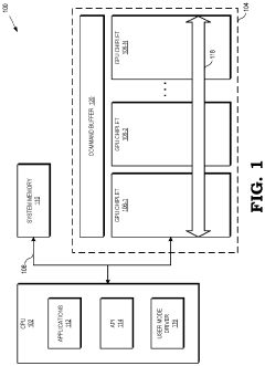
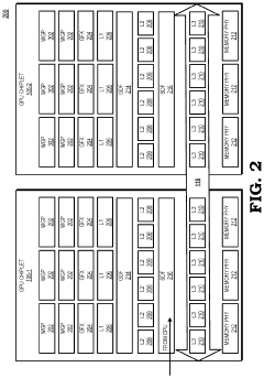
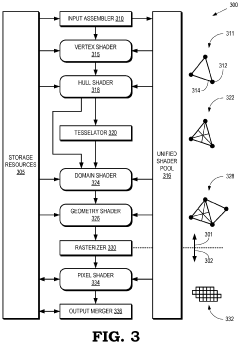
Data flow in a distributed graphics processing unit architecture
PatentActiveUS20210158599A1
Innovation
- A distributed architecture using chiplets with high-performance interconnection, where geometry and pixel workloads are processed by multiple processing units with duplicated fixed function hardware blocks and shaders, and a shared coherent cache, allowing for checkerboarding of pixel processing across units to manage synchronization and bandwidth effectively.
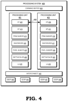
Assembly having a face-to-face bonded chiplet
PatentWO2025042587A1
Innovation
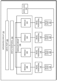
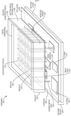
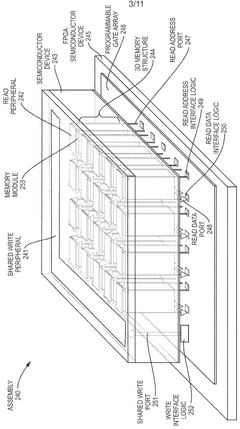
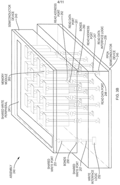
- The proposed integrated circuit architecture features a face-to-face bonded chiplet configuration, incorporating a shared write port and multiple read ports, along with a network-on-chip fabric, to enable efficient communication and data management across multiple semiconductor devices.
Chiplet Ecosystem
The chiplet ecosystem is rapidly evolving, driven by the need for more efficient and scalable semiconductor solutions. This ecosystem encompasses a wide range of players, including chip designers, manufacturers, packaging companies, and tool providers. At its core, the chiplet approach allows for the disaggregation of complex system-on-chip (SoC) designs into smaller, more manageable components.
Key players in the chiplet ecosystem include major semiconductor companies like Intel, AMD, and TSMC, as well as specialized firms focusing on advanced packaging technologies. These companies are investing heavily in research and development to overcome the challenges associated with chiplet integration, such as high-speed interconnects and thermal management.
The ecosystem is supported by a growing number of industry standards and initiatives. The Universal Chiplet Interconnect Express (UCIe) consortium, for example, is working to establish a common interconnect standard for chiplets, enabling interoperability between different vendors' components. This standardization effort is crucial for fostering innovation and competition within the ecosystem.
Packaging technologies play a critical role in the chiplet ecosystem. Advanced packaging techniques like 2.5D and 3D integration are enabling the creation of complex multi-chip modules that combine chiplets from different process nodes and even different manufacturers. This flexibility is driving new business models and partnerships within the semiconductor industry.
The chiplet ecosystem is also spurring innovation in design tools and methodologies. Electronic design automation (EDA) companies are developing new software solutions to address the unique challenges of chiplet-based designs, including system-level optimization and die-to-die interface planning.
As the ecosystem matures, we are seeing the emergence of specialized chiplet marketplaces and platforms. These platforms aim to facilitate the exchange of chiplet designs and intellectual property, potentially democratizing access to advanced semiconductor capabilities for smaller companies and startups.
The growth of the chiplet ecosystem is having far-reaching implications for the semiconductor supply chain. It is enabling a more modular and flexible approach to chip design and manufacturing, potentially reducing development costs and time-to-market for new products. This shift is particularly significant in the context of facilitating digital interactions, as it allows for the rapid development of customized solutions for emerging applications in areas such as artificial intelligence, edge computing, and 5G communications.
Chiplet Standardization
Chiplet standardization is a critical aspect of the evolving chiplet technology landscape, playing a pivotal role in facilitating digital interactions and enabling the widespread adoption of this innovative approach to semiconductor design. As the industry moves towards more modular and flexible chip architectures, the need for standardized interfaces and protocols becomes increasingly apparent.
The primary goal of chiplet standardization is to establish a common framework that allows seamless integration of diverse chiplets from different manufacturers. This standardization effort encompasses various aspects, including physical interconnects, communication protocols, and power management interfaces. By creating a unified set of standards, the industry aims to reduce design complexity, improve interoperability, and accelerate time-to-market for chiplet-based products.
One of the key initiatives driving chiplet standardization is the Universal Chiplet Interconnect Express (UCIe) consortium. Formed by leading semiconductor companies, UCIe focuses on developing open specifications for die-to-die interconnects. These specifications cover both the physical layer and the protocol layer, ensuring consistent communication between chiplets regardless of their origin or manufacturer.
Another significant standardization effort is the Open Compute Project's (OCP) Chiplet Design Exchange (CDX) format. CDX aims to create a standardized way of describing chiplet designs, facilitating easier exchange of chiplet intellectual property (IP) between different parties. This standardization of design information is crucial for enabling a more open and collaborative chiplet ecosystem.
The Advanced Packaging Collective (AP Collective) is also contributing to chiplet standardization by focusing on advanced packaging technologies. Their work includes developing standards for chiplet-to-substrate connections and thermal management, which are essential for realizing the full potential of chiplet-based designs.
Standardization efforts extend to software interfaces as well. The CHIPS Alliance, for instance, is working on standardizing software-hardware interfaces for chiplets, ensuring that operating systems and applications can effectively utilize the capabilities of diverse chiplet configurations.
As chiplet standardization progresses, it faces several challenges. One of the primary hurdles is balancing the need for standardization with the desire for innovation and differentiation among chiplet manufacturers. Finding the right level of standardization that promotes interoperability without stifling creativity is a delicate balance that industry consortia must navigate.
Looking ahead, the success of chiplet standardization will be crucial in shaping the future of semiconductor design and digital interactions. As standards mature and gain widespread adoption, we can expect to see a more diverse and competitive chiplet ecosystem emerge, leading to more innovative and cost-effective solutions across a wide range of applications.
Unlock deeper insights with Patsnap Eureka Quick Research — get a full tech report to explore trends and direct your research. Try now!
Generate Your Research Report Instantly with AI Agent
Supercharge your innovation with Patsnap Eureka AI Agent Platform!