

How to Achieve Cost Reduction Through Chiplet-Driven Solutions?
JUL 16, 20259 MIN READ
Generate Your Research Report Instantly with AI Agent
Patsnap Eureka helps you evaluate technical feasibility & market potential.
Chiplet Technology Evolution and Cost Reduction Goals
Chiplet technology has emerged as a revolutionary approach in semiconductor design and manufacturing, offering a pathway to overcome the limitations of traditional monolithic chip designs. The evolution of chiplet technology can be traced back to the early 2010s when the semiconductor industry began facing challenges in scaling down transistor sizes while maintaining performance improvements and cost-effectiveness. This led to the exploration of alternative architectures, ultimately giving rise to the chiplet concept.
The primary goal of chiplet technology is to achieve cost reduction while maintaining or improving performance and functionality. This is accomplished by breaking down complex system-on-chip (SoC) designs into smaller, modular components called chiplets. These chiplets can be manufactured using different process nodes, allowing for optimal cost-performance trade-offs for each component. The evolution of chiplet technology has been driven by the need to address several key challenges in the semiconductor industry.
One of the main drivers for chiplet adoption has been the increasing costs associated with advanced process nodes. As the industry moves towards smaller transistor sizes, the cost of designing and manufacturing chips at these nodes has grown exponentially. Chiplet technology allows companies to leverage older, more cost-effective process nodes for certain components while using advanced nodes only where necessary. This selective use of advanced processes helps in managing overall costs while still delivering high-performance solutions.
Another significant factor in the evolution of chiplet technology has been the demand for more specialized and diverse computing solutions. As different applications require varying levels of performance and functionality, chiplet-based designs offer greater flexibility in creating customized solutions. This modular approach allows for faster time-to-market and reduced development costs, as chiplets can be mixed and matched to create new products without redesigning entire systems from scratch.
The cost reduction goals associated with chiplet technology are multifaceted. Firstly, by enabling the use of older process nodes for certain components, chiplet designs can significantly reduce manufacturing costs. Secondly, the modular nature of chiplets allows for better yield management, as smaller dies are less prone to defects compared to large monolithic chips. This improved yield translates directly into cost savings. Additionally, chiplet technology enables more efficient use of silicon area, reducing waste and further contributing to cost reduction.
As the technology continues to evolve, industry standards and ecosystems are being developed to facilitate interoperability between chiplets from different manufacturers. This standardization effort aims to create a more open and competitive market for chiplet-based solutions, potentially leading to further cost reductions through increased competition and economies of scale. The future of chiplet technology lies in refining integration techniques, improving inter-chiplet communication, and expanding the range of applications where chiplet-based designs can offer significant cost and performance benefits.
Market Demand for Cost-Effective Semiconductor Solutions
The semiconductor industry is experiencing a growing demand for cost-effective solutions, driven by the increasing complexity and cost of chip manufacturing. As traditional Moore's Law scaling becomes more challenging and expensive, chiplet-based designs have emerged as a promising approach to achieve cost reduction while maintaining performance improvements.
Market research indicates that the global semiconductor industry is projected to reach $1 trillion by 2030, with a significant portion of this growth attributed to advanced packaging technologies, including chiplets. The demand for cost-effective semiconductor solutions is particularly strong in high-performance computing, data centers, and consumer electronics sectors, where the need for powerful yet affordable chips is paramount.
Chiplet-driven solutions offer several advantages that align with market demands. Firstly, they allow for the disaggregation of complex system-on-chip (SoC) designs into smaller, more manageable components. This modular approach enables manufacturers to mix and match different process nodes, optimizing cost and performance for specific functions within a single package.
The market is also showing increased interest in chiplet solutions due to their potential for improved yield and reduced waste. By fabricating smaller dies, manufacturers can achieve higher yields, as the probability of defects decreases with smaller chip sizes. This translates to lower production costs and improved overall efficiency, addressing the market's need for more cost-effective semiconductor products.
Furthermore, the flexibility offered by chiplet designs allows for faster time-to-market and easier product customization. This is particularly valuable in rapidly evolving markets such as artificial intelligence and 5G, where the ability to quickly adapt and iterate on designs is crucial for maintaining competitiveness.
The demand for chiplet-based solutions is also driven by the need for more energy-efficient computing. As data centers and edge computing applications continue to grow, there is a pressing requirement for chips that can deliver high performance while minimizing power consumption. Chiplet architectures enable more efficient power distribution and thermal management, aligning with the market's focus on sustainability and reduced operational costs.
In the consumer electronics sector, the demand for more powerful yet affordable devices is pushing manufacturers to explore chiplet solutions. This approach allows for the integration of high-performance components with more cost-effective elements, enabling the creation of feature-rich products at competitive price points.
As the semiconductor industry continues to evolve, the market demand for cost-effective solutions through chiplet-driven approaches is expected to grow significantly. This trend is likely to shape the future of chip design and manufacturing, driving innovation in packaging technologies and fostering collaboration across the semiconductor ecosystem.
Current Challenges in Chiplet-Based Cost Reduction
While chiplet-based solutions offer significant potential for cost reduction in semiconductor manufacturing, several challenges currently impede their widespread adoption and full realization of cost benefits. One of the primary obstacles is the lack of standardization in chiplet interfaces and packaging technologies. This absence of industry-wide standards creates compatibility issues between chiplets from different manufacturers, limiting the flexibility and interoperability of chiplet-based designs.
Another significant challenge lies in the complexity of system integration. Chiplet-based designs require intricate interconnects and advanced packaging technologies, which can increase manufacturing complexity and potentially offset some of the cost savings. The need for high-bandwidth, low-latency connections between chiplets also presents technical hurdles that must be overcome to ensure optimal performance.
Thermal management poses another critical challenge in chiplet-based solutions. As multiple chiplets are integrated into a single package, managing heat dissipation becomes more complex. Ineffective thermal solutions can lead to performance degradation and reliability issues, potentially increasing long-term costs.
The testing and validation of chiplet-based systems present additional challenges. Traditional testing methods may not be sufficient for assessing the performance and reliability of interconnected chiplets, necessitating the development of new testing protocols and equipment. This can increase development time and costs in the short term.
Supply chain management also becomes more complex with chiplet-based solutions. Coordinating the production and assembly of multiple chiplets from potentially different suppliers requires sophisticated logistics and quality control measures. Any disruption in the supply chain can have cascading effects on production schedules and costs.
Intellectual property (IP) management and licensing present legal and business challenges in the chiplet ecosystem. As different companies may own the IP for various chiplets, negotiating licensing agreements and ensuring fair compensation for all parties involved can be complex and potentially increase overall costs.
Lastly, the initial investment required for transitioning to chiplet-based manufacturing can be substantial. This includes costs associated with redesigning existing products, acquiring new manufacturing equipment, and training personnel. While these investments may lead to long-term cost savings, they can present significant financial barriers, especially for smaller companies or those with limited resources.
Existing Chiplet-Based Cost Reduction Strategies
01 Cost reduction through modular design
Chiplet-driven solutions enable cost reduction through modular design, allowing for the use of smaller, more specialized chips that can be combined to create complex systems. This approach reduces manufacturing costs by improving yield rates and allowing for the reuse of proven designs across multiple products.- Cost reduction through modular design: Chiplet-driven solutions enable cost reduction through modular design. By breaking down complex systems into smaller, reusable components, manufacturers can achieve economies of scale and reduce production costs. This approach allows for more efficient use of silicon area and enables the mixing of different process nodes, further optimizing costs.
- Improved yield and defect management: Chiplet technology improves yield and defect management in semiconductor manufacturing. By producing smaller chiplets instead of large monolithic dies, the probability of defects is reduced, leading to higher yields and lower costs. This approach also allows for easier isolation and replacement of faulty components, reducing overall production expenses.
- Flexible manufacturing and customization: Chiplet-driven solutions offer flexible manufacturing and customization options, potentially reducing costs. Manufacturers can mix and match chiplets to create various product configurations, allowing for more efficient inventory management and reduced time-to-market. This flexibility also enables easier product updates and customization without redesigning entire systems.
- Advanced packaging technologies: The adoption of advanced packaging technologies in chiplet-based designs can lead to cost savings. These technologies, such as 2.5D and 3D integration, allow for higher density and performance while potentially reducing overall system costs. Improved thermal management and power efficiency in these packaging solutions can also contribute to long-term cost savings.
- Supply chain optimization: Chiplet-driven solutions can optimize the semiconductor supply chain, potentially reducing costs. By allowing different components to be sourced from various suppliers and manufactured using different processes, companies can leverage competitive pricing and reduce dependency on single sources. This approach can also lead to more resilient supply chains and potentially lower overall production costs.
02 Improved manufacturing efficiency
Chiplet solutions improve manufacturing efficiency by allowing parallel production of different components. This approach reduces overall production time and costs, as individual chiplets can be manufactured using optimal processes for each specific technology node, leading to higher yields and lower defect rates.Expand Specific Solutions03 Flexible integration and scalability
Chiplet-driven solutions offer flexible integration and scalability, allowing manufacturers to mix and match different chiplets to create customized products. This flexibility reduces development costs and time-to-market for new products, as existing chiplet designs can be reused and combined in novel ways to meet specific performance and cost requirements.Expand Specific Solutions04 Advanced packaging technologies
The adoption of advanced packaging technologies, such as 2.5D and 3D integration, enables more efficient chiplet interconnections. These packaging solutions reduce overall system costs by improving power efficiency, reducing form factors, and enabling higher performance without the need for monolithic chip designs.Expand Specific Solutions05 Ecosystem and standardization efforts
The development of chiplet ecosystems and standardization efforts contribute to cost reduction by promoting interoperability and reducing design complexity. Standardized interfaces and protocols enable chiplets from different vendors to work together seamlessly, fostering competition and driving down costs across the industry.Expand Specific Solutions
Key Players in Chiplet-Driven Solutions
The chiplet-driven solutions market is in its early growth stage, with increasing adoption across the semiconductor industry. The market size is expanding rapidly, driven by the need for cost-effective and scalable chip designs. Technological maturity varies among key players, with companies like AMD, Intel, and Micron Technology leading in chiplet implementation. Advanced Micro Devices has made significant strides with its chiplet-based processors, while Intel is developing its own chiplet technologies. Emerging players such as Primemas and AvicenaTech are focusing on innovative chiplet interconnect solutions. The competitive landscape is dynamic, with both established semiconductor giants and specialized startups vying for market share in this promising field.
Advanced Micro Devices, Inc.
Technical Solution: AMD's chiplet-driven solution revolves around their Infinity Fabric interconnect technology and chiplet-based design approach. The company has successfully implemented chiplets in their Ryzen CPUs and EPYC server processors, demonstrating significant cost reductions. AMD's approach involves manufacturing smaller, more uniform chiplets on advanced process nodes and connecting them using their high-bandwidth, low-latency Infinity Fabric[4]. This strategy allows AMD to achieve higher yields, as smaller dies are less prone to defects, and enables the company to mix and match chiplets with different functionalities. AMD has reported up to 41% cost reduction per wafer through their chiplet approach compared to monolithic designs[5]. The company has also extended this technology to their GPUs, with the RDNA 3 architecture incorporating chiplet designs for further cost optimization and performance improvements[6].
Strengths: Higher yields due to smaller die sizes. Flexibility in product configurations. Cost-effective scaling of performance. Weaknesses: Potential latency overhead in inter-chiplet communication. Complexity in system integration and packaging.
Intel Corp.
Technical Solution: Intel's chiplet-driven solution focuses on their Foveros 3D packaging technology. This approach allows for the vertical stacking of multiple chiplets, enabling the integration of diverse IP blocks and process nodes in a single package. Intel's Foveros technology utilizes through-silicon vias (TSVs) and micro-bumps to connect different layers, allowing for high-bandwidth, low-latency communication between chiplets[1]. The company has demonstrated cost reduction through their disaggregated design approach, which allows for the mixing and matching of different process nodes for various components, optimizing performance and cost[2]. Intel's Ponte Vecchio GPU, built using Foveros, incorporates over 40 chiplets manufactured on different process nodes, showcasing the scalability and flexibility of their chiplet solution[3].
Strengths: Vertical stacking allows for higher density and performance. Flexibility in mixing different process nodes. Weaknesses: Complex manufacturing process may impact yields. Thermal management challenges in 3D stacked designs.
Core Innovations in Chiplet Integration Technologies
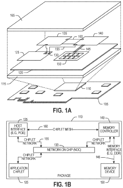
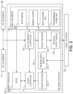
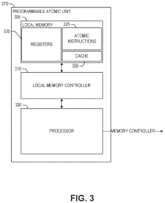
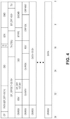
Method of executing programmable atomic unit resources within a multi-process system
PatentActiveUS12020062B2
Innovation
- A method is disclosed that involves determining a unique identifier for a programmable atomic transaction within a process, using a mapping table to generate a system-wide identifier, and issuing requests to a memory controller to perform the transaction, allowing for efficient execution and response handling through a programmable atomic unit.
Supply Chain Implications of Chiplet Adoption
The adoption of chiplet technology is poised to significantly reshape the semiconductor supply chain, introducing both opportunities and challenges for industry players. As chiplet-based solutions gain traction, the traditional monolithic chip production model is evolving towards a more modular and flexible approach, necessitating adaptations across the entire supply chain.
One of the primary implications of chiplet adoption is the potential for increased specialization among suppliers. With chiplets allowing for the disaggregation of chip components, different manufacturers can focus on producing specific types of chiplets, leveraging their core competencies. This specialization can lead to improved efficiency and cost-effectiveness in the production process, as suppliers can optimize their manufacturing processes for specific chiplet types.
The modular nature of chiplets also introduces new possibilities for supply chain diversification. Companies can source different chiplets from multiple suppliers, reducing dependency on a single source and potentially mitigating supply chain risks. This diversification can enhance resilience against disruptions and provide more flexibility in managing supply chain relationships.
However, the transition to chiplet-based solutions also presents challenges for supply chain management. The increased complexity of integrating multiple chiplets from various sources requires more sophisticated logistics and quality control processes. Ensuring compatibility and performance consistency across chiplets from different suppliers becomes crucial, necessitating robust testing and validation procedures throughout the supply chain.
The adoption of chiplets may also lead to shifts in the geographical distribution of semiconductor manufacturing. As different regions specialize in producing specific types of chiplets, new manufacturing hubs may emerge, potentially altering existing supply chain dynamics and trade flows.
Furthermore, the chiplet approach may impact inventory management strategies. The ability to mix and match chiplets for different end products could lead to more flexible inventory practices, potentially reducing overall inventory costs. However, it may also require more sophisticated forecasting and demand planning to ensure the availability of the right chiplet combinations.
The transition to chiplet-based solutions also has implications for packaging and assembly processes within the supply chain. Advanced packaging technologies become increasingly critical, as the integration of multiple chiplets requires sophisticated interconnect solutions. This shift may lead to the emergence of new specialized players in the packaging and assembly segment of the supply chain.
In conclusion, the adoption of chiplet technology is set to bring about significant changes in the semiconductor supply chain, offering opportunities for cost reduction and increased flexibility, while also introducing new complexities and challenges that industry participants must navigate.
Standardization Efforts in Chiplet Ecosystems
Standardization efforts in chiplet ecosystems are crucial for achieving cost reduction through chiplet-driven solutions. As the semiconductor industry increasingly adopts chiplet-based designs, the need for common standards and interfaces becomes paramount to ensure interoperability and reduce integration complexities.
One of the most significant standardization initiatives is the Universal Chiplet Interconnect Express (UCIe), which aims to establish a unified die-to-die interconnect standard. UCIe provides a common physical and protocol layer specification, enabling chiplets from different vendors to communicate seamlessly. This standardization effort is backed by major industry players, including Intel, AMD, Arm, and TSMC, highlighting its potential to become a widely adopted standard.
Another important standardization effort is the Open Compute Project's (OCP) Chiplet Design Exchange (CDX) format. CDX aims to create a standardized way of describing chiplet designs, facilitating easier exchange of chiplet intellectual property (IP) between different companies. This standardization can significantly reduce the time and cost associated with chiplet integration and verification.
The CHIPS Alliance, an open-source hardware initiative, is also contributing to chiplet standardization efforts. Their work focuses on developing open-source tools and methodologies for chiplet-based designs, which can help reduce the barriers to entry for smaller companies and accelerate innovation in the chiplet ecosystem.
Standardization efforts also extend to testing and validation methodologies for chiplets. The Joint Electron Device Engineering Council (JEDEC) is working on developing standards for known good die (KGD) testing, which is critical for ensuring the quality and reliability of individual chiplets before integration.
These standardization initiatives are complemented by industry consortia such as the Heterogeneous Integration Roadmap (HIR), which brings together experts from various sectors to define a long-term vision for chiplet integration and standardization. HIR's efforts help align industry players on future directions and challenges in chiplet technology.
By fostering a more standardized chiplet ecosystem, these efforts contribute significantly to cost reduction. Standardization enables economies of scale, as chiplet designs and manufacturing processes can be more easily shared and replicated across the industry. It also reduces the complexity of system integration, lowering design and verification costs. Furthermore, standardized interfaces and protocols allow for greater competition among chiplet suppliers, potentially driving down prices and spurring innovation.
Unlock deeper insights with Patsnap Eureka Quick Research — get a full tech report to explore trends and direct your research. Try now!
Generate Your Research Report Instantly with AI Agent
Supercharge your innovation with Patsnap Eureka AI Agent Platform!