Chiplet Designs in Optimizing Software Management Solutions
JUL 16, 20259 MIN READ
Generate Your Research Report Instantly with AI Agent
PatSnap Eureka helps you evaluate technical feasibility & market potential.
Chiplet Design Evolution and Objectives
Chiplet design has emerged as a revolutionary approach in the semiconductor industry, offering a paradigm shift in how integrated circuits are conceived and manufactured. The evolution of chiplet technology can be traced back to the early 2010s when traditional monolithic chip designs began to face significant challenges in terms of scalability, performance, and cost-effectiveness. As Moore's Law reached its physical limits, chiplet design presented a viable solution to continue advancing semiconductor capabilities.
The primary objective of chiplet design in the context of optimizing software management solutions is to enhance system performance, reduce power consumption, and improve overall efficiency. By disaggregating complex system-on-chip (SoC) designs into smaller, more manageable chiplets, manufacturers can achieve greater flexibility in chip design and production. This modular approach allows for the integration of diverse functionalities and technologies within a single package, enabling more tailored solutions for specific software management requirements.
Throughout its evolution, chiplet design has undergone several key phases. Initially, the focus was on developing standardized interfaces and protocols to enable seamless communication between different chiplets. This led to the creation of industry standards such as Advanced Interface Bus (AIB) and Universal Chiplet Interconnect Express (UCIe), which have been crucial in fostering interoperability and accelerating chiplet adoption.
As the technology matured, attention shifted towards optimizing the packaging and integration techniques for chiplets. Advanced packaging technologies like 2.5D and 3D integration have played a pivotal role in maximizing the benefits of chiplet design, allowing for higher bandwidth, lower latency, and improved thermal management. These advancements have been particularly significant in addressing the growing demands of data-intensive applications and complex software management systems.
Recent developments in chiplet design have focused on enhancing the software-hardware co-design process. By leveraging chiplet modularity, designers can now create more specialized hardware accelerators tailored to specific software workloads. This has led to significant improvements in areas such as artificial intelligence, machine learning, and data analytics, where optimized hardware-software integration is crucial for performance and efficiency.
Looking ahead, the objectives of chiplet design in software management solutions are multifaceted. There is a strong emphasis on further improving energy efficiency, a critical factor in large-scale data centers and edge computing environments. Additionally, researchers are exploring ways to enhance security and reliability through chiplet-based architectures, potentially offering more robust solutions for sensitive software management applications.
Another key objective is to streamline the design and manufacturing process for chiplet-based systems. This includes developing more sophisticated design tools, improving yield management techniques, and refining testing methodologies for multi-chiplet packages. By addressing these challenges, the industry aims to make chiplet design more accessible and cost-effective for a wider range of applications in software management and beyond.
Software Management Market Trends
The software management market has been experiencing significant growth and transformation in recent years, driven by the increasing complexity of software systems and the need for more efficient management solutions. As organizations across various industries continue to digitize their operations, the demand for robust software management tools has surged. This trend is further accelerated by the adoption of cloud computing, DevOps practices, and the proliferation of mobile and IoT devices.
One of the key market trends is the shift towards integrated software management platforms that offer end-to-end solutions for the entire software lifecycle. These platforms combine features such as version control, project management, continuous integration and deployment, and performance monitoring into a single, cohesive ecosystem. This integration allows for better collaboration among development teams, improved visibility into the software development process, and faster time-to-market for new applications.
Another notable trend is the growing emphasis on automation within software management solutions. Automated testing, deployment, and monitoring tools are becoming increasingly sophisticated, leveraging artificial intelligence and machine learning algorithms to enhance efficiency and reduce human error. This automation trend is particularly evident in the rise of AIOps (Artificial Intelligence for IT Operations) platforms, which use AI to streamline IT operations and management tasks.
Security and compliance have also become critical factors shaping the software management market. With the increasing frequency and sophistication of cyber threats, organizations are prioritizing solutions that offer robust security features and compliance management capabilities. This has led to the integration of security testing and vulnerability management tools directly into software management platforms, enabling a "shift-left" approach to security in the software development lifecycle.
The market is also witnessing a growing demand for cloud-native software management solutions. As more organizations adopt cloud infrastructure and microservices architectures, there is a need for management tools that are specifically designed to handle the complexities of distributed systems and containerized applications. This has given rise to a new category of cloud-native application lifecycle management (ALM) tools that cater to the unique requirements of modern, cloud-based software development and deployment.
Furthermore, the software management market is seeing increased interest in low-code and no-code development platforms. These tools aim to democratize software development by enabling non-technical users to create and manage applications with minimal coding. This trend is driving the expansion of the software management market beyond traditional IT departments, reaching business users and citizen developers across various organizational functions.
Chiplet Technology Challenges
Chiplet technology, while promising significant advancements in semiconductor design and manufacturing, faces several critical challenges that need to be addressed for its widespread adoption and optimization in software management solutions. One of the primary hurdles is the integration complexity associated with combining multiple chiplets into a single package. This process requires precise alignment and interconnection of different dies, which can lead to increased manufacturing costs and potential yield issues.
Thermal management presents another significant challenge in chiplet designs. As multiple dies are packed closely together, heat dissipation becomes more complex, potentially affecting the overall performance and reliability of the system. This issue is particularly crucial in high-performance computing applications where thermal constraints can limit the system's capabilities.
Power distribution and management across multiple chiplets pose additional difficulties. Ensuring efficient power delivery to each chiplet while maintaining overall system power efficiency requires sophisticated power management techniques and careful design considerations. This challenge becomes more pronounced as the number of chiplets in a package increases.
The interconnect technology between chiplets is a critical area that demands continuous innovation. Current solutions, such as silicon interposers and advanced packaging technologies, still face limitations in terms of bandwidth, latency, and power efficiency. Developing more advanced interconnect solutions that can support high-speed, low-latency communication between chiplets is essential for realizing the full potential of chiplet-based designs.
Testing and validation of chiplet-based systems present unique challenges. Traditional testing methodologies may not be sufficient for complex multi-die packages, necessitating the development of new testing strategies and tools. This includes both pre-packaging testing of individual chiplets and post-packaging validation of the entire system.
From a software perspective, managing and optimizing performance across multiple chiplets introduces new complexities. Software solutions must be developed to effectively allocate resources, manage data flow, and optimize workloads across different chiplets, each potentially having varying capabilities and characteristics.
Standardization is another crucial challenge in the chiplet ecosystem. The lack of industry-wide standards for chiplet interfaces and protocols can hinder interoperability and limit the potential for mix-and-match chiplet designs from different vendors. Establishing common standards is essential for fostering a robust chiplet ecosystem and enabling more flexible and cost-effective system designs.
Lastly, the economic viability of chiplet technology remains a challenge, particularly for smaller volume applications. While chiplets offer potential cost savings in high-volume production, the initial investment in design and manufacturing infrastructure can be substantial. Balancing these costs against the benefits of chiplet technology is crucial for its widespread adoption across different market segments.
Current Chiplet-based Solutions
01 Chiplet design and integration software
Software solutions for managing the design and integration of chiplets, including tools for layout, simulation, and verification of multi-chip modules. These solutions help optimize the placement and interconnection of chiplets to improve overall system performance and efficiency.- Chiplet design and integration software: Software solutions for managing the design and integration of chiplets, including tools for layout, simulation, and verification of multi-chip modules. These solutions help optimize the placement and interconnection of chiplets to improve overall system performance and efficiency.
- Power management for chiplet-based systems: Software tools for managing power consumption and distribution across multiple chiplets in a system. These solutions enable dynamic power allocation, thermal management, and optimization of energy efficiency in complex chiplet designs.
- Chiplet configuration and customization: Software platforms that allow for the configuration and customization of chiplet-based designs. These tools enable designers to mix and match different chiplets, adjust parameters, and create tailored solutions for specific applications or performance requirements.
- Chiplet design verification and testing: Software solutions for verifying and testing chiplet designs, including tools for functional verification, timing analysis, and system-level testing. These tools help ensure the reliability and performance of chiplet-based systems before fabrication.
- Chiplet design collaboration and version control: Software platforms that facilitate collaboration among design teams working on chiplet-based projects. These solutions include version control systems, design data management, and tools for coordinating work across distributed teams to streamline the chiplet design process.
02 Power management for chiplet-based systems
Software tools for managing power consumption and distribution across multiple chiplets in a system. These solutions enable dynamic power allocation, thermal management, and optimization of energy efficiency in complex chiplet designs.Expand Specific Solutions03 Chiplet configuration and customization
Software platforms that allow for the configuration and customization of chiplet-based designs. These tools enable designers to mix and match different chiplets, adjust parameters, and create tailored solutions for specific applications or performance requirements.Expand Specific Solutions04 Chiplet design verification and testing
Software solutions for verifying and testing chiplet designs, including tools for functional verification, timing analysis, and system-level testing. These tools help ensure the reliability and performance of chiplet-based systems before fabrication.Expand Specific Solutions05 Chiplet-aware EDA tools
Electronic Design Automation (EDA) tools specifically adapted for chiplet-based designs. These software solutions provide integrated environments for chiplet design, analysis, and optimization, considering the unique challenges of multi-chip architectures.Expand Specific Solutions
Key Chiplet Design Innovators
The research on Chiplet Designs in Optimizing Software Management Solutions is currently in an early development stage, with a growing market potential as the demand for more efficient and scalable computing solutions increases. The technology is still maturing, with major players like Intel, AMD, and IBM investing heavily in chiplet-based architectures. Companies such as Micron Technology and TSMC are also exploring chiplet designs to enhance memory and semiconductor manufacturing. While the market size is expanding, it remains relatively niche compared to traditional monolithic chip designs. The competitive landscape is evolving rapidly, with both established semiconductor giants and emerging startups vying for dominance in this promising field.
Intel Corp.
Technical Solution: Intel's approach to chiplet designs for optimizing software management solutions focuses on their Foveros 3D packaging technology and Embedded Multi-die Interconnect Bridge (EMIB). These technologies allow for the integration of multiple chiplets in both 2D and 3D configurations, enabling more efficient software management across heterogeneous computing elements. Intel's Ponte Vecchio GPU, built on the Xe HPC architecture, utilizes over 40 chiplets manufactured on different process nodes, demonstrating the scalability and flexibility of their chiplet approach[1]. The company has also introduced their Intel On Demand service, which allows for software-defined silicon, enabling customers to activate specific accelerators or features through software licensing, thus optimizing hardware utilization and software management[2].
Strengths: Advanced packaging technologies, flexibility in chip design, and software-defined silicon capabilities. Weaknesses: Complexity in manufacturing and potential challenges in thermal management for 3D stacked designs.
Advanced Micro Devices, Inc.
Technical Solution: AMD's chiplet design strategy for software management optimization centers around their Infinity Fabric interconnect technology and the use of modular die designs. Their EPYC server processors and Ryzen desktop CPUs utilize multiple chiplets connected via Infinity Fabric, allowing for scalable performance and efficient resource allocation. AMD's approach enables better software management by providing a consistent architecture across different product segments, facilitating easier development and optimization of software solutions. The company has also introduced AMD Infinity Guard, a set of security features embedded at the silicon level, which enhances software-based security management[3]. AMD's recent acquisition of Xilinx has further expanded their chiplet capabilities, integrating FPGA technology for more flexible and customizable computing solutions[4].
Strengths: Scalability, consistent architecture across product lines, and integration of FPGA technology. Weaknesses: Potential latency issues between chiplets and complexity in managing heterogeneous computing elements.
Chiplet Interconnect Technologies
Thread scheduling control and memory splitting in a barrel processor
PatentWO2022086763A1
Innovation
- Implementing a thread scheduling control mechanism that organizes threads into separate groups, each with its own memory device, and alternates between groups for read and write access to reduce memory contention, allowing threads to progress through the pipeline more efficiently and reducing power draw.
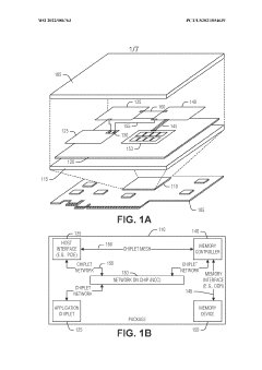
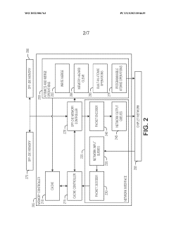
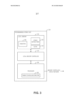
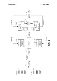
Non-homogeneous chiplets
PatentActiveUS12013810B2
Innovation
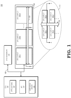
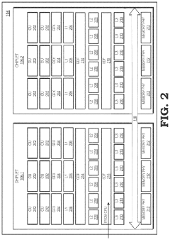
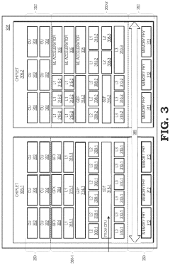
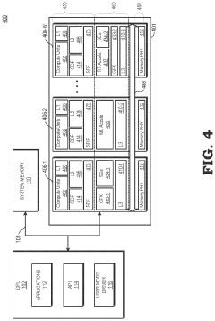
- The implementation of a semiconductor module with multiple interconnected GPU chiplets, each with a common set of circuitry modules and non-homogeneous supporting modules, allows for efficient distribution of workloads across chiplets, utilizing an interconnect that provides coherent memory access and routes commands to appropriate chiplets based on their specific capabilities.
Chiplet Design Standards and Protocols
Chiplet design standards and protocols play a crucial role in the development and implementation of chiplet-based architectures. These standards ensure interoperability, consistency, and efficiency across different chiplet designs and manufacturers. The primary focus of these standards is to establish common interfaces, communication protocols, and packaging techniques that enable seamless integration of multiple chiplets into a single system.
One of the most prominent standards in chiplet design is the Advanced Interface Bus (AIB), developed by Intel. AIB provides a high-bandwidth, low-power interface for chip-to-chip communication, allowing for efficient data transfer between chiplets. This standard has gained significant traction in the industry due to its flexibility and scalability, making it suitable for a wide range of applications.
Another important standard is the Universal Chiplet Interconnect Express (UCIe), which aims to create an open ecosystem for chiplet-based designs. UCIe defines a standardized die-to-die interconnect that enables chiplets from different vendors to work together seamlessly. This standard addresses the need for a unified approach to chiplet integration, promoting innovation and competition in the semiconductor industry.
The Open Compute Project (OCP) has also contributed to chiplet design standards through its Open Domain-Specific Architecture (ODSA) workgroup. The ODSA focuses on developing open standards for chiplet-based systems, including specifications for physical interfaces, protocols, and software abstractions. These efforts aim to reduce design complexity and time-to-market for chiplet-based products.
In terms of protocols, the Bunch of Wires (BoW) interface has emerged as a popular choice for chiplet-to-chiplet communication. BoW offers a simple, low-cost solution for connecting chiplets, making it particularly attractive for applications that require moderate bandwidth and power efficiency. The protocol's simplicity also contributes to easier implementation and verification processes.
For high-performance computing applications, the High Bandwidth Memory (HBM) interface standard has become increasingly important in chiplet designs. HBM allows for the integration of high-bandwidth memory chiplets with processing chiplets, enabling significant improvements in memory bandwidth and power efficiency.
As chiplet designs continue to evolve, new standards and protocols are being developed to address emerging challenges. These include efforts to standardize thermal management techniques, power delivery systems, and testing methodologies for chiplet-based architectures. The ongoing collaboration between industry leaders, research institutions, and standards organizations is crucial in driving the adoption and advancement of chiplet technology.
Energy Efficiency in Chiplet Designs
Energy efficiency has become a critical consideration in chiplet designs, driven by the increasing demand for high-performance computing systems with reduced power consumption. Chiplet architectures offer significant advantages in this regard, allowing for more efficient power distribution and management across multiple smaller dies compared to monolithic designs.
One of the key strategies for improving energy efficiency in chiplet designs is the implementation of fine-grained power gating. This technique enables individual chiplets or specific functional blocks within chiplets to be powered down when not in use, significantly reducing static power consumption. Advanced power management controllers integrated into the chiplet design can dynamically adjust voltage and frequency levels based on workload requirements, further optimizing energy usage.
Thermal management plays a crucial role in enhancing energy efficiency for chiplet-based systems. The modular nature of chiplets allows for more effective heat dissipation through improved thermal interface materials and advanced packaging technologies. This enables higher sustained performance levels without excessive power consumption due to thermal throttling.
Interconnect technologies between chiplets have also seen significant advancements in energy efficiency. The adoption of high-bandwidth, low-power interfaces such as Advanced Interface Bus (AIB) and Universal Chiplet Interconnect Express (UCIe) has reduced the power overhead associated with inter-chiplet communication. These interfaces utilize advanced signaling techniques and power-aware protocols to minimize energy consumption during data transfer.
Memory integration strategies in chiplet designs have evolved to prioritize energy efficiency. The use of High Bandwidth Memory (HBM) stacks directly integrated with compute chiplets reduces the power required for data movement between processing elements and memory. Additionally, the implementation of on-chip caches and intelligent data prefetching mechanisms helps minimize off-chip memory accesses, further reducing overall system power consumption.
Software-hardware co-design approaches have emerged as a powerful tool for optimizing energy efficiency in chiplet-based systems. By developing software that is aware of the underlying chiplet architecture, developers can create more energy-efficient algorithms that leverage the unique characteristics of chiplet designs. This includes optimizing task scheduling and data movement to minimize inter-chiplet communication and maximize the utilization of power-efficient chiplets.
As chiplet designs continue to evolve, emerging technologies such as photonic interconnects and advanced packaging materials promise to further enhance energy efficiency. These innovations will enable even higher bandwidth communication between chiplets while significantly reducing power consumption, paving the way for more sustainable and high-performance computing systems in the future.
Unlock deeper insights with PatSnap Eureka Quick Research — get a full tech report to explore trends and direct your research. Try now!
Generate Your Research Report Instantly with AI Agent
Supercharge your innovation with PatSnap Eureka AI Agent Platform!