

How Chiplet Architecture Drives Infrastructure Modernization?
JUL 16, 20259 MIN READ
Generate Your Research Report Instantly with AI Agent
Patsnap Eureka helps you evaluate technical feasibility & market potential.
Chiplet Evolution and Objectives
Chiplet architecture represents a paradigm shift in semiconductor design, evolving from traditional monolithic chip designs to a more modular and flexible approach. This evolution began in the early 2010s as a response to the increasing challenges of scaling traditional integrated circuits. The primary objective of chiplet technology is to overcome the limitations of Moore's Law by enabling the integration of multiple smaller dies (chiplets) into a single package, thereby improving performance, reducing costs, and enhancing manufacturing yields.
The development of chiplet architecture has been driven by several key factors. First, the increasing complexity and size of modern chips have made it increasingly difficult and expensive to manufacture large monolithic dies with acceptable yields. Chiplets address this by allowing manufacturers to produce smaller, more manageable dies that can be combined to create high-performance systems. This approach also enables the mixing of different process nodes within a single package, optimizing cost and performance for different components.
Another crucial objective of chiplet technology is to improve time-to-market for new products. By leveraging a modular approach, companies can reuse existing chiplet designs across multiple products, significantly reducing development time and costs. This modularity also allows for greater customization, as different combinations of chiplets can be used to create a wide range of products tailored to specific market needs.
The evolution of chiplet architecture has been marked by several significant milestones. In 2017, AMD introduced its Infinity Fabric interconnect technology, which enabled the company to create multi-chip module (MCM) designs for its Ryzen and EPYC processors. This approach allowed AMD to compete effectively with Intel in the high-performance computing market. Intel, in turn, introduced its own chiplet-based designs with the Foveros 3D packaging technology in 2018, demonstrating the industry-wide shift towards modular chip designs.
As chiplet technology continues to evolve, its objectives have expanded to address emerging challenges in infrastructure modernization. One key goal is to improve energy efficiency in data centers and edge computing environments. By optimizing the design and integration of chiplets, manufacturers can create more power-efficient systems that reduce overall energy consumption and operational costs for large-scale infrastructure deployments.
Furthermore, chiplet architecture aims to enhance scalability and flexibility in hardware design, allowing for more rapid adaptation to changing computational demands. This is particularly crucial in the context of infrastructure modernization, where the ability to quickly deploy and upgrade hardware resources is essential for maintaining competitive advantage in fast-evolving markets such as cloud computing, artificial intelligence, and 5G networks.
Market Demand Analysis
The market demand for chiplet architecture is experiencing significant growth, driven by the increasing need for high-performance computing in various sectors. As traditional monolithic chip designs reach their physical limits, chiplets offer a scalable and cost-effective solution to meet the evolving requirements of modern infrastructure.
In the data center and cloud computing market, the demand for chiplet-based solutions is particularly strong. These environments require powerful processors capable of handling massive workloads, and chiplets provide the flexibility to create custom configurations tailored to specific use cases. The ability to mix and match different chiplets allows for optimized performance, power efficiency, and cost-effectiveness, which are crucial factors for data center operators and cloud service providers.
The telecommunications industry is another key driver of chiplet demand, especially with the ongoing rollout of 5G networks and the anticipated transition to 6G. Chiplet architecture enables the development of more efficient and compact base stations, as well as edge computing devices that can process data closer to the source. This aligns with the industry's push towards network function virtualization and software-defined networking.
In the artificial intelligence and machine learning sector, chiplets are gaining traction due to their ability to integrate specialized accelerators alongside general-purpose processors. This heterogeneous computing approach is essential for handling the complex and diverse workloads associated with AI training and inference tasks. The modular nature of chiplets allows for easier updates and upgrades, which is crucial in the rapidly evolving field of AI.
The automotive industry is also showing increased interest in chiplet technology, particularly for advanced driver assistance systems (ADAS) and autonomous vehicles. These applications require high-performance, low-latency computing capabilities that can be efficiently delivered through chiplet-based designs. The ability to integrate different types of processors and accelerators on a single package is particularly valuable for meeting the diverse processing needs of modern vehicles.
Consumer electronics, including smartphones, tablets, and laptops, represent another growing market for chiplet architecture. As devices become more powerful and feature-rich, chiplets offer a way to pack more computing power into smaller form factors while managing power consumption and heat dissipation.
The industrial sector is adopting chiplet technology for applications in automation, robotics, and the Internet of Things (IoT). The modular nature of chiplets allows for the creation of specialized processors that can be optimized for specific industrial tasks, such as real-time control systems or edge computing in smart factories.
Overall, the market demand for chiplet architecture is driven by the need for more powerful, efficient, and flexible computing solutions across a wide range of industries. As infrastructure modernization continues to accelerate, chiplets are poised to play a crucial role in enabling the next generation of high-performance computing systems.
Chiplet Tech Challenges
Chiplet architecture, while promising significant advancements in semiconductor design and performance, faces several critical challenges that need to be addressed for widespread adoption and successful implementation in infrastructure modernization.
One of the primary challenges is the complexity of integration. Chiplets require sophisticated packaging technologies to connect multiple dies efficiently. The design and manufacturing of advanced interposers and substrates capable of supporting high-bandwidth, low-latency connections between chiplets is a significant hurdle. This integration complexity extends to thermal management, as the dense packaging of multiple chiplets can lead to increased heat generation and potential hotspots.
Standardization poses another major challenge. The lack of universal standards for chiplet interfaces and protocols hinders interoperability between chiplets from different manufacturers. This absence of standardization can limit design flexibility and increase development costs, potentially slowing down the adoption of chiplet-based solutions in infrastructure modernization efforts.
Testing and validation of chiplet-based systems present unique difficulties. Traditional testing methods may not be sufficient for complex multi-die packages, requiring new approaches to ensure reliability and performance. This challenge is particularly critical in infrastructure applications where system stability and longevity are paramount.
Power management and distribution across multiple chiplets is another area of concern. Efficiently delivering power to various components within a chiplet-based system, while maintaining optimal performance and minimizing power loss, requires innovative power delivery network designs and management strategies.
The challenge of yield management also comes into play. While chiplets can potentially improve overall yield by allowing the use of smaller, more manageable die sizes, the complexity of assembling multiple chiplets introduces new yield considerations in the packaging and integration stages.
Data security and integrity in chiplet-based systems present additional challenges. As data moves between chiplets, ensuring secure and error-free transmission becomes crucial, especially in sensitive infrastructure applications.
Lastly, the economic challenges cannot be overlooked. The initial investment required for transitioning to chiplet-based designs, including new design tools, manufacturing processes, and supply chain adjustments, can be substantial. Balancing these costs against the potential long-term benefits is a critical consideration for companies looking to leverage chiplet architecture in infrastructure modernization.
Current Chiplet Solutions
01 Chiplet-based System-on-Chip (SoC) Design
Modernizing SoC architecture by utilizing chiplets, which are smaller, modular components that can be combined to create more complex systems. This approach allows for greater flexibility, scalability, and cost-effectiveness in chip design, enabling the integration of diverse functionalities and technologies on a single package.- Chiplet-based system architecture: Modern chiplet architecture involves designing systems using multiple smaller chips (chiplets) interconnected on a single package. This approach allows for more flexible and scalable designs, improved performance, and potentially lower manufacturing costs. The infrastructure for chiplet-based systems includes advanced packaging technologies, high-speed interconnects, and standardized interfaces for seamless integration.
- Interconnect technologies for chiplets: Advanced interconnect technologies are crucial for chiplet architecture modernization. These include high-bandwidth, low-latency connections between chiplets, such as silicon interposers, advanced packaging techniques, and optical interconnects. The focus is on improving data transfer rates, reducing power consumption, and enhancing overall system performance in multi-chiplet designs.
- Power management and thermal solutions: Efficient power management and thermal solutions are essential for chiplet-based systems. This includes advanced cooling techniques, dynamic power gating, and intelligent power distribution across multiple chiplets. The goal is to optimize energy efficiency and manage heat dissipation in densely packed chiplet architectures, ensuring reliable operation and extended lifespan of the components.
- Standardization and interoperability: Standardization efforts are crucial for chiplet architecture infrastructure modernization. This includes developing common interfaces, protocols, and design standards to ensure interoperability between chiplets from different manufacturers. Standardization facilitates a more diverse and competitive ecosystem, enabling mix-and-match capabilities in chiplet-based system designs.
- Software and firmware optimization: Software and firmware optimization is essential for fully leveraging chiplet-based architectures. This includes developing specialized operating systems, drivers, and middleware that can efficiently manage and utilize multi-chiplet systems. Advanced scheduling algorithms, load balancing techniques, and memory management strategies are implemented to maximize performance and energy efficiency in chiplet-based infrastructures.
02 Interconnect Technologies for Chiplet Integration
Development of advanced interconnect technologies to facilitate high-speed, low-latency communication between chiplets. This includes innovations in die-to-die interfaces, through-silicon vias (TSVs), and packaging techniques to enable efficient data transfer and power distribution across chiplet-based systems.Expand Specific Solutions03 Heterogeneous Integration and Packaging
Advancements in packaging technologies to support the integration of diverse chiplets, potentially manufactured using different process nodes or technologies. This includes 2.5D and 3D packaging solutions, as well as novel thermal management approaches to address the challenges of high-density chiplet integration.Expand Specific Solutions04 Power Management and Optimization for Chiplet Architectures
Innovative power management techniques tailored for chiplet-based systems, including dynamic power gating, voltage scaling, and thermal management strategies. These approaches aim to optimize energy efficiency and performance across heterogeneous chiplet configurations.Expand Specific Solutions05 Design and Verification Tools for Chiplet-based Systems
Development of specialized EDA tools and methodologies to support the design, simulation, and verification of chiplet-based architectures. This includes software for chiplet floorplanning, system-level optimization, and automated testing of multi-chiplet configurations.Expand Specific Solutions
Key Industry Players
The chiplet architecture market is in a growth phase, driven by increasing demand for high-performance computing and AI applications. Major players like Intel, AMD, and TSMC are investing heavily in this technology, with the market expected to reach significant size in the coming years. The technology's maturity is advancing rapidly, with companies like Micron, Samsung, and Xilinx making notable progress. Intel's disaggregated design approach and AMD's chiplet-based Ryzen processors demonstrate the technology's practical applications. However, challenges remain in standardization and integration, indicating that the technology is still evolving. As more companies like Huawei and GLOBALFOUNDRIES enter the space, competition is intensifying, potentially accelerating innovation and market adoption of chiplet architecture in infrastructure modernization efforts.
Intel Corp.
Technical Solution: Intel's chiplet architecture, exemplified by their Foveros 3D packaging technology, enables the stacking of multiple chiplets vertically[1]. This approach allows for the integration of diverse IP blocks and process nodes within a single package. Intel's Ponte Vecchio GPU, built on this architecture, incorporates over 40 tiles across five process nodes[2]. The company's advanced packaging technologies, including EMIB (Embedded Multi-die Interconnect Bridge) and Foveros, facilitate high-bandwidth connections between chiplets, enabling modular designs that can be customized for specific applications[3]. This modularity supports infrastructure modernization by allowing for more flexible and scalable hardware configurations, potentially reducing costs and improving performance in data centers and edge computing environments.
Strengths: Highly flexible and customizable designs, improved performance density, and potential for cost reduction. Weaknesses: Increased complexity in manufacturing and thermal management, potential for higher initial costs.
Xilinx, Inc.
Technical Solution: Xilinx, now part of AMD, has implemented chiplet architecture in their Adaptive Compute Acceleration Platform (ACAP) products, such as the Versal series[9]. This architecture combines FPGA fabric, ARM CPU cores, and dedicated AI engines on a single chip, using a modular approach. The chiplet design allows Xilinx to integrate different types of processing elements optimized for specific tasks, providing a flexible and scalable platform for a wide range of applications. In the context of infrastructure modernization, Xilinx's chiplet-based ACAPs offer programmable acceleration for data center, edge computing, and 5G infrastructure, enabling more efficient and adaptable hardware solutions for evolving computational needs[10].
Strengths: High flexibility and programmability, efficient integration of diverse processing elements. Weaknesses: Complexity in programming and optimizing for specific applications, potentially higher costs compared to fixed-function ASICs.
Core Chiplet Innovations
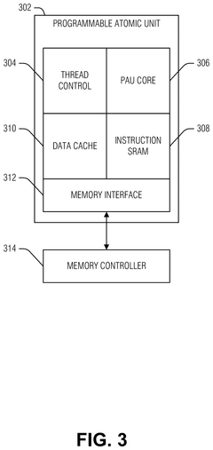
Parking threads in barrel processor for managing hazard clearing
PatentPendingUS20240419534A1
Innovation
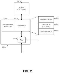
- The implementation of a compute-near-memory (CNM) system with hybrid threading processors and fabrics that allow on-demand thread rescheduling and efficient data access, utilizing chiplet-based architectures for scalable and high-bandwidth memory access, and custom compute fabrics to enhance performance and reduce latency.
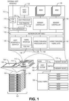
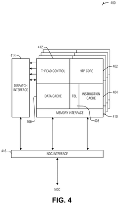
Thread scheduling control and memory splitting in a barrel processor
PatentWO2022086763A1
Innovation
- Implementing a thread scheduling control mechanism that organizes threads into separate groups, each with its own memory device, and alternates between groups for read and write access to reduce memory contention, allowing threads to progress through the pipeline more efficiently and reducing power draw.
Infrastructure Impact
Chiplet architecture is revolutionizing the way modern infrastructure is designed and implemented, driving significant advancements in performance, scalability, and efficiency. This innovative approach to semiconductor design has far-reaching implications for various sectors of infrastructure, including data centers, telecommunications networks, and high-performance computing systems.
One of the primary impacts of chiplet architecture on infrastructure modernization is the enhanced ability to scale computing power. By allowing the integration of multiple smaller dies onto a single package, chiplets enable the creation of more powerful and complex processors without the limitations of traditional monolithic designs. This scalability is particularly crucial for data centers and cloud computing infrastructure, where the demand for processing power continues to grow exponentially.
The modular nature of chiplet architecture also contributes to improved energy efficiency in infrastructure systems. By optimizing the design and manufacturing process for individual chiplets, engineers can create more power-efficient components that, when combined, result in overall lower power consumption for high-performance computing systems. This reduction in energy usage not only leads to cost savings but also aligns with the growing emphasis on sustainable and environmentally friendly infrastructure solutions.
Chiplet architecture is driving advancements in network infrastructure as well. The ability to integrate specialized chiplets for networking functions, such as packet processing and encryption, allows for the development of more capable and flexible network equipment. This enhanced functionality supports the ongoing evolution of 5G and future 6G networks, enabling faster data transmission, lower latency, and improved network capacity.
In the realm of edge computing, chiplet architecture is facilitating the creation of more powerful and versatile edge devices. By incorporating various specialized chiplets into a single package, edge computing nodes can be designed to handle a wider range of tasks, from AI inference to real-time data processing. This flexibility is crucial for supporting the growing Internet of Things (IoT) ecosystem and enabling more sophisticated applications at the network edge.
The impact of chiplet architecture extends to the field of artificial intelligence and machine learning infrastructure. The ability to combine high-performance computing chiplets with specialized AI accelerators in a single package allows for the development of more efficient and powerful AI systems. This integration is particularly beneficial for data centers and research institutions that require substantial computational resources for training and deploying large-scale AI models.
Standardization Efforts
Standardization efforts play a crucial role in the widespread adoption and implementation of chiplet architecture for infrastructure modernization. As the industry recognizes the potential of chiplet-based designs, several organizations and consortia have emerged to establish common standards and protocols.
One of the most prominent initiatives is the Universal Chiplet Interconnect Express (UCIe) consortium, which aims to create an open industry standard for die-to-die interconnects. UCIe focuses on defining a common physical layer, protocol stack, and software model to enable seamless integration of chiplets from different vendors. This standardization effort is backed by major industry players, including Intel, AMD, Arm, and TSMC, highlighting its significance in shaping the future of chiplet-based systems.
Another important standardization effort is the Open Compute Project (OCP), which has established the Open Domain-Specific Architecture (ODSA) workgroup. The ODSA workgroup is dedicated to developing open standards for chiplet-based designs, with a focus on creating a marketplace for chiplets and enabling interoperability between different vendors' components.
The JEDEC Solid State Technology Association has also been actively involved in chiplet standardization efforts. They have formed the JC70 Committee on Wide I/O Memories, which is working on developing standards for high-bandwidth memory interfaces that are critical for chiplet-based designs.
In addition to these industry-wide efforts, individual companies are also contributing to standardization through their own initiatives. For example, AMD's Infinity Fabric and Intel's Advanced Interface Bus (AIB) are proprietary interconnect technologies that have been made available to the wider industry, promoting standardization and interoperability.
These standardization efforts are essential for overcoming the challenges associated with chiplet integration, such as ensuring compatibility between chiplets from different manufacturers, optimizing performance, and reducing design complexity. By establishing common protocols and interfaces, these initiatives are paving the way for a more diverse and innovative ecosystem of chiplet-based solutions.
As standardization efforts continue to mature, they are expected to accelerate the adoption of chiplet architecture in various infrastructure modernization projects. This will enable more efficient and flexible system designs, ultimately driving innovation and performance improvements across a wide range of applications, from data centers and edge computing to telecommunications and high-performance computing systems.
Unlock deeper insights with Patsnap Eureka Quick Research — get a full tech report to explore trends and direct your research. Try now!
Generate Your Research Report Instantly with AI Agent
Supercharge your innovation with Patsnap Eureka AI Agent Platform!