Chiplet Innovations: A Stepping Stone to Future Developments
JUL 16, 20259 MIN READ
Generate Your Research Report Instantly with AI Agent
PatSnap Eureka helps you evaluate technical feasibility & market potential.
Chiplet Evolution
The evolution of chiplets represents a significant paradigm shift in semiconductor design and manufacturing. This innovative approach emerged as a response to the increasing challenges faced by traditional monolithic chip designs, particularly in terms of scalability, performance, and cost-effectiveness.
In the early stages of chiplet development, the focus was primarily on disaggregating large, complex System-on-Chip (SoC) designs into smaller, more manageable components. This initial phase saw the introduction of basic chiplet architectures, where different functional blocks were separated onto individual dies and then interconnected using advanced packaging technologies.
As the concept gained traction, the industry witnessed a rapid progression in chiplet design methodologies and integration techniques. The development of high-bandwidth, low-latency die-to-die interconnects became a critical enabler for chiplet technology. This led to the creation of various interconnect standards and protocols, such as AMD's Infinity Fabric and Intel's Advanced Interface Bus (AIB), which facilitated seamless communication between chiplets.
The next phase of chiplet evolution focused on enhancing modularity and reusability. This approach allowed semiconductor companies to mix and match different chiplets, each potentially manufactured using different process nodes, to create customized solutions for specific applications. This modularity not only improved design flexibility but also significantly reduced development costs and time-to-market for new products.
Recent advancements in chiplet technology have seen a push towards greater standardization and interoperability. Industry consortiums, such as the Universal Chiplet Interconnect Express (UCIe), have been formed to establish common standards for chiplet interfaces and packaging. This move towards standardization aims to create an ecosystem where chiplets from different vendors can be easily integrated, fostering innovation and competition in the semiconductor industry.
Looking ahead, the future of chiplet evolution is poised to embrace even more advanced integration techniques. Three-dimensional (3D) chiplet stacking is emerging as a promising direction, offering the potential for higher performance, lower power consumption, and further miniaturization. Additionally, the integration of heterogeneous technologies, such as combining digital logic with analog, RF, and photonic components in a single package, is opening up new possibilities for highly specialized and efficient system designs.
As chiplet technology continues to mature, we can expect to see its application expand beyond high-performance computing and data centers into areas such as edge computing, artificial intelligence accelerators, and next-generation mobile devices. This ongoing evolution of chiplet technology is not just a stepping stone but a fundamental shift in how we approach semiconductor design and manufacturing, paving the way for more innovative and efficient computing solutions in the future.
Market Demand Analysis
The market demand for chiplet technology has been steadily growing, driven by the increasing complexity and performance requirements of modern computing systems. As traditional monolithic chip designs approach their physical limits, chiplets offer a promising solution to continue advancing semiconductor capabilities while managing costs and improving yields.
In the data center and high-performance computing sectors, there is a strong demand for chiplet-based solutions that can deliver higher compute density, improved energy efficiency, and reduced latency. Cloud service providers and enterprises are seeking ways to handle the exponential growth in data processing and artificial intelligence workloads, making chiplets an attractive option for scaling performance beyond what traditional monolithic designs can offer.
The telecommunications industry, particularly with the rollout of 5G and future 6G networks, is another key driver of chiplet demand. These advanced networks require high-performance, low-power chips that can be customized for specific applications, making chiplets an ideal fit for next-generation base stations and network infrastructure.
Consumer electronics, including smartphones, tablets, and laptops, are also contributing to the growing market for chiplets. As devices become more powerful and feature-rich, manufacturers are looking to chiplet technology to integrate diverse functionalities while maintaining compact form factors and managing power consumption.
The automotive sector is emerging as a significant market for chiplets, driven by the increasing electrification of vehicles and the development of advanced driver assistance systems (ADAS) and autonomous driving technologies. These applications require high-performance, reliable, and power-efficient semiconductor solutions that can be tailored to specific vehicle platforms.
Market analysts project substantial growth in the chiplet market over the coming years. The flexibility and scalability offered by chiplets are expected to enable new product categories and accelerate innovation across various industries. This growth is further supported by the increasing adoption of heterogeneous computing architectures, which leverage different types of processors and accelerators to optimize performance for specific workloads.
However, the market demand for chiplets is not without challenges. Standardization efforts are crucial to ensure interoperability between chiplets from different manufacturers, which is essential for widespread adoption. Additionally, the ecosystem for chiplet design, manufacturing, and integration is still evolving, requiring significant investments in tools, processes, and infrastructure.
Technical Challenges
Chiplet technology, while promising significant advancements in semiconductor design and manufacturing, faces several critical challenges that need to be addressed for widespread adoption and continued innovation. One of the primary hurdles is the complexity of integration. Connecting multiple chiplets seamlessly requires sophisticated packaging technologies and precise alignment, which can be technically demanding and costly.
Thermal management presents another significant challenge. As chiplets are packed closely together, heat dissipation becomes a critical issue. Ensuring efficient cooling across the entire package, especially in high-performance applications, requires innovative thermal solutions and careful design considerations.
Power distribution and signal integrity pose additional technical difficulties. The interconnects between chiplets must be able to handle high-speed data transmission while minimizing power loss and signal degradation. This necessitates advanced materials and design techniques to maintain performance across the entire multi-chip package.
Standardization remains a key challenge in the chiplet ecosystem. The lack of universal standards for chiplet interfaces and protocols can hinder interoperability between chiplets from different manufacturers. This fragmentation could potentially slow down industry-wide adoption and limit the full potential of mix-and-match chip design.
Testing and quality assurance present unique challenges in chiplet-based systems. Ensuring the reliability and performance of individual chiplets, as well as the integrated package, requires new testing methodologies and equipment. This is particularly crucial as defects in a single chiplet could impact the entire system's functionality.
Yield management is another area of concern. While chiplets can potentially improve overall yield by allowing manufacturers to use smaller, higher-yield die, the complexity of integrating multiple chiplets can introduce new yield challenges at the packaging level.
Cost considerations remain a significant hurdle, especially for widespread adoption. While chiplet technology promises long-term cost benefits through improved yield and flexibility, the initial investment in new design tools, manufacturing processes, and testing equipment can be substantial.
Lastly, the industry faces challenges in design and simulation tools. Existing EDA (Electronic Design Automation) tools may need significant updates to effectively handle the complexities of multi-chiplet designs, including thermal, power, and signal integrity considerations across the entire package.
Current Chiplet Solutions
01 Chiplet integration and packaging
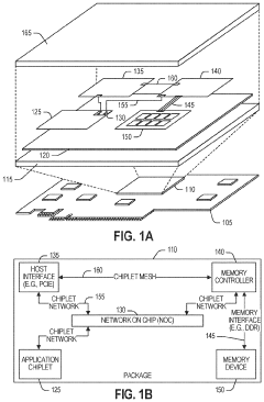
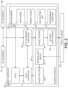
Chiplets are integrated circuit dies that can be combined to form larger, more complex systems. This approach allows for modular design and improved manufacturing yields. Advanced packaging techniques are used to interconnect these chiplets, enabling high-performance and cost-effective multi-chip solutions.- Chiplet integration and packaging technologies: Advanced packaging technologies for integrating multiple chiplets into a single package. This includes methods for interconnecting chiplets, thermal management, and optimizing performance in multi-chip modules. These technologies enable the creation of more complex and powerful systems while overcoming limitations of monolithic chip designs.
- Chiplet-based system-on-chip (SoC) architectures: Design methodologies for creating modular SoC architectures using chiplets. This approach allows for mixing and matching different functional blocks, improving scalability, and reducing development costs. It enables the creation of customized solutions for various applications while reusing validated chiplet designs.
- Interconnect technologies for chiplets: Development of high-speed, low-latency interconnect technologies specifically designed for chiplet-to-chiplet communication. This includes advanced interface protocols, die-to-die bridges, and novel packaging substrates that enable efficient data transfer between chiplets in a multi-chip module.
- Power management and thermal solutions for chiplet designs: Innovative approaches to managing power consumption and heat dissipation in chiplet-based systems. This includes techniques for dynamic power gating, thermal-aware chiplet placement, and advanced cooling solutions tailored for multi-chip modules to ensure optimal performance and reliability.
- Chiplet design and verification methodologies: Specialized design and verification techniques for chiplet-based systems. This includes methods for ensuring compatibility between chiplets from different vendors, standardizing chiplet interfaces, and developing efficient testing strategies for multi-chip modules. These methodologies aim to streamline the development process and improve the reliability of chiplet-based products.
02 Interconnect technologies for chiplets
Various interconnect technologies are employed to facilitate communication between chiplets. These may include advanced interposers, silicon bridges, or through-silicon vias (TSVs). The choice of interconnect technology impacts the overall performance, power efficiency, and form factor of the chiplet-based system.Expand Specific Solutions03 Thermal management in chiplet designs
Effective thermal management is crucial in chiplet-based systems due to the high power density and potential hotspots. Innovative cooling solutions, such as integrated liquid cooling or advanced heat spreaders, are developed to maintain optimal operating temperatures and ensure reliability.Expand Specific Solutions04 Power distribution and management for chiplets
Efficient power distribution and management are essential for chiplet-based designs. This includes developing advanced power delivery networks, implementing fine-grained power gating, and utilizing adaptive voltage scaling techniques to optimize energy consumption across the chiplet system.Expand Specific Solutions05 Testing and validation of chiplet-based systems
Comprehensive testing and validation methodologies are crucial for ensuring the reliability and performance of chiplet-based systems. This includes developing specialized test structures, implementing built-in self-test capabilities, and creating advanced simulation and modeling techniques to verify the functionality and performance of the integrated chiplet system.Expand Specific Solutions
Key Industry Players
The chiplet innovation landscape is characterized by intense competition and rapid technological advancements. The market is in a growth phase, with major players like Intel, Micron Technology, and QUALCOMM investing heavily in research and development. The global chiplet market size is expanding, driven by increasing demand for high-performance computing and AI applications. Technologically, chiplets are maturing, with companies like TSMC and AMD making significant strides. However, challenges remain in standardization and integration. Emerging players such as Xidian University and MetaX Integrated Circuits are also contributing to the field, indicating a diverse and dynamic competitive environment.
Intel Corp.
Technical Solution: Intel's Foveros 3D packaging technology is a key innovation in chiplet design. It allows for the vertical stacking of diverse silicon dies, enabling the integration of different process nodes and IP blocks in a single package[1]. Intel has demonstrated this technology in products like Lakefield processors, which combine high-performance cores with energy-efficient cores. The company is also developing Foveros Omni and Foveros Direct for even more advanced chiplet integration[2]. Intel's EMIB (Embedded Multi-die Interconnect Bridge) technology complements Foveros by providing high-bandwidth connections between chiplets in a 2.5D arrangement[3].
Strengths: Advanced 3D packaging capabilities, proven track record in high-volume manufacturing. Weaknesses: Potential thermal management challenges in densely stacked designs, higher production costs compared to traditional monolithic chips.
Semiconductor Manufacturing International (Shanghai) Corp.
Technical Solution: SMIC has been investing in advanced packaging technologies to support chiplet-based designs. The company has developed capabilities in 2.5D and 3D integration, including through-silicon via (TSV) technology and chip-on-wafer-on-substrate (CoWoS) packaging[6]. SMIC's approach to chiplet innovation focuses on providing cost-effective solutions for a wide range of applications, from consumer electronics to automotive and industrial sectors. The company has been working on improving its interposer technology and fine-pitch micro-bump connections to enable higher-density chiplet integration[7].
Strengths: Cost-effective manufacturing capabilities, growing expertise in advanced packaging. Weaknesses: Limited access to cutting-edge process nodes due to trade restrictions, potential challenges in competing with more advanced chiplet technologies from global leaders.
Core Chiplet Patents
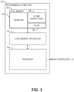
Self-scheduling threads in a programmable atomic unit
PatentPendingUS20240086200A1
Innovation
- Implementing self-scheduling threads by using thread identifiers and a thread ready-to-run queue, where only threads without resource contention are executed, and thread IDs are removed and re-enqueued based on memory request completion, eliminating the need for traditional hazard tracking mechanisms.


Method of executing programmable atomic unit resources within a multi-process system
PatentActiveUS12020062B2
Innovation
- A method is disclosed that involves determining a unique identifier for a programmable atomic transaction within a process, using a mapping table to generate a system-wide identifier, and issuing requests to a memory controller to perform the transaction, allowing for efficient execution and response handling through a programmable atomic unit.
Chiplet Ecosystem
The Chiplet ecosystem represents a complex network of interconnected players, technologies, and processes that collectively drive the advancement and adoption of chiplet-based designs. At its core, this ecosystem comprises semiconductor manufacturers, packaging companies, electronic design automation (EDA) tool providers, and intellectual property (IP) vendors, all working in tandem to enable the creation of high-performance, cost-effective chiplet solutions.
Central to the chiplet ecosystem are the foundries and integrated device manufacturers (IDMs) that produce the individual chiplets. These entities invest heavily in advanced manufacturing processes and packaging technologies to create diverse chiplet offerings. Complementing their efforts are the packaging companies that specialize in advanced integration techniques such as 2.5D and 3D packaging, which are crucial for interconnecting multiple chiplets into a cohesive system.
EDA tool providers play a pivotal role in the ecosystem by developing sophisticated software solutions that enable the design, verification, and testing of chiplet-based systems. These tools are essential for managing the complexity of chiplet integration, optimizing performance, and ensuring compatibility across different chiplets.
IP vendors contribute significantly to the ecosystem by offering pre-designed and pre-verified chiplet components, ranging from processor cores to specialized accelerators. This modular approach allows system designers to rapidly compose complex systems using a mix of custom and off-the-shelf chiplets, accelerating time-to-market and reducing development costs.
The chiplet ecosystem also encompasses standards organizations and industry consortia that work towards establishing common interfaces and protocols. These efforts are crucial for ensuring interoperability between chiplets from different vendors and promoting a more open and competitive marketplace.
Research institutions and universities contribute to the ecosystem by pushing the boundaries of chiplet technology through fundamental research and innovation. Their work often leads to breakthroughs in areas such as interconnect technologies, thermal management, and novel integration approaches.
As the chiplet ecosystem continues to evolve, it is increasingly attracting attention from system integrators and original equipment manufacturers (OEMs) who see the potential for creating highly customized, high-performance computing solutions. This growing interest is driving further investment and innovation across the ecosystem, reinforcing its importance in shaping the future of semiconductor design and manufacturing.
Standardization Efforts
Standardization efforts in the chiplet industry are crucial for fostering innovation and ensuring interoperability among different manufacturers' components. The development of common interfaces and protocols is essential for the widespread adoption of chiplet technology. Several industry consortia and organizations are actively working towards establishing standards for chiplet integration.
One of the most prominent initiatives is the Universal Chiplet Interconnect Express (UCIe) consortium, which aims to create an open industry standard for die-to-die interconnects. UCIe focuses on defining physical and protocol layer specifications for chiplet-to-chiplet communication. This standard is gaining traction among major semiconductor companies, including Intel, AMD, Arm, and TSMC, who recognize the need for a unified approach to chiplet integration.
Another significant standardization effort is the Open Compute Project's (OCP) Chiplet Design Exchange (CDX) working group. CDX is developing standards for chiplet-based system design, focusing on creating a common language and methodology for describing chiplet characteristics and interfaces. This initiative aims to streamline the design process and enable more efficient collaboration between chiplet providers and system integrators.
The JEDEC Solid State Technology Association is also contributing to chiplet standardization through its JC-63 Committee on Chiplets. This committee is working on developing standards for chiplet-based memory systems, addressing the unique challenges of integrating memory components in a chiplet architecture.
In addition to these industry-wide efforts, individual companies are also pushing for standardization through their own initiatives. For example, Intel's Advanced Interface Bus (AIB) and AMD's Infinity Fabric are proprietary interconnect technologies that have been made available for licensing, potentially serving as de facto standards in certain market segments.
The importance of these standardization efforts cannot be overstated. They are essential for reducing design complexity, lowering costs, and accelerating time-to-market for chiplet-based products. Standardized interfaces and protocols enable a more diverse ecosystem of chiplet suppliers and system integrators, fostering innovation and competition in the semiconductor industry.
However, challenges remain in achieving widespread adoption of chiplet standards. Different companies may have conflicting interests, and there is a risk of fragmentation if multiple competing standards emerge. Overcoming these challenges will require continued collaboration and compromise among industry players to ensure that the benefits of chiplet technology can be fully realized across the semiconductor ecosystem.
Unlock deeper insights with PatSnap Eureka Quick Research — get a full tech report to explore trends and direct your research. Try now!
Generate Your Research Report Instantly with AI Agent
Supercharge your innovation with PatSnap Eureka AI Agent Platform!