

How Chiplets Enable Efficient Application Platform Adaptation?
JUL 16, 20259 MIN READ
Generate Your Research Report Instantly with AI Agent
PatSnap Eureka helps you evaluate technical feasibility & market potential.
Chiplet Technology Evolution and Objectives
Chiplet technology has emerged as a revolutionary approach in the semiconductor industry, offering a paradigm shift in chip design and manufacturing. The evolution of chiplets can be traced back to the early 2010s when the limitations of traditional monolithic chip designs became increasingly apparent. As Moore's Law began to slow down, chiplets presented a viable solution to continue scaling performance and efficiency.
The primary objective of chiplet technology is to enable more efficient and flexible chip designs by breaking down complex systems into smaller, modular components. This approach allows for the integration of different process nodes, intellectual property (IP) blocks, and functionalities onto a single package, effectively overcoming the limitations of monolithic designs. By leveraging chiplets, manufacturers can optimize performance, power consumption, and cost-effectiveness across various applications.
The evolution of chiplet technology has been driven by several key factors. First, the increasing demand for specialized computing solutions in areas such as artificial intelligence, data centers, and edge computing has necessitated more adaptable chip architectures. Chiplets provide the flexibility to mix and match different components to meet specific application requirements. Second, the rising costs and technical challenges associated with advanced process nodes have made it economically viable to combine mature and cutting-edge technologies within a single package.
Throughout its development, chiplet technology has seen significant milestones. The introduction of 2.5D and 3D packaging technologies has been crucial in enabling efficient chiplet integration. Advanced interconnect technologies, such as silicon interposers and through-silicon vias (TSVs), have played a vital role in facilitating high-bandwidth, low-latency communication between chiplets. Furthermore, the development of industry standards, like the Universal Chiplet Interconnect Express (UCIe), has been instrumental in promoting interoperability and accelerating chiplet adoption across the industry.
Looking ahead, the objectives of chiplet technology are multifaceted. One primary goal is to further enhance performance and energy efficiency by enabling more granular optimization of chip components. This includes the ability to combine chiplets from different vendors and process nodes seamlessly. Another objective is to reduce time-to-market and development costs by promoting reusability and modularity in chip design. Additionally, chiplet technology aims to improve yield rates by allowing manufacturers to produce smaller, less complex dies with higher success rates.
As the semiconductor industry continues to evolve, chiplet technology is poised to play a crucial role in enabling efficient application platform adaptation. By providing a flexible and scalable approach to chip design, chiplets offer a pathway to meet the diverse and ever-changing demands of modern computing applications. The ongoing development of chiplet technology promises to unlock new possibilities in performance, efficiency, and customization across a wide range of electronic devices and systems.
Market Demand for Adaptable Application Platforms
The market demand for adaptable application platforms has been steadily growing in recent years, driven by the increasing complexity and diversity of computing needs across various industries. As businesses and organizations face rapidly evolving technological landscapes, there is a pressing need for flexible and scalable solutions that can efficiently adapt to changing requirements without necessitating complete system overhauls.
One of the key factors fueling this demand is the exponential growth of data-intensive applications, such as artificial intelligence, machine learning, and big data analytics. These applications require substantial computing power and specialized hardware configurations, which can vary significantly depending on the specific use case. Traditional monolithic chip designs often struggle to meet these diverse and dynamic needs, leading to inefficiencies and increased costs.
The rise of edge computing and Internet of Things (IoT) devices has further amplified the need for adaptable platforms. These distributed systems demand tailored solutions that can balance performance, power efficiency, and connectivity across a wide range of deployment scenarios. As a result, businesses are seeking platforms that can be easily customized and optimized for specific edge computing tasks without compromising overall system performance.
In the telecommunications sector, the rollout of 5G networks and the anticipated transition to 6G have created a surge in demand for flexible hardware solutions. Network operators require platforms that can be rapidly reconfigured to support evolving network standards and protocols, ensuring seamless upgrades and minimizing infrastructure costs.
The automotive industry is another significant driver of demand for adaptable platforms. As vehicles become increasingly connected and autonomous, there is a growing need for flexible computing architectures that can accommodate a wide range of sensors, processing units, and communication systems. These platforms must be capable of supporting over-the-air updates and integrating new features throughout the vehicle's lifecycle.
Cloud service providers and data centers are also major contributors to the market demand for adaptable platforms. With the continuous evolution of cloud computing technologies and the need to support diverse workloads, these organizations require hardware solutions that can be easily scaled and reconfigured to meet changing customer requirements and optimize resource utilization.
The financial sector, particularly in areas such as high-frequency trading and blockchain technologies, has shown a strong interest in adaptable platforms. These applications demand ultra-low latency and high throughput, coupled with the ability to quickly adapt to new algorithms and market conditions.
As sustainability becomes an increasingly important consideration, there is a growing demand for platforms that can optimize power consumption and improve energy efficiency across various computing scenarios. Adaptable solutions that can dynamically adjust their performance and power profiles based on workload requirements are highly sought after in this context.
Current Challenges in Chiplet Integration
While chiplets offer significant advantages in terms of scalability, performance, and cost-effectiveness, their integration presents several challenges that need to be addressed for widespread adoption. One of the primary hurdles is the development of standardized interfaces for chiplet-to-chiplet communication. The lack of universally accepted standards hampers interoperability between chiplets from different manufacturers, limiting design flexibility and increasing integration complexity.
Another critical challenge lies in the thermal management of chiplet-based systems. As multiple chiplets are integrated into a single package, heat dissipation becomes more complex, potentially leading to hotspots and performance degradation. Innovative cooling solutions and thermal-aware design strategies are necessary to maintain optimal performance and reliability.
Power distribution and management across chiplets pose additional difficulties. Ensuring efficient power delivery to each chiplet while minimizing power loss and maintaining signal integrity requires sophisticated power distribution networks and advanced packaging technologies. This challenge is particularly pronounced in high-performance computing applications where power consumption is a critical factor.
The testing and validation of chiplet-based systems present unique challenges compared to traditional monolithic designs. Identifying and isolating faults within a multi-chiplet system can be more complex, requiring advanced testing methodologies and equipment. Additionally, ensuring the reliability and longevity of the interconnects between chiplets is crucial for overall system performance and durability.
Manufacturing and assembly processes for chiplet integration also face significant hurdles. Achieving high yields and maintaining consistent quality across multiple chiplets from potentially different foundries requires precise alignment and bonding techniques. The development of cost-effective and scalable manufacturing processes for chiplet integration is essential for widespread adoption.
Lastly, the design and verification of chiplet-based systems present new challenges to engineers. Traditional EDA tools and methodologies may not be fully equipped to handle the complexities of multi-chiplet designs, necessitating the development of new tools and design flows. This includes addressing issues such as timing closure across chiplet boundaries, managing signal integrity in high-speed interfaces, and optimizing system-level performance.
Overcoming these challenges requires collaborative efforts from semiconductor manufacturers, packaging companies, EDA tool providers, and standards organizations. As the industry continues to invest in chiplet technology, addressing these integration challenges will be crucial for realizing the full potential of chiplet-based designs in enabling efficient application platform adaptation.
Existing Chiplet-based Platform Solutions
01 Chiplet interconnect optimization
Improving the efficiency of chiplets by optimizing the interconnect architecture between different chiplet components. This includes developing advanced packaging technologies and high-bandwidth interfaces to reduce communication latency and power consumption between chiplets.- Chiplet interconnect optimization: Improving the efficiency of chiplets by optimizing the interconnect architecture between different chiplet components. This includes developing advanced packaging technologies and high-bandwidth interfaces to reduce communication latency and power consumption between chiplets.
- Thermal management for chiplet designs: Enhancing chiplet efficiency through improved thermal management techniques. This involves developing innovative cooling solutions and thermal dissipation methods specifically tailored for multi-chiplet architectures to maintain optimal performance and reliability.
- Power distribution optimization in chiplet systems: Improving the efficiency of chiplets by optimizing power distribution across the multi-chip module. This includes developing advanced power delivery networks and voltage regulation techniques to ensure efficient power usage and minimize power loss in chiplet-based designs.
- Chiplet-specific design and manufacturing processes: Developing specialized design methodologies and manufacturing processes tailored for chiplet-based architectures. This includes creating new EDA tools, design rules, and fabrication techniques to optimize the efficiency and yield of chiplet production and integration.
- Heterogeneous integration of chiplets: Enhancing system efficiency through the integration of diverse chiplets with different functionalities or process nodes. This approach allows for optimizing each chiplet for its specific task while maintaining overall system performance and power efficiency.
02 Thermal management for chiplets
Enhancing chiplet efficiency through improved thermal management techniques. This involves developing innovative cooling solutions and thermal interface materials to dissipate heat more effectively, allowing chiplets to operate at higher frequencies and with better overall performance.Expand Specific Solutions03 Power distribution optimization
Optimizing power distribution across chiplets to improve overall system efficiency. This includes developing advanced power delivery networks, voltage regulation techniques, and power gating strategies to minimize power consumption and maximize performance of chiplet-based designs.Expand Specific Solutions04 Chiplet integration and packaging
Improving chiplet efficiency through advanced integration and packaging technologies. This involves developing novel 2.5D and 3D packaging solutions, as well as heterogeneous integration techniques to optimize the overall system performance and reduce form factor.Expand Specific Solutions05 Chiplet-specific design and optimization tools
Developing specialized design and optimization tools for chiplet-based architectures. This includes creating software for chiplet floorplanning, interconnect optimization, and system-level performance analysis to improve the overall efficiency of chiplet designs.Expand Specific Solutions
Key Players in Chiplet Ecosystem
The chiplet technology market is in a growth phase, with increasing adoption across various sectors. The market size is expanding rapidly, driven by demand for more efficient and scalable semiconductor solutions. Technological maturity varies among players, with established companies like Intel, AMD, and TSMC leading in chiplet development and implementation. Emerging players such as Primemas are introducing innovative approaches to chiplet design. Companies like Micron, SK hynix, and Xilinx are leveraging their expertise in memory and programmable logic to advance chiplet integration. The competitive landscape is dynamic, with both traditional semiconductor giants and specialized startups vying for market share in this evolving field.
Xilinx, Inc.
Technical Solution: Xilinx, now part of AMD, has developed the Adaptive Compute Acceleration Platform (ACAP) that leverages chiplet technology. Their Versal ACAP architecture combines programmable logic, DSP engines, and AI cores on a single platform[4]. This approach allows for customizable configurations tailored to specific application needs. Xilinx's chiplet strategy focuses on heterogeneous integration, enabling the combination of different process nodes and IP blocks to optimize performance and power efficiency[5]. The company has also invested in advanced packaging technologies to support high-bandwidth die-to-die interconnects essential for chiplet-based designs[6].
Strengths: High degree of customization, adaptability to various workloads, and integration of diverse computing elements. Weaknesses: Complexity in programming and optimization, potentially higher initial costs compared to monolithic designs.
Intel Corp.
Technical Solution: Intel's chiplet technology, known as "Foveros," enables 3D stacking of chiplets, allowing for efficient application platform adaptation. This approach combines high-performance compute tiles with low-power base tiles, optimizing power and performance for diverse applications[1]. Intel's Meteor Lake processors utilize this technology, integrating CPU, GPU, and AI accelerator tiles on a single package[2]. The company has also introduced advanced packaging technologies like EMIB (Embedded Multi-die Interconnect Bridge) to facilitate high-bandwidth, low-latency connections between chiplets[3].
Strengths: Flexibility in combining different IP blocks, improved power efficiency, and scalability. Weaknesses: Increased complexity in design and manufacturing, potential thermal management challenges in 3D stacked configurations.
Core Innovations in Chiplet Interconnect Technologies
Method for configuring multiple input-output channels
PatentWO2022046284A1
Innovation
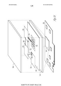
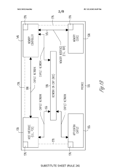
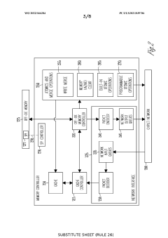
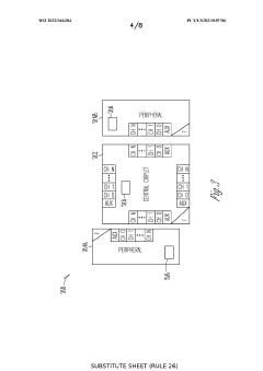
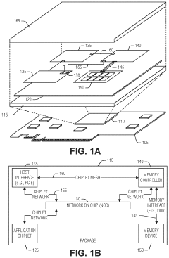
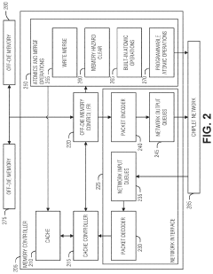
- The implementation of a Chiplet Protocol Interface (CPI) network with Advanced Interface Bus (AIB) channels and credit-based flow control, allowing for flexible virtual channel mapping and minimizing latency and energy consumption through packetized protocols and serialization-deserialization (SERDES) hardware, while enabling efficient inter-chiplet communication.
Variable pipeline length in a barrel-multithreaded processor
PatentActiveUS11847464B2
Innovation
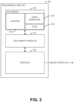
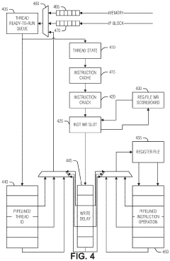
- Implementing a variable pipeline length in processors to allow instructions to complete and writeback early, and using a scoreboard to detect and manage register writeback conflicts, ensuring efficient thread rescheduling and minimizing idle cycles.
Standardization Efforts in Chiplet Design
Standardization efforts in chiplet design are crucial for enabling efficient application platform adaptation through chiplets. These efforts aim to establish common interfaces, protocols, and design methodologies that facilitate interoperability and integration of chiplets from different vendors.
One of the most significant standardization initiatives is the Universal Chiplet Interconnect Express (UCIe) consortium. UCIe is developing an open industry standard for die-to-die interconnects, which is essential for creating modular chip designs. This standard defines physical and protocol layers for chiplet-to-chiplet communication, ensuring compatibility across different manufacturers and technologies.
Another important standardization effort is the Open Compute Project's (OCP) Chiplet Design Exchange (CDX) format. CDX aims to create a common language for describing chiplet designs, making it easier for different companies to collaborate and integrate their chiplets into larger systems. This standardization helps reduce design complexity and time-to-market for chiplet-based products.
The CHIPS Alliance, an open-source hardware initiative, is also contributing to chiplet standardization. They are working on developing open-source tools and methodologies for chiplet design and integration, which can help lower the barriers to entry for smaller companies and accelerate innovation in the field.
In addition to these industry-led efforts, government agencies are also supporting chiplet standardization. For example, the U.S. Department of Defense's CHIPS program (Common Heterogeneous Integration and IP Reuse Strategies) is funding research and development of standards for modular chip designs, with a focus on defense and aerospace applications.
Standardization efforts also extend to packaging technologies, which are critical for chiplet integration. The Joint Electron Device Engineering Council (JEDEC) is working on standards for advanced packaging technologies, including those used in chiplet-based designs. These standards help ensure consistency and reliability in chiplet integration across different manufacturers.
As chiplet technology continues to evolve, ongoing standardization efforts will play a crucial role in enabling efficient application platform adaptation. By establishing common interfaces and design methodologies, these standards will facilitate the creation of more flexible, scalable, and cost-effective chip designs that can be easily customized for specific applications and markets.
Economic Impact of Chiplet-based Platforms
The adoption of chiplet-based platforms is poised to have a significant economic impact across the semiconductor industry and related sectors. This innovative approach to chip design and manufacturing offers substantial cost savings and improved scalability, which are likely to reshape the economics of semiconductor production and application development.
One of the primary economic benefits of chiplet-based platforms is the potential for reduced manufacturing costs. By allowing manufacturers to produce smaller, more specialized chips and integrate them into a single package, chiplets enable more efficient use of silicon wafers and potentially higher yields. This approach can lead to lower production costs per unit, especially for high-performance computing applications that traditionally require large, monolithic chips.
The modular nature of chiplets also introduces greater flexibility in product development and customization. Companies can mix and match different chiplets to create a wide range of products tailored to specific market segments or customer needs. This adaptability can lead to faster time-to-market for new products and potentially lower development costs, as companies can reuse existing chiplet designs across multiple product lines.
Furthermore, chiplet-based platforms may democratize access to advanced semiconductor technologies. Smaller companies and startups, which may not have the resources to develop entire system-on-chip (SoC) solutions, can leverage chiplets to create competitive products by focusing on their core competencies and integrating with other specialized chiplets. This could foster innovation and increase competition in the semiconductor market.
The economic impact extends beyond the semiconductor industry itself. As chiplet-based platforms enable more efficient and powerful computing solutions, they can drive advancements in various application areas such as artificial intelligence, edge computing, and 5G networks. These technological improvements can, in turn, stimulate economic growth in sectors that rely on advanced computing capabilities.
However, the transition to chiplet-based platforms also presents economic challenges. The industry will need to invest in new design tools, manufacturing processes, and testing methodologies specific to chiplet integration. Additionally, the development of standards for chiplet interfaces and packaging will be crucial for realizing the full economic potential of this approach.
In conclusion, the economic impact of chiplet-based platforms is likely to be far-reaching, offering opportunities for cost reduction, increased innovation, and market expansion. As the technology matures and adoption grows, it has the potential to reshape the competitive landscape of the semiconductor industry and drive economic growth in related sectors.
Unlock deeper insights with PatSnap Eureka Quick Research — get a full tech report to explore trends and direct your research. Try now!
Generate Your Research Report Instantly with AI Agent
Supercharge your innovation with PatSnap Eureka AI Agent Platform!