Chiplet Configurations: Balancing Performance and Cost
JUL 16, 20259 MIN READ
Generate Your Research Report Instantly with AI Agent
Patsnap Eureka helps you evaluate technical feasibility & market potential.
Chiplet Tech Evolution
The evolution of chiplet technology represents a significant paradigm shift in semiconductor design and manufacturing. This approach, which involves breaking down complex chip designs into smaller, more manageable components, has gained traction as a solution to the challenges posed by traditional monolithic chip designs.
The chiplet concept emerged in response to the increasing difficulties in scaling traditional monolithic chips. As Moore's Law began to slow down, chiplets offered a way to continue improving performance and functionality while managing costs and manufacturing complexity. The evolution of chiplet technology can be traced through several key stages.
In the early 2010s, the initial concept of chiplets began to take shape. Companies like AMD started exploring the potential of multi-chip modules (MCMs) as a way to overcome the limitations of single-die designs. This marked the beginning of a new era in chip design, focusing on modular architectures.
The mid-2010s saw the first commercial implementations of chiplet-based designs. AMD's Zen architecture, introduced in 2017, utilized a chiplet approach for their Ryzen processors. This demonstrated the viability of chiplets in high-performance computing applications and set the stage for wider adoption.
As the technology matured, the industry began to recognize the need for standardization. The development of interface standards like Universal Chiplet Interconnect Express (UCIe) in the late 2010s and early 2020s was crucial in enabling interoperability between chiplets from different manufacturers.
The early 2020s marked a period of rapid advancement and widespread adoption of chiplet technology. Major players like Intel, TSMC, and Samsung invested heavily in chiplet-based designs, recognizing their potential to address the scaling challenges of traditional monolithic chips.
Recent developments have focused on enhancing chiplet integration and performance. Advanced packaging technologies like 2.5D and 3D integration have enabled more complex and efficient chiplet configurations. These advancements have allowed for higher bandwidth, lower latency, and improved power efficiency in chiplet-based systems.
Looking forward, the chiplet evolution is expected to continue with a focus on heterogeneous integration. This involves combining chiplets with different functionalities and process nodes, allowing for more specialized and efficient designs. The development of AI-assisted design tools for chiplet-based systems is also emerging as a key trend, potentially revolutionizing the chip design process.
Market Demand Analysis
The market demand for chiplet configurations has been steadily growing, driven by the increasing need for high-performance computing solutions across various industries. As traditional monolithic chip designs reach their physical and economic limits, chiplet-based architectures have emerged as a promising alternative to balance performance and cost.
The semiconductor industry has witnessed a significant shift towards chiplet technology, with major players like AMD, Intel, and TSMC investing heavily in this approach. This trend is primarily fueled by the demand for more powerful and efficient processors in data centers, cloud computing, artificial intelligence, and edge computing applications.
In the data center market, chiplet configurations are particularly attractive due to their ability to deliver higher performance and improved power efficiency. The modular nature of chiplets allows for more flexible and scalable designs, enabling data center operators to optimize their infrastructure based on specific workload requirements. This flexibility has led to increased adoption of chiplet-based solutions in enterprise and hyperscale data centers.
The artificial intelligence and machine learning sectors have also shown strong demand for chiplet configurations. These technologies require massive computational power, which can be efficiently delivered through chiplet-based designs. The ability to combine different types of specialized processing units, such as CPUs, GPUs, and AI accelerators, on a single package has made chiplets an ideal solution for AI workloads.
In the consumer electronics market, chiplet configurations are gaining traction in high-end devices such as gaming consoles and premium smartphones. The improved performance and power efficiency offered by chiplet designs allow manufacturers to create more powerful and feature-rich devices while managing thermal constraints and battery life.
The automotive industry is another sector driving demand for chiplet configurations. As vehicles become increasingly connected and autonomous, the need for advanced computing power in automotive systems has grown significantly. Chiplet-based solutions offer the performance and flexibility required for next-generation automotive applications, including advanced driver assistance systems (ADAS) and infotainment systems.
The market demand for chiplet configurations is also influenced by the ongoing global chip shortage and supply chain disruptions. The modular nature of chiplets allows for more efficient use of manufacturing resources and potentially faster time-to-market for new products. This has made chiplet-based designs an attractive option for companies looking to mitigate supply chain risks and improve product availability.
As the technology matures and manufacturing processes improve, the demand for chiplet configurations is expected to expand into new markets and applications. The ability to mix and match different types of chiplets from various manufacturers opens up possibilities for more customized and cost-effective solutions across a wide range of industries.
Chiplet Challenges
The adoption of chiplet technology presents several significant challenges that must be addressed to fully realize its potential in balancing performance and cost. One of the primary obstacles is the complexity of inter-chiplet communication. As multiple chiplets are integrated onto a single package, ensuring efficient and high-bandwidth communication between these components becomes crucial. This requires advanced packaging technologies and sophisticated interconnect solutions, which can increase manufacturing complexity and costs.
Another major challenge lies in thermal management. With multiple chiplets in close proximity, heat dissipation becomes a critical concern. Effective cooling solutions must be developed to maintain optimal operating temperatures across all chiplets, which can be particularly challenging given the varying power requirements and heat generation of different components.
Design and integration complexities also pose significant hurdles. Chiplet-based systems require careful consideration of power distribution, signal integrity, and clock synchronization across multiple dies. This necessitates advanced design tools and methodologies capable of handling the intricacies of multi-chiplet architectures.
Testing and validation of chiplet-based systems present another set of challenges. Traditional testing methods may not be sufficient for assessing the performance and reliability of interconnected chiplets. New testing strategies and equipment may need to be developed to ensure the quality and reliability of these complex systems.
The lack of standardization in chiplet interfaces and protocols is a significant barrier to widespread adoption. Without industry-wide standards, interoperability between chiplets from different manufacturers becomes difficult, limiting the flexibility and cost-effectiveness of chiplet-based designs.
Manufacturing yield is another critical concern. While chiplets can potentially improve overall yield by allowing the use of smaller, more easily manufactured dies, the integration process itself introduces new yield challenges. Defects in the packaging or interconnect process can render an entire multi-chiplet system unusable, potentially offsetting the yield advantages at the die level.
Lastly, the economic challenges of chiplet adoption cannot be overlooked. While chiplets offer the potential for cost savings in the long term, the initial investment in research, development, and new manufacturing processes can be substantial. Companies must carefully weigh these upfront costs against the potential benefits and market demands.
Current Configurations
01 Chiplet interconnect optimization
Optimizing chiplet interconnects is crucial for improving performance and reducing costs in multi-chip configurations. This involves developing advanced packaging technologies, high-bandwidth interfaces, and efficient communication protocols between chiplets. By enhancing interconnect efficiency, designers can minimize latency, increase data transfer rates, and reduce power consumption, leading to improved overall system performance and cost-effectiveness.- Chiplet interconnect optimization: Optimizing chiplet interconnects is crucial for improving performance and reducing costs in multi-chip configurations. This involves developing advanced packaging technologies, high-bandwidth interfaces, and efficient communication protocols between chiplets. By enhancing interconnect efficiency, designers can minimize latency, increase data transfer rates, and reduce power consumption, leading to improved overall system performance and cost-effectiveness.
- Heterogeneous chiplet integration: Integrating heterogeneous chiplets allows for the combination of different process technologies and specialized functions within a single package. This approach enables designers to optimize performance and cost by selecting the most suitable process node for each chiplet based on its specific requirements. By leveraging the strengths of various chiplet types, manufacturers can achieve better overall system performance while potentially reducing production costs.
- Power management and thermal optimization: Effective power management and thermal optimization are essential for maximizing chiplet performance while minimizing costs. This involves implementing advanced power gating techniques, dynamic voltage and frequency scaling, and efficient heat dissipation methods. By optimizing power consumption and thermal characteristics, designers can improve energy efficiency, extend battery life in mobile devices, and reduce cooling costs in data center applications.
- Chiplet yield improvement and cost reduction: Improving chiplet yield and reducing manufacturing costs are critical factors in chiplet-based designs. This involves developing advanced defect detection and isolation techniques, implementing redundancy and repair mechanisms, and optimizing the chiplet manufacturing process. By enhancing yield and reducing production costs, manufacturers can improve the overall cost-effectiveness of chiplet-based systems and accelerate their adoption in various applications.
- Chiplet-based system-level optimization: Optimizing chiplet-based systems at the system level is crucial for achieving the best balance between performance and cost. This involves developing advanced design methodologies, system-level simulation tools, and optimization algorithms to evaluate and improve the overall system architecture. By considering factors such as chiplet placement, interconnect topology, and workload distribution, designers can create more efficient and cost-effective chiplet-based solutions for various applications.
02 Heterogeneous chiplet integration
Integrating heterogeneous chiplets allows for the combination of different process nodes and specialized functionalities within a single package. This approach enables designers to optimize performance and cost by using the most suitable technology for each component. By leveraging the strengths of various chiplet types, such as high-performance cores, memory, and I/O interfaces, system architects can achieve a balance between performance requirements and manufacturing costs.Expand Specific Solutions03 Power management and thermal optimization
Effective power management and thermal optimization are essential for maximizing chiplet performance while minimizing costs. This involves implementing advanced power gating techniques, dynamic voltage and frequency scaling, and efficient heat dissipation methods. By optimizing power consumption and thermal characteristics, designers can improve energy efficiency, extend battery life in mobile devices, and reduce cooling costs in data center applications.Expand Specific Solutions04 Chiplet yield improvement and cost reduction
Improving chiplet yield and reducing manufacturing costs are critical factors in chiplet-based designs. This includes developing advanced defect detection and isolation techniques, implementing redundancy and repair mechanisms, and optimizing chiplet sizes for maximum yield. By enhancing yield rates and minimizing waste, manufacturers can significantly reduce production costs and improve the overall economic viability of chiplet-based solutions.Expand Specific Solutions05 Chiplet-based system-level optimization
Optimizing chiplet-based systems at the architectural level is crucial for balancing performance and cost. This involves developing efficient chiplet floorplanning techniques, implementing intelligent resource allocation algorithms, and designing scalable architectures that can adapt to varying performance requirements. By optimizing the overall system architecture, designers can achieve better performance-to-cost ratios and create more flexible and adaptable computing solutions.Expand Specific Solutions
Key Chiplet Players
The chiplet configuration market is in a growth phase, driven by increasing demand for high-performance computing solutions. Major players like Intel, AMD, and TSMC are actively developing and implementing chiplet technologies to address performance and cost challenges. The market size is expanding rapidly, with projections indicating significant growth in the coming years. Technologically, chiplet configurations are maturing, with companies like Micron, Infineon, and GlobalFoundries making strides in interconnect technologies and integration methods. However, challenges remain in standardization and yield optimization. Emerging players such as Primemas and Intelligo Technology are also contributing to innovation in this space, potentially disrupting the market with novel approaches to chiplet design and integration.
Intel Corp.
Technical Solution: Intel's approach to Chiplet configurations focuses on their Foveros 3D packaging technology and EMIB (Embedded Multi-die Interconnect Bridge). Foveros allows for vertical stacking of chiplets, while EMIB provides high-bandwidth connections between chiplets in a 2D arrangement. Intel's Ponte Vecchio GPU, built on these technologies, demonstrates their advanced chiplet strategy, combining over 40 tiles manufactured on different process nodes[1]. This approach allows Intel to mix and match different IP blocks and process technologies, optimizing performance and cost. Intel's chiplets are connected using high-bandwidth die-to-die interfaces, enabling data rates up to 5.4 Gb/s/pin[2], which is crucial for maintaining performance in multi-chiplet designs.
Strengths: Flexibility in combining different process nodes and IP blocks, high-bandwidth die-to-die connections, and vertical integration capabilities. Weaknesses: Complexity in design and manufacturing, potential yield issues with multiple chiplets, and higher initial costs for implementation.
Advanced Micro Devices, Inc.
Technical Solution: AMD's chiplet strategy revolves around their Infinity Fabric interconnect technology, which allows for efficient communication between multiple chiplets. Their approach is exemplified in the Ryzen and EPYC processor lines, where they use smaller, more cost-effective chiplets manufactured on advanced process nodes for CPU cores, combined with I/O dies on mature processes. This configuration enables AMD to achieve high core counts while maintaining good yields and cost-effectiveness. AMD's 3rd Gen EPYC processors, for instance, can incorporate up to eight CPU chiplets with 7nm cores connected to a central I/O die[3]. The company has also introduced 3D V-Cache technology, stacking additional cache memory directly on top of CPU chiplets, further enhancing performance without increasing the overall package footprint[4].
Strengths: Scalability, cost-effectiveness for high-core-count processors, and ability to optimize different functions on appropriate process nodes. Weaknesses: Potential latency issues between chiplets, complexity in thermal management, and reliance on advanced packaging technologies.
Core Chiplet Patents
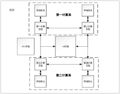
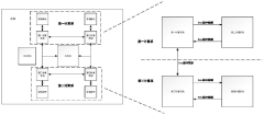
A chip and control method based on chiplet architecture
PatentActiveCN115617739B
Innovation
- Using the Chiplet architecture, the chip is decomposed into multiple small chips (CPU core, IO core, computing core, storage unit, silicon adapter board and substrate), and data is exchanged through the UCIe bus to achieve synchronization and synchronization of computing cores. detection, supports performance, security, single-line and low-power consumption modes, and uses CoWoS packaging technology to reduce costs.
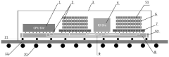
Homogeneous chiplets configurable as a two-dimensional system or a three-dimensional system
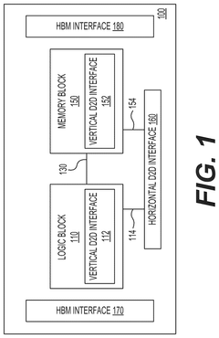
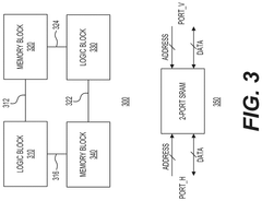
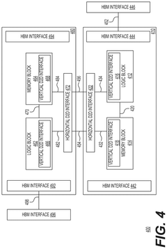
PatentPendingUS20250038120A1
Innovation
- A homogeneous chiplet system is introduced, comprising vertically stacked or horizontally coupled chiplets with on-die interconnect structures and vertical die-to-die interconnection structures, allowing for efficient data signal transfer and reducing latency.
Chiplet Ecosystem
The chiplet ecosystem has emerged as a critical component in the semiconductor industry, revolutionizing the way integrated circuits are designed and manufactured. This ecosystem encompasses a wide range of technologies, standards, and players that collectively enable the development and production of chiplet-based systems. At its core, the chiplet approach involves disaggregating complex System-on-Chip (SoC) designs into smaller, more manageable functional blocks that can be manufactured separately and then integrated using advanced packaging technologies.
One of the key elements of the chiplet ecosystem is the development of standardized interfaces and protocols that allow for seamless integration of chiplets from different vendors. Organizations such as the Open Compute Project (OCP) and JEDEC have been instrumental in driving the creation of these standards, with initiatives like Universal Chiplet Interconnect Express (UCIe) gaining significant traction in the industry. These standards not only facilitate interoperability but also promote a more open and collaborative ecosystem.
The chiplet ecosystem also includes a diverse range of packaging technologies that enable the integration of multiple chiplets into a single package. Advanced packaging solutions such as 2.5D and 3D integration, silicon interposers, and fan-out wafer-level packaging (FOWLP) play a crucial role in realizing the full potential of chiplet-based designs. These technologies allow for high-bandwidth, low-latency connections between chiplets, as well as improved thermal management and power efficiency.
Another important aspect of the chiplet ecosystem is the development of design tools and methodologies that support the creation of chiplet-based systems. Electronic Design Automation (EDA) companies have been adapting their software suites to address the unique challenges posed by chiplet designs, including multi-die floor planning, system-level simulation, and die-to-die interface optimization. These tools are essential for enabling designers to effectively leverage the chiplet approach and maximize its benefits.
The chiplet ecosystem also encompasses a growing network of foundries, Outsourced Semiconductor Assembly and Test (OSAT) providers, and Intellectual Property (IP) vendors. This network supports the diverse manufacturing and integration requirements of chiplet-based designs, offering a range of process nodes, packaging options, and pre-validated IP blocks. The collaboration between these various players is crucial for driving innovation and reducing time-to-market for chiplet-based products.
Cost-Perf Tradeoffs
The balance between cost and performance is a critical consideration in chiplet configurations. As chiplet technology continues to evolve, manufacturers face the challenge of optimizing designs to achieve the best possible performance while maintaining cost-effectiveness. This delicate equilibrium requires careful analysis of various factors and trade-offs.
One of the primary advantages of chiplet designs is the ability to mix and match different process nodes within a single package. This flexibility allows for the use of advanced nodes for performance-critical components while utilizing more mature, cost-effective nodes for less demanding functions. However, the decision-making process involves weighing the benefits of improved performance against the increased costs associated with cutting-edge fabrication processes.
Interconnect technology plays a crucial role in chiplet performance and cost trade-offs. High-bandwidth, low-latency interconnects are essential for maximizing the potential of chiplet designs, but they also contribute significantly to overall costs. Manufacturers must evaluate different interconnect solutions, such as silicon interposers, organic substrates, or advanced packaging technologies, to find the optimal balance between performance gains and cost implications.
The number and size of chiplets within a configuration also impact the cost-performance equation. Smaller chiplets may offer better yield and cost advantages but could introduce additional complexity in terms of packaging and interconnects. Conversely, larger chiplets may simplify integration but potentially increase manufacturing costs due to lower yields on advanced process nodes.
Power consumption is another critical factor in the cost-performance trade-off. While higher performance often correlates with increased power requirements, it also leads to greater thermal management challenges and potentially higher operating costs. Designers must consider innovative cooling solutions and power-efficient architectures to strike the right balance between performance and energy consumption.
The choice of packaging technology significantly influences both cost and performance. Advanced packaging techniques, such as 2.5D and 3D integration, can offer substantial performance improvements but come with higher manufacturing costs. Manufacturers must carefully assess whether the performance gains justify the additional expenses associated with these advanced packaging methods.
Ultimately, the optimal chiplet configuration depends on the specific application requirements and target market. High-performance computing and data center applications may justify higher costs for maximum performance, while consumer electronics might prioritize cost-effectiveness. Manufacturers must conduct thorough cost-benefit analyses to determine the most suitable chiplet configuration for each use case, considering factors such as time-to-market, scalability, and long-term cost implications.
Unlock deeper insights with Patsnap Eureka Quick Research — get a full tech report to explore trends and direct your research. Try now!
Generate Your Research Report Instantly with AI Agent
Supercharge your innovation with Patsnap Eureka AI Agent Platform!