Chiplet Ecosystem Expansion: Opportunities and Challenges
JUL 16, 20259 MIN READ
Generate Your Research Report Instantly with AI Agent
PatSnap Eureka helps you evaluate technical feasibility & market potential.
Chiplet Evolution
The evolution of chiplets represents a paradigm shift in semiconductor design and manufacturing, driven by the need to overcome the limitations of traditional monolithic chip architectures. This transition began in the early 2010s as semiconductor companies sought ways to improve performance, reduce costs, and enhance scalability in chip production.
Initially, chiplets were primarily used in high-performance computing applications, where the demand for increased processing power and memory bandwidth was most acute. Companies like AMD pioneered the use of chiplets in their EPYC server processors, demonstrating significant improvements in performance and efficiency compared to monolithic designs.
As the technology matured, the adoption of chiplets expanded to other sectors, including consumer electronics, telecommunications, and automotive industries. This broader application was facilitated by advancements in packaging technologies, such as 2.5D and 3D integration, which allowed for more efficient interconnects between chiplets.
The evolution of chiplets has been marked by several key milestones. The development of standardized interfaces, such as AMD's Infinity Fabric and Intel's Advanced Interface Bus (AIB), has been crucial in enabling interoperability between chiplets from different manufacturers. This standardization has paved the way for a more open and collaborative ecosystem.
Another significant development has been the improvement in die-to-die communication technologies. The introduction of high-bandwidth, low-latency interconnects has reduced the performance penalties associated with multi-chip designs, making chiplets increasingly competitive with monolithic architectures across a wider range of applications.
The chiplet ecosystem has also seen advancements in thermal management and power distribution techniques, addressing some of the early challenges associated with multi-chip packages. These improvements have expanded the feasibility of chiplet-based designs in power-sensitive applications, such as mobile devices and edge computing systems.
Recent years have witnessed a growing focus on heterogeneous integration, combining chiplets with different process nodes or even different materials on a single package. This approach allows for optimized performance and cost-effectiveness by utilizing the most appropriate manufacturing process for each component of the system.
As the chiplet ecosystem continues to evolve, we are seeing increased collaboration between semiconductor companies, foundries, and packaging specialists. This collaborative approach is essential for addressing the complex challenges of chiplet design, manufacturing, and integration, and is driving further innovation in the field.
Market Demand Analysis
The Chiplet ecosystem is experiencing rapid growth, driven by increasing demand for high-performance computing solutions across various industries. Market analysis indicates a significant shift towards modular chip designs, with chiplets playing a crucial role in addressing the limitations of traditional monolithic architectures.
The global semiconductor market, valued at $555.9 billion in 2021, is projected to reach $1,380.8 billion by 2029, with chiplet technology contributing substantially to this growth. The demand for chiplet-based solutions is particularly strong in data centers, artificial intelligence, and edge computing applications, where performance, power efficiency, and scalability are paramount.
In the data center segment, the need for more powerful and efficient processors is driving the adoption of chiplet-based designs. Major cloud service providers and enterprise customers are seeking solutions that can handle increasingly complex workloads while minimizing power consumption and reducing total cost of ownership. This trend is expected to continue as data processing requirements grow exponentially.
The artificial intelligence and machine learning sectors are also fueling demand for chiplet-based solutions. As AI models become more sophisticated and computationally intensive, there is a growing need for specialized processors that can efficiently handle these workloads. Chiplets offer the flexibility to combine different types of processing units, such as CPUs, GPUs, and AI accelerators, on a single package, enabling optimized performance for AI applications.
Edge computing represents another significant market opportunity for chiplet technology. As more devices become connected and require local processing capabilities, there is a rising demand for compact, power-efficient computing solutions. Chiplets enable the creation of customized, high-performance edge devices that can meet the specific requirements of various IoT applications.
The automotive industry is emerging as a key driver of chiplet adoption, particularly in the development of advanced driver assistance systems (ADAS) and autonomous vehicles. These applications require high-performance, low-power computing solutions that can operate reliably in challenging environments. Chiplet-based designs offer the potential to meet these demanding requirements while providing the necessary flexibility for future upgrades.
Consumer electronics, including smartphones, tablets, and wearables, represent another growing market for chiplet technology. As consumers demand more powerful and feature-rich devices, manufacturers are exploring chiplet-based solutions to deliver enhanced performance and functionality within compact form factors.
The market demand for chiplet-based solutions is further bolstered by the increasing focus on sustainability and energy efficiency. By enabling more efficient use of silicon and reducing overall power consumption, chiplets align with the growing emphasis on environmentally friendly technologies across industries.
Technical Challenges
The expansion of the Chiplet ecosystem presents several significant technical challenges that need to be addressed for successful implementation and widespread adoption. One of the primary hurdles is the development of advanced packaging technologies capable of integrating diverse chiplets with high performance and reliability. This includes perfecting techniques such as 2.5D and 3D integration, which require precise alignment and bonding of multiple dies.
Interconnect technology poses another critical challenge. As chiplets from different vendors need to communicate seamlessly, standardizing high-bandwidth, low-latency interconnects becomes crucial. Current solutions like AIB (Advanced Interface Bus) and UCIe (Universal Chiplet Interconnect Express) are steps in the right direction, but further refinement and industry-wide adoption are necessary to ensure interoperability across various chiplet designs.
Thermal management emerges as a significant concern in chiplet-based systems. The dense integration of multiple dies can lead to localized hotspots and overall increased heat generation. Developing efficient cooling solutions that can address these thermal challenges without compromising performance or reliability is essential for the ecosystem's growth.
Power delivery and management present another set of technical hurdles. Distributing power efficiently across multiple chiplets while maintaining voltage stability and minimizing power loss requires innovative power delivery network designs. Additionally, implementing effective power management strategies to optimize energy consumption across heterogeneous chiplets adds another layer of complexity.
Design and verification tools tailored for chiplet-based systems are currently lacking. The industry needs advanced EDA (Electronic Design Automation) tools capable of handling the complexities of multi-die systems, including system-level simulation, timing analysis, and power optimization across chiplet boundaries. Developing such tools requires significant investment and collaboration among EDA vendors and chiplet ecosystem participants.
Lastly, ensuring the reliability and yield of chiplet-based systems poses a considerable challenge. As the number of components and interfaces increases, so does the potential for failures. Developing robust testing methodologies, both at the individual chiplet level and for the integrated system, is crucial. This includes addressing issues such as Known Good Die (KGD) testing and system-level fault tolerance mechanisms.
Current Chiplet Solutions
01 Chiplet interconnect technologies
Advanced interconnect technologies are crucial for chiplet ecosystem expansion. These include high-bandwidth interfaces, die-to-die connections, and novel packaging solutions that enable efficient communication between chiplets. Such technologies facilitate the integration of diverse chiplets from different manufacturers, promoting a more open and flexible ecosystem.- Chiplet interconnect technologies: Advanced interconnect technologies are crucial for chiplet ecosystem expansion. These include high-bandwidth interfaces, die-to-die connections, and novel packaging solutions that enable efficient communication between chiplets. Such technologies facilitate the integration of diverse chiplets from different manufacturers, promoting a more open and flexible ecosystem.
- Standardization and interoperability: Standardization efforts are key to expanding the chiplet ecosystem. This includes developing common interfaces, protocols, and design methodologies that allow chiplets from various vendors to work together seamlessly. Interoperability standards enable a more diverse and competitive market, fostering innovation and reducing development costs.
- Advanced packaging and integration: Novel packaging and integration techniques are essential for chiplet ecosystem expansion. These include 2.5D and 3D integration methods, advanced substrate technologies, and thermal management solutions. Such advancements allow for higher performance, improved power efficiency, and more compact designs in chiplet-based systems.
- Design and verification tools: Specialized design and verification tools are crucial for chiplet ecosystem growth. These include software for chiplet-aware system design, multi-physics simulation, and automated testing. Such tools help designers optimize chiplet-based systems, ensure compatibility, and reduce time-to-market for new products.
- Ecosystem collaboration and IP sharing: Expanding the chiplet ecosystem requires collaboration among industry players and effective IP sharing mechanisms. This includes developing platforms for chiplet IP exchange, establishing licensing frameworks, and creating collaborative design environments. Such initiatives promote innovation, reduce barriers to entry, and accelerate the adoption of chiplet-based designs across various applications.
02 Standardization and interoperability
Standardization efforts are key to expanding the chiplet ecosystem. This includes developing common interfaces, protocols, and design methodologies that allow chiplets from various vendors to work together seamlessly. Interoperability standards enable a more diverse and competitive market, fostering innovation and reducing development costs.Expand Specific Solutions03 Advanced packaging and integration
Novel packaging and integration techniques are essential for chiplet ecosystem expansion. These include 2.5D and 3D packaging technologies, silicon interposers, and advanced substrate materials. Such innovations allow for higher density integration, improved thermal management, and enhanced overall system performance in chiplet-based designs.Expand Specific Solutions04 Design and verification tools
Specialized design and verification tools are crucial for chiplet-based system development. These tools support multi-die design flows, system-level optimization, and heterogeneous integration. Advanced simulation and modeling capabilities help designers predict and optimize the performance of complex chiplet-based systems, accelerating the ecosystem's growth.Expand Specific Solutions05 Ecosystem collaboration and IP sharing
Expanding the chiplet ecosystem requires collaboration among various stakeholders, including chip designers, manufacturers, and tool providers. This involves developing platforms for sharing intellectual property (IP), establishing common design libraries, and creating marketplaces for chiplet trading. Such collaboration accelerates innovation and enables more companies to participate in the chiplet-based design paradigm.Expand Specific Solutions
Key Industry Players
The Chiplet Ecosystem Expansion is in its early growth stage, with a rapidly expanding market driven by increasing demand for high-performance, energy-efficient computing solutions. The global chiplet market is projected to grow significantly in the coming years, fueled by advancements in packaging technologies and the need for modular chip designs. Key players like Intel, TSMC, and AMD are at the forefront of chiplet technology development, with emerging companies like Primemas and AvicenaTech introducing innovative solutions. The technology is maturing rapidly, with major semiconductor manufacturers investing heavily in research and development to overcome integration challenges and standardize interfaces. As the ecosystem evolves, collaboration between industry leaders and startups is crucial for addressing interoperability issues and accelerating adoption across various applications.
Intel Corp.
Technical Solution: Intel's Chiplet ecosystem expansion focuses on their Foveros 3D packaging technology and EMIB (Embedded Multi-die Interconnect Bridge) [1]. These technologies allow for the integration of multiple chiplets in both 2D and 3D configurations. Intel's Ponte Vecchio GPU, built using Foveros and EMIB, demonstrates the company's commitment to chiplet-based designs [2]. The company is also developing standards like UCIe (Universal Chiplet Interconnect Express) to promote interoperability in the chiplet ecosystem [3]. Intel's approach includes a mix of in-house chiplet production and collaboration with foundry partners, enabling a flexible and scalable chiplet strategy.
Strengths: Advanced packaging technologies, established ecosystem, and industry standardization efforts. Weaknesses: Potential challenges in maintaining performance consistency across different chiplet configurations and managing thermal issues in 3D stacked designs.
Xilinx, Inc.
Technical Solution: Xilinx, now part of AMD, has been expanding its chiplet ecosystem through its Adaptive Compute Acceleration Platform (ACAP) and advanced packaging technologies. The company's Versal ACAP architecture uses a modular approach, combining programmable logic, CPUs, and AI engines on a single chip [10]. Xilinx's chiplet strategy includes the use of interposers for high-bandwidth die-to-die connections and the integration of HBM (High Bandwidth Memory) with FPGAs. The company is also developing tools and IP to simplify the design and integration of chiplet-based systems, focusing on applications in data centers, 5G infrastructure, and automotive markets [11].
Strengths: Expertise in programmable logic, flexible architecture for various applications, and strong position in FPGA market. Weaknesses: Potential challenges in competing with larger semiconductor companies in general-purpose computing markets and managing increased design complexity in chiplet-based systems.
Core Chiplet Innovations
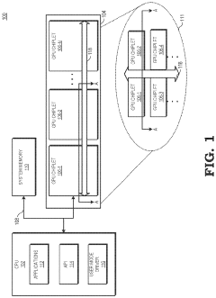
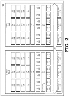
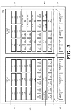
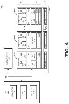
GPU chiplets using high bandwidth crosslinks
PatentWO2020263952A1
Innovation
- The use of high bandwidth passive crosslinks to couple GPU chiplets, allowing for unified cache coherence across all chiplets and maintaining a coherent view of memory, while preserving the current programming model by routing memory access requests through a passive interposer die.
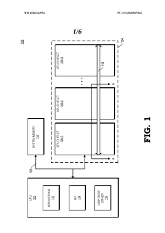
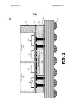
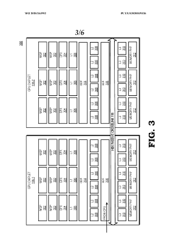
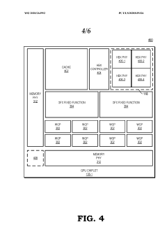
Non-homogeneous chiplets
PatentActiveUS12013810B2
Innovation
- The implementation of a semiconductor module with multiple interconnected GPU chiplets, each with a common set of circuitry modules and non-homogeneous supporting modules, allows for efficient distribution of workloads across chiplets, utilizing an interconnect that provides coherent memory access and routes commands to appropriate chiplets based on their specific capabilities.
Standardization Efforts
Standardization efforts play a crucial role in the expansion of the Chiplet ecosystem, addressing both opportunities and challenges in this rapidly evolving field. As the industry moves towards disaggregated chip designs, the need for common interfaces and protocols becomes increasingly important to ensure interoperability and foster innovation.
Several industry consortia and standards organizations have emerged to tackle the standardization challenges in the Chiplet ecosystem. The Universal Chiplet Interconnect Express (UCIe) consortium, formed in 2022, has been at the forefront of these efforts. UCIe aims to establish a universal interconnect standard for Chiplets, enabling seamless integration of components from different vendors.
The UCIe specification defines both the physical layer and protocol layer for die-to-die interconnects. It covers aspects such as electrical signaling, power delivery, and thermal management. By providing a common framework, UCIe facilitates the development of a diverse ecosystem of Chiplet components that can be mixed and matched to create custom system-on-chip (SoC) designs.
Another significant standardization effort is the Open Compute Project's (OCP) Chiplet Design Exchange (CDX) format. CDX aims to standardize the way Chiplet designs are described and exchanged between different tools and vendors. This initiative addresses the challenge of design interoperability, enabling more efficient collaboration and reducing time-to-market for Chiplet-based products.
The JEDEC Solid State Technology Association has also been active in the Chiplet standardization space. Their focus has been on developing standards for memory interfaces and packaging technologies that are critical for Chiplet integration. These efforts complement the work of UCIe and OCP, addressing specific aspects of the Chiplet ecosystem.
While significant progress has been made in standardization, challenges remain. One key issue is the need for broader industry adoption of these standards. As more companies join the Chiplet ecosystem, ensuring compliance and compatibility across a diverse range of products becomes increasingly complex.
Another challenge lies in balancing the need for standardization with the desire for innovation. Standards must be flexible enough to accommodate future technological advancements while providing a stable foundation for current designs. This requires ongoing collaboration and regular updates to the standards as the Chiplet ecosystem evolves.
Looking ahead, standardization efforts are likely to expand into areas such as testing and verification protocols for Chiplet-based systems, as well as standards for advanced packaging technologies. These efforts will be crucial in realizing the full potential of Chiplet technology and driving its adoption across various industries.
Ecosystem Collaboration
The expansion of the chiplet ecosystem presents both significant opportunities and challenges for the semiconductor industry. Collaboration among various stakeholders is crucial for realizing the full potential of chiplet technology and overcoming the associated hurdles.
One of the primary opportunities in ecosystem collaboration is the potential for standardization. As more companies adopt chiplet-based designs, there is a growing need for industry-wide standards to ensure interoperability and compatibility between different chiplet components. Organizations such as the Universal Chiplet Interconnect Express (UCIe) consortium are working towards establishing common protocols and interfaces, which could accelerate chiplet adoption and foster innovation across the ecosystem.
Another key aspect of ecosystem collaboration is the development of advanced packaging technologies. Chiplet designs rely heavily on sophisticated packaging solutions to integrate multiple dies efficiently. Collaboration between chip designers, packaging companies, and equipment manufacturers is essential to drive advancements in areas such as 2.5D and 3D packaging, silicon interposers, and through-silicon vias (TSVs).
The chiplet ecosystem also offers opportunities for specialized companies to focus on their core competencies. For instance, some firms may concentrate on developing high-performance compute chiplets, while others may specialize in memory or I/O chiplets. This specialization can lead to more efficient resource allocation and faster innovation cycles within the industry.
However, ecosystem collaboration also faces several challenges. One significant hurdle is the need for seamless integration between different chiplet components. Ensuring that chiplets from various vendors can work together harmoniously requires extensive collaboration and testing, which can be time-consuming and resource-intensive.
Intellectual property (IP) management is another critical challenge in the chiplet ecosystem. As multiple companies contribute to a single chiplet-based product, clear agreements on IP ownership, licensing, and royalties become essential. Establishing fair and transparent IP frameworks that encourage innovation while protecting individual contributions is crucial for sustained ecosystem growth.
Furthermore, the chiplet ecosystem must address supply chain complexities. Coordinating the production and delivery of multiple chiplet components from different suppliers requires sophisticated logistics and inventory management. Collaboration between foundries, outsourced semiconductor assembly and test (OSAT) providers, and system integrators is vital to ensure smooth production flows and minimize disruptions.
In conclusion, the expansion of the chiplet ecosystem offers tremendous opportunities for innovation and specialization. However, realizing these benefits requires overcoming significant challenges through collaborative efforts in standardization, advanced packaging, IP management, and supply chain optimization. As the ecosystem continues to evolve, strong partnerships and industry-wide cooperation will be key to unlocking the full potential of chiplet technology.
Unlock deeper insights with PatSnap Eureka Quick Research — get a full tech report to explore trends and direct your research. Try now!
Generate Your Research Report Instantly with AI Agent
Supercharge your innovation with PatSnap Eureka AI Agent Platform!