

Chiplet Evolution: Key Milestones and Future Insights
JUL 16, 20259 MIN READ
Generate Your Research Report Instantly with AI Agent
PatSnap Eureka helps you evaluate technical feasibility & market potential.
Chiplet Background and Objectives
Chiplets have emerged as a revolutionary approach in semiconductor design and manufacturing, addressing the challenges posed by Moore's Law and the increasing complexity of integrated circuits. This technology represents a paradigm shift from traditional monolithic chip designs to a modular approach, where multiple smaller dies, or "chiplets," are integrated onto a single package.
The evolution of chiplets can be traced back to the early 2000s when the concept of multi-chip modules (MCMs) gained traction. However, it wasn't until the mid-2010s that chiplets began to gain significant momentum in the industry. The primary driving force behind this shift was the need to overcome the limitations of traditional chip scaling and the rising costs associated with advanced process nodes.
As transistor sizes approached physical limits, chiplets offered a way to continue improving performance and functionality without relying solely on node shrinkage. This approach allows manufacturers to mix and match different process technologies, optimizing each chiplet for its specific function while maintaining overall system performance and cost-effectiveness.
The objectives of chiplet technology are multifaceted. Firstly, it aims to enhance performance by allowing the integration of specialized components optimized for specific tasks. This modular approach enables the combination of high-performance cores with power-efficient ones, or the integration of memory and logic on the same package, leading to improved overall system performance.
Secondly, chiplets address the escalating costs associated with advanced process nodes. By allowing the use of mature process nodes for less critical components while reserving cutting-edge processes for performance-critical parts, chiplets offer a more cost-effective solution for complex system-on-chip (SoC) designs.
Another key objective is to improve yield and reduce waste in semiconductor manufacturing. With monolithic designs, a single defect can render an entire large chip unusable. Chiplets mitigate this risk by allowing manufacturers to produce smaller, individual components with higher yield rates and then integrate them into a final package.
Chiplet technology also aims to accelerate time-to-market for new products. The modular nature of chiplets enables faster design iterations and more flexible product development cycles. Companies can reuse existing chiplet designs across multiple products, reducing development time and costs.
Looking ahead, the chiplet approach is expected to play a crucial role in advancing fields such as artificial intelligence, high-performance computing, and 5G/6G communications. As the technology matures, industry standards for chiplet interfaces and integration methodologies are being developed to foster wider adoption and interoperability across different manufacturers and design ecosystems.
Market Demand Analysis
The market demand for chiplet technology has been experiencing significant growth, driven by the increasing need for high-performance computing solutions across various industries. As traditional monolithic chip designs approach their physical limits, chiplets offer a promising alternative to continue scaling performance and functionality while managing costs and manufacturing complexity.
In the data center and cloud computing sector, the demand for chiplets is particularly strong. Major cloud service providers and hyperscalers are constantly seeking ways to improve their server performance and energy efficiency. Chiplets allow for more flexible and customizable designs, enabling these companies to optimize their hardware for specific workloads and reduce overall power consumption.
The telecommunications industry, especially with the ongoing rollout of 5G networks, is another key driver of chiplet demand. The need for high-performance, low-latency processing in base stations and network equipment aligns well with the advantages offered by chiplet-based designs. As 5G infrastructure continues to expand globally, the market for chiplets in this sector is expected to grow substantially.
In the consumer electronics market, chiplets are gaining traction in high-end devices such as gaming consoles, smartphones, and laptops. These products require increasingly powerful processors and graphics capabilities, which can be more efficiently delivered through chiplet-based architectures. The ability to mix and match different chiplets also allows manufacturers to create more diverse product lines and target specific market segments more effectively.
The automotive industry is emerging as a significant potential market for chiplets. As vehicles become more autonomous and connected, the demand for advanced computing power in automobiles is rising rapidly. Chiplets offer a scalable solution for implementing complex AI and sensor fusion algorithms required for autonomous driving systems, as well as for enhancing in-vehicle infotainment and connectivity features.
Looking at market trends, the adoption of chiplet technology is expected to accelerate in the coming years. This growth is fueled by the increasing complexity of semiconductor designs and the need for more specialized computing solutions. The chiplet market is projected to expand across various applications, including high-performance computing, edge computing, and AI accelerators.
However, challenges remain in standardization and interoperability between different chiplet designs. Industry initiatives like the Universal Chiplet Interconnect Express (UCIe) consortium are working to address these issues, which could further boost market adoption and expand the ecosystem of chiplet-based products.
Chiplet Technology Status
Chiplet technology has emerged as a revolutionary approach in semiconductor design and manufacturing, addressing the challenges of traditional monolithic chip designs. The current status of chiplet technology reflects significant advancements and widespread adoption across the industry.
Major semiconductor companies, including AMD, Intel, and TSMC, have embraced chiplet architecture in their product lines. AMD's Zen-based processors utilize chiplets to achieve high core counts and performance scalability. Intel's Foveros 3D packaging technology enables the integration of diverse chiplets in a single package. TSMC offers advanced packaging solutions like Chip-on-Wafer-on-Substrate (CoWoS) and Integrated Fan-Out (InFO) to support chiplet-based designs.
The adoption of chiplets has led to improved yield rates and cost-effectiveness in chip production. By manufacturing smaller, less complex chiplets separately and then integrating them, companies can achieve higher yields and reduce overall production costs. This approach also allows for greater flexibility in mixing and matching different process nodes within a single package.
Interconnect technologies play a crucial role in chiplet implementation. Advanced interconnect standards like Universal Chiplet Interconnect Express (UCIe) are being developed to ensure interoperability between chiplets from different vendors. These standards aim to create an open ecosystem for chiplet-based designs, fostering innovation and competition.
Power efficiency and thermal management remain key focus areas in chiplet technology. Advanced packaging techniques, such as 2.5D and 3D integration, are being employed to optimize power delivery and heat dissipation in multi-chiplet designs. These techniques enable the creation of high-performance, energy-efficient systems that were previously unattainable with monolithic designs.
The chiplet approach has also facilitated the development of heterogeneous computing architectures. By combining chiplets with different functionalities, such as CPUs, GPUs, and AI accelerators, manufacturers can create highly specialized and efficient systems tailored to specific applications.
However, challenges persist in chiplet technology. Die-to-die communication bandwidth and latency remain areas of ongoing research and development. Ensuring consistent performance across different chiplets and managing the complexity of multi-chiplet designs also present significant engineering challenges.
As the semiconductor industry continues to push the boundaries of Moore's Law, chiplet technology is poised to play an increasingly important role in future chip designs. The ongoing development of advanced packaging technologies, interconnect standards, and design tools is expected to further enhance the capabilities and adoption of chiplet-based architectures across a wide range of applications.
Current Chiplet Solutions
01 Chiplet architecture and integration
Chiplets are modular components that can be integrated to form larger, more complex systems-on-chip. This approach allows for flexible design, improved yield, and cost-effective manufacturing of advanced semiconductor devices. The integration of chiplets often involves advanced packaging technologies and interconnect solutions to ensure high-performance communication between different chiplet modules.- Chiplet architecture and integration: Chiplets are modular components that can be integrated to form larger, more complex systems-on-chip. This approach allows for flexible design, improved performance, and cost-effective manufacturing. The architecture involves connecting multiple smaller dies or chiplets using advanced packaging technologies, enabling the creation of customized solutions for various applications.
- Interconnect technologies for chiplets: Various interconnect technologies are employed to facilitate communication between chiplets and ensure efficient data transfer. These may include advanced packaging techniques, through-silicon vias (TSVs), interposers, and high-bandwidth interfaces. The choice of interconnect technology impacts the overall performance, power consumption, and thermal management of the chiplet-based system.
- Power management in chiplet designs: Effective power management is crucial in chiplet-based systems to optimize performance and energy efficiency. This involves implementing advanced power gating techniques, voltage scaling, and thermal management strategies across multiple chiplets. Intelligent power distribution and control mechanisms are employed to balance the power consumption of individual chiplets and the overall system.
- Testing and validation of chiplet-based systems: Ensuring the reliability and functionality of chiplet-based systems requires comprehensive testing and validation procedures. This includes developing specialized test methodologies for individual chiplets, as well as integrated system-level testing. Advanced diagnostic tools and techniques are employed to identify and isolate potential issues in the complex chiplet ecosystem.
- Chiplet standardization and interoperability: Efforts are underway to establish industry standards for chiplet designs and interfaces, promoting interoperability and ecosystem growth. This includes defining common protocols, electrical and physical specifications, and design methodologies. Standardization aims to facilitate the integration of chiplets from different vendors and enable a more diverse and competitive chiplet marketplace.
02 Interconnect technologies for chiplets
Various interconnect technologies are employed to facilitate high-bandwidth, low-latency communication between chiplets. These may include advanced packaging solutions, through-silicon vias (TSVs), interposers, and novel interconnect fabrics. The choice of interconnect technology significantly impacts the overall performance, power efficiency, and thermal management of chiplet-based systems.Expand Specific Solutions03 Power management and thermal solutions for chiplet designs
Effective power management and thermal solutions are crucial for chiplet-based systems. This includes innovative cooling techniques, power gating strategies, and dynamic voltage and frequency scaling (DVFS) methods tailored for multi-chiplet architectures. These solutions aim to optimize energy efficiency and maintain thermal stability across the integrated chiplet system.Expand Specific Solutions04 Testing and validation of chiplet-based systems
Specialized testing and validation methodologies are developed for chiplet-based systems to ensure functionality, performance, and reliability. This includes pre-integration testing of individual chiplets, interface testing between chiplets, and system-level validation of the integrated solution. Advanced testing techniques may involve built-in self-test (BIST) mechanisms and machine learning-based approaches for fault detection and diagnosis.Expand Specific Solutions05 Chiplet standardization and ecosystem development
Efforts are underway to establish industry standards for chiplet interfaces, packaging, and integration methodologies. This standardization aims to create a robust ecosystem that enables interoperability between chiplets from different vendors, fostering innovation and reducing time-to-market for chiplet-based products. The development of open chiplet platforms and design tools supports this ecosystem growth.Expand Specific Solutions
Key Players in Chiplet Industry
The chiplet evolution landscape is characterized by intense competition and rapid technological advancements. The market is in a growth phase, with major players like TSMC, Intel, and Huawei investing heavily in chiplet technology. Market size is expanding as chiplets offer improved performance and cost-effectiveness in various applications. Technological maturity varies among companies, with leaders like TSMC and Intel demonstrating advanced capabilities in chiplet design and integration. Emerging players such as Huawei and Qualcomm are also making significant strides, while research institutions like ICT-CAS and universities contribute to innovation. The competitive landscape is dynamic, with companies racing to develop more efficient and versatile chiplet solutions for next-generation computing systems.
Taiwan Semiconductor Manufacturing Co., Ltd.
Technical Solution: TSMC has made significant strides in chiplet technology with its 3DFabric architecture. This platform integrates front-end technologies like SoIC (System on Integrated Chips) for chip stacking and CoWoS (Chip on Wafer on Substrate) for 2.5D integration[4]. TSMC's approach allows for the combination of various process nodes and IP blocks, enabling customers to create highly customized and efficient designs. The company has also developed its InFO (Integrated Fan-Out) packaging technology, which has been crucial for advanced mobile processors[5]. TSMC's commitment to pushing the boundaries of process nodes, currently at 3nm with plans for 2nm and beyond, provides a solid foundation for future chiplet innovations[6].
Strengths: Industry-leading process nodes, diverse packaging technologies, and strong partnerships with major chip designers. Weaknesses: High capital expenditure requirements and geopolitical risks.
Intel Corp.
Technical Solution: Intel has been at the forefront of chiplet evolution with its Foveros 3D packaging technology. This approach allows for the vertical stacking of chiplets, enabling higher performance and lower power consumption. Intel's latest advancements include Foveros Omni and Foveros Direct, which offer even greater flexibility in chip design and improved interconnects[1]. The company has also introduced its Intel 20A and 18A process nodes, which incorporate RibbonFET and PowerVia technologies, further enhancing chiplet performance and efficiency[2]. Intel's chiplet strategy extends to its Ponte Vecchio GPU, which utilizes over 40 tiles manufactured on different process nodes, demonstrating the scalability and versatility of their chiplet approach[3].
Strengths: Advanced 3D packaging technology, diverse manufacturing capabilities, and extensive R&D resources. Weaknesses: Delays in process node advancements and competition from specialized chipmakers.
Core Chiplet Innovations
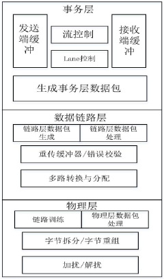
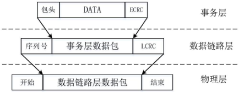
Data transmission system suitable for aerospace chiplet interconnection protocol
PatentPendingCN117331881A
Innovation
- Design a data transmission system suitable for aerospace chiplet interconnection protocols, including the transaction layer, data link layer and physical layer. It realizes high-speed data transmission through the arbiter, uses CRC checksum error correction mechanism to enhance reliability, and converts multi-bit parallelism. The data is serial data and is transmitted at high speed through the serial interface.
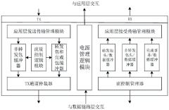
High-reliability Chiplet packaging structure based on adapter plate
PatentPendingCN117316917A
Innovation
- Adopt a high-reliability chiplet packaging structure based on the adapter board, through the first solder ball connection between the package substrate and the adapter board, the second solder ball connection between the adapter board and the bare chip, and on the adapter board Conductive holes are provided for electrical connection, and adhesive glue is used on the edge area of the adapter board to provide structural support and stress relief.


Chiplet Ecosystem Development
The chiplet ecosystem has undergone significant development in recent years, driven by the need for more efficient and scalable semiconductor solutions. This evolution has been marked by collaborative efforts among various industry players, including chip designers, manufacturers, and packaging specialists.
Initially, the chiplet approach was primarily explored by a few leading companies, with AMD's Zen architecture being one of the early adopters. As the benefits of chiplets became more apparent, other major players like Intel and TSMC began investing heavily in this technology, expanding the ecosystem's reach and capabilities.
A crucial milestone in the chiplet ecosystem's development was the establishment of industry standards. The formation of the Universal Chiplet Interconnect Express (UCIe) consortium in 2022 marked a significant step towards interoperability. This initiative, supported by industry giants such as Intel, AMD, Arm, TSMC, and Samsung, aims to create a unified standard for die-to-die interconnects, facilitating easier integration of chiplets from different vendors.
The ecosystem has also seen advancements in packaging technologies, which are essential for chiplet implementation. Innovations in 2.5D and 3D packaging, such as TSMC's CoWoS (Chip on Wafer on Substrate) and Intel's EMIB (Embedded Multi-die Interconnect Bridge), have enabled more sophisticated chiplet designs and improved performance.
Another key aspect of the ecosystem's growth has been the development of specialized IP and design tools. EDA companies have introduced new software solutions tailored for chiplet-based designs, addressing challenges in system-level integration and optimization. Additionally, IP providers have begun offering chiplet-specific solutions, such as die-to-die interfaces and PHY designs.
The chiplet ecosystem has also expanded to include specialized foundries and OSATs (Outsourced Semiconductor Assembly and Test) providers. These companies play a crucial role in manufacturing and packaging chiplets, offering services that enable smaller companies to leverage chiplet technology without massive infrastructure investments.
Looking ahead, the chiplet ecosystem is poised for further growth and diversification. Emerging technologies like silicon photonics for chip-to-chip communication and advanced cooling solutions for high-density chiplet designs are expected to drive the next phase of innovation. Moreover, the ecosystem is likely to see increased specialization, with companies focusing on niche areas such as specific types of chiplets or advanced packaging solutions.
Chiplet Standardization Efforts
Chiplet standardization efforts have become a crucial aspect of the semiconductor industry's evolution towards more modular and flexible chip designs. These initiatives aim to establish common protocols, interfaces, and design methodologies that enable seamless integration of diverse chiplets from multiple vendors.
One of the most significant standardization efforts is the Universal Chiplet Interconnect Express (UCIe) consortium, formed in 2022. UCIe brings together major industry players like Intel, AMD, Arm, TSMC, and Samsung to develop an open specification for die-to-die interconnects. This standard focuses on defining physical and protocol layers for chiplet communication, promoting interoperability and reducing design complexity.
Another important initiative is the Open Compute Project's (OCP) Chiplet Design Exchange (CDX) working group. CDX aims to create an open ecosystem for chiplet-based designs, focusing on standardizing chiplet interfaces, packaging, and testing methodologies. This effort complements UCIe by addressing broader aspects of chiplet integration and manufacturing.
The CHIPS Alliance, an open-source hardware organization, has also been actively working on chiplet standardization. Their efforts include developing open-source tools and IP for chiplet-based designs, as well as promoting standardization of chiplet interfaces and packaging technologies.
In parallel, the IEEE has been developing standards related to chiplet integration, such as IEEE P2851 for chiplet security and IEEE P3079 for 3D system integration. These standards address specific aspects of chiplet technology, contributing to a more comprehensive standardization landscape.
The JEDEC Solid State Technology Association has also been involved in chiplet standardization, particularly in the area of memory integration. Their efforts focus on standardizing interfaces between logic and memory chiplets, which is crucial for enabling high-bandwidth, low-power memory solutions in chiplet-based designs.
As chiplet technology continues to evolve, these standardization efforts are expected to expand and refine. Future focus areas may include advanced packaging technologies, thermal management standards, and security protocols specific to chiplet-based systems. The success of these initiatives will be critical in realizing the full potential of chiplet technology, enabling a more diverse and innovative semiconductor ecosystem.
Unlock deeper insights with PatSnap Eureka Quick Research — get a full tech report to explore trends and direct your research. Try now!
Generate Your Research Report Instantly with AI Agent
Supercharge your innovation with PatSnap Eureka AI Agent Platform!