Chiplet Integration in Evolving Digital Scenario Models
JUL 16, 202510 MIN READ
Generate Your Research Report Instantly with AI Agent
Patsnap Eureka helps you evaluate technical feasibility & market potential.
Chiplet Integration Background and Objectives
Chiplet integration has emerged as a transformative approach in the semiconductor industry, addressing the challenges posed by the slowing of Moore's Law and the increasing complexity of system-on-chip (SoC) designs. This technology allows for the disaggregation of large, monolithic dies into smaller, more manageable chiplets, which can be manufactured separately and then integrated onto a single package.
The evolution of chiplet integration can be traced back to the early 2010s when the concept began to gain traction among leading semiconductor companies. Initially driven by the need to improve yield and reduce costs in high-performance computing applications, chiplet technology has since expanded its scope to encompass a wide range of digital scenarios, including artificial intelligence, edge computing, and 5G infrastructure.
As digital scenario models continue to evolve, chiplet integration has become increasingly crucial in meeting the demands for higher performance, lower power consumption, and improved scalability. The technology enables the combination of heterogeneous components, each optimized for specific functions, onto a single package. This modular approach not only enhances overall system performance but also provides greater flexibility in design and manufacturing processes.
The primary objectives of chiplet integration in evolving digital scenario models are multifaceted. Firstly, it aims to overcome the limitations of traditional monolithic chip designs by enabling the use of different process nodes for various components, thereby optimizing performance and cost. Secondly, chiplet integration seeks to improve yield rates by allowing manufacturers to produce smaller, less complex dies with higher success rates.
Furthermore, chiplet technology targets enhanced scalability and customization capabilities, enabling system designers to mix and match different chiplets to create tailored solutions for specific applications. This flexibility is particularly valuable in the rapidly changing landscape of digital scenarios, where adaptability and rapid time-to-market are critical factors.
Another key objective is to facilitate the integration of specialized accelerators and IP blocks from different vendors, fostering innovation and competition in the semiconductor ecosystem. This open approach to chip design has the potential to democratize access to advanced semiconductor technologies and drive down costs across the industry.
As digital scenarios continue to evolve, chiplet integration also aims to address the growing concerns around power efficiency and thermal management in complex systems. By optimizing the placement and interconnection of chiplets, designers can achieve better power distribution and heat dissipation, leading to more energy-efficient and reliable products.
In conclusion, the background and objectives of chiplet integration in evolving digital scenario models reflect a paradigm shift in semiconductor design and manufacturing. This technology represents a strategic response to the challenges faced by the industry, offering a path forward for continued innovation and performance improvements in an era where traditional scaling approaches are reaching their limits.
Market Demand Analysis for Chiplet Solutions
The market demand for chiplet solutions in evolving digital scenario models has been experiencing significant growth, driven by the increasing complexity of modern computing systems and the need for more efficient, scalable, and cost-effective semiconductor designs. As traditional monolithic chip designs reach their physical and economic limits, chiplets offer a promising alternative that allows for modular integration of different functional components.
The demand for chiplet solutions is particularly strong in data centers and high-performance computing environments, where the need for processing power and energy efficiency continues to grow exponentially. These sectors require advanced computing capabilities to handle complex workloads such as artificial intelligence, machine learning, and big data analytics. Chiplet-based designs enable the integration of specialized processing units, memory modules, and I/O interfaces, allowing for customized solutions that can be tailored to specific application requirements.
In the telecommunications industry, the rollout of 5G networks and the development of 6G technologies are creating new opportunities for chiplet integration. The demand for high-bandwidth, low-latency communication systems is driving the need for more sophisticated and flexible chip designs. Chiplets offer the potential to combine different radio frequency (RF) components, baseband processors, and network processors on a single package, enabling more compact and efficient network equipment.
The automotive sector is another key market for chiplet solutions, as vehicles become increasingly connected and autonomous. Advanced driver assistance systems (ADAS) and in-vehicle infotainment systems require powerful, energy-efficient computing platforms that can be easily updated and scaled. Chiplet-based designs allow for the integration of various sensors, processors, and communication modules, providing the flexibility needed to meet evolving automotive requirements.
Consumer electronics, including smartphones, tablets, and wearable devices, represent a growing market for chiplet solutions. As these devices incorporate more advanced features such as AI-powered cameras, augmented reality capabilities, and improved battery life, chiplet integration offers a way to pack more functionality into smaller form factors while maintaining power efficiency.
The industrial Internet of Things (IIoT) and edge computing applications are also driving demand for chiplet solutions. These sectors require robust, low-power computing platforms that can operate in harsh environments and process data locally. Chiplet-based designs enable the creation of modular, scalable systems that can be easily adapted to different industrial use cases.
As the market for chiplet solutions continues to expand, there is a growing need for standardization and ecosystem development. Industry collaborations and initiatives are emerging to address challenges related to chiplet integration, including interface standards, packaging technologies, and design methodologies. This ecosystem development is crucial for accelerating the adoption of chiplet-based designs across various market segments and ensuring interoperability between different chiplet solutions.
Chiplet Technology Status and Challenges
Chiplet technology has emerged as a revolutionary approach in the semiconductor industry, offering a paradigm shift in chip design and manufacturing. The current status of chiplet integration in evolving digital scenario models is characterized by significant advancements and persistent challenges.
The semiconductor industry has made substantial progress in chiplet technology, with major players like AMD, Intel, and TSMC leading the charge. These companies have successfully implemented chiplet-based designs in their high-performance processors and data center chips. The adoption of chiplets has enabled the creation of more complex and powerful systems while mitigating some of the challenges associated with monolithic chip designs.
One of the primary advantages of chiplet technology is its ability to overcome the limitations of traditional Moore's Law scaling. By disaggregating complex systems into smaller, more manageable components, chiplets allow for better yield management and cost-effective integration of heterogeneous technologies. This approach has proven particularly beneficial in the development of advanced computing systems for evolving digital scenarios, such as artificial intelligence, edge computing, and 5G networks.
However, despite these advancements, chiplet integration faces several significant challenges. One of the most pressing issues is the need for standardization in chiplet interfaces and protocols. The lack of industry-wide standards hampers interoperability between chiplets from different manufacturers, limiting the potential for a truly modular and flexible ecosystem.
Another major challenge lies in the realm of thermal management and power distribution. As chiplets enable the integration of diverse components with varying power requirements, ensuring efficient heat dissipation and power delivery across the entire system becomes increasingly complex. This challenge is particularly acute in high-performance computing applications where power density and thermal constraints are critical factors.
The integration of chiplets also presents challenges in terms of signal integrity and communication bandwidth. As the number of interconnects between chiplets increases, managing signal quality and minimizing latency becomes more difficult. This issue is exacerbated in scenarios requiring high-speed data transfer between multiple chiplets, such as in advanced AI accelerators or network processors.
Furthermore, the design and verification process for chiplet-based systems is significantly more complex than traditional monolithic designs. Engineers must contend with a multitude of variables, including die-to-die variations, packaging constraints, and system-level optimizations. This complexity necessitates the development of new design tools and methodologies specifically tailored for chiplet integration.
In the context of evolving digital scenario models, chiplet technology also faces challenges related to security and reliability. As systems become more modular and distributed, ensuring data integrity and protecting against potential vulnerabilities across multiple chiplets becomes increasingly important. This is particularly crucial in applications such as autonomous vehicles, industrial IoT, and secure edge computing, where system reliability and security are paramount.
Current Chiplet Integration Approaches
01 Digital scenario modeling for chiplet integration
This approach involves creating digital models to simulate and optimize chiplet integration scenarios. These models can help predict performance, power consumption, and thermal behavior of integrated chiplets, allowing designers to explore various configurations and optimize system-level performance before physical implementation.- Digital scenario modeling for chiplet integration: This approach involves creating digital models to simulate and optimize chiplet integration scenarios. These models help in predicting performance, power consumption, and thermal behavior of integrated chiplets, allowing for more efficient design and integration processes.
- AI-driven chiplet integration optimization: Artificial intelligence techniques are employed to optimize chiplet integration. Machine learning algorithms analyze various integration scenarios, predict outcomes, and suggest optimal configurations for improved performance and efficiency in multi-chip systems.
- Thermal management in chiplet integration: This focuses on developing digital models for thermal analysis and management in chiplet integration. The models simulate heat distribution and dissipation, helping to design better cooling solutions and optimize chiplet placement for thermal efficiency.
- Interconnect optimization for chiplet integration: Digital scenario models are used to optimize interconnect designs between chiplets. These models simulate various interconnect architectures, helping to reduce latency, improve bandwidth, and enhance overall system performance in multi-chip modules.
- Power distribution modeling for integrated chiplets: This involves creating digital models to analyze and optimize power distribution across integrated chiplets. The models help in designing efficient power delivery networks, reducing power consumption, and ensuring stable operation of multi-chip systems.
02 AI-assisted chiplet integration design
Artificial intelligence techniques are employed to enhance chiplet integration design processes. Machine learning algorithms can analyze vast amounts of data from previous designs and simulations to suggest optimal chiplet configurations, interconnect strategies, and predict potential integration challenges.Expand Specific Solutions03 Thermal management modeling for chiplet integration
This focuses on creating digital models to analyze and optimize thermal management in chiplet-based systems. These models simulate heat dissipation patterns, identify potential hotspots, and help design effective cooling solutions for integrated chiplets, ensuring optimal performance and reliability.Expand Specific Solutions04 Interconnect optimization for chiplet integration
Digital scenario models are used to optimize interconnect strategies between chiplets. These models simulate various interconnect technologies, such as silicon interposers or advanced packaging techniques, to determine the most efficient and cost-effective integration solutions for specific chiplet configurations.Expand Specific Solutions05 System-level performance modeling for chiplet-based designs
This approach involves creating comprehensive digital models that simulate the entire system-level performance of chiplet-based designs. These models account for interactions between multiple chiplets, memory subsystems, and I/O interfaces, allowing designers to optimize overall system performance, power efficiency, and functionality.Expand Specific Solutions
Key Players in Chiplet Ecosystem
The chiplet integration market in evolving digital scenario models is in a growth phase, driven by increasing demand for high-performance computing and AI applications. The market size is expanding rapidly, with major players like Intel, TSMC, and AMD investing heavily in this technology. The technical maturity varies among companies, with established semiconductor giants like TSMC and Intel leading in advanced packaging techniques. Emerging players such as D-Matrix and MemryX are focusing on specialized AI chiplet solutions, while traditional IT companies like IBM and Huawei are also entering the space. The competitive landscape is dynamic, with companies racing to develop more efficient and scalable chiplet integration technologies to address the growing complexity of modern computing systems.
Intel Corp.
Technical Solution: Intel's approach to Chiplet Integration in Evolving Digital Scenario Models focuses on their Foveros 3D packaging technology. This advanced packaging solution allows for the vertical stacking of multiple chiplets, enabling higher performance and lower power consumption in a smaller form factor[1]. Intel's Foveros technology utilizes through-silicon vias (TSVs) and micro-bumps to connect different chiplets, allowing for the integration of heterogeneous components such as CPUs, GPUs, and memory[2]. The company has also introduced Embedded Multi-die Interconnect Bridge (EMIB) technology, which provides high-bandwidth connections between chiplets in a 2.5D configuration, further enhancing the flexibility of chiplet integration[3].
Strengths: Advanced 3D packaging technology, high-bandwidth interconnects, and flexibility in integrating heterogeneous components. Weaknesses: Potential thermal management challenges in 3D stacked designs and higher manufacturing complexity.
Huawei Technologies Co., Ltd.
Technical Solution: Huawei's approach to Chiplet Integration in Evolving Digital Scenario Models centers around their Kirin series of SoCs and custom AI accelerators. The company has been developing advanced packaging technologies to integrate multiple chiplets, including their proprietary Da Vinci AI cores, into a single package[4]. Huawei's chiplet strategy focuses on modular design, allowing for the combination of different functional blocks to create customized solutions for various applications, from smartphones to data centers[5]. They have also been investing in advanced 2.5D and 3D packaging technologies to improve interconnect density and reduce power consumption between chiplets[6].
Strengths: Strong focus on AI acceleration, modular design approach, and in-house development of advanced packaging technologies. Weaknesses: Geopolitical challenges affecting access to certain technologies and potential supply chain disruptions.
Core Innovations in Chiplet Technology
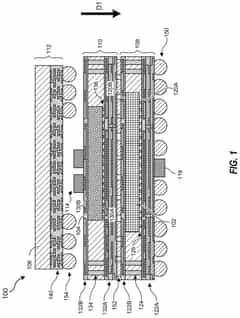
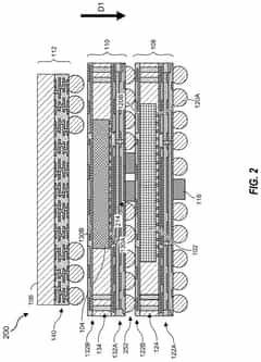
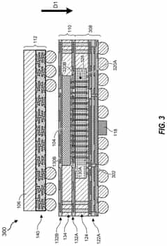
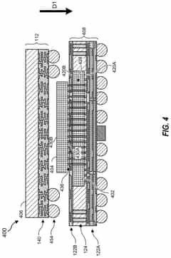
3D chiplet integration using fan-out wafer-level packaging
PatentPendingUS20240274587A1
Innovation
- The use of fan-out wafer-level packaging and three-dimensional packaging techniques for combining semiconductor chips and embedded memory in configurations such as face-to-back, back-to-back, and face-to-face orientations, enabling direct connections between chiplets and reducing assembly package sizes and manufacturing complexity.
Self-scheduling threads in a programmable atomic unit
PatentPendingUS20240086200A1
Innovation
- Implementing self-scheduling threads by using thread identifiers and a thread ready-to-run queue, where only threads without resource contention are executed, and thread IDs are removed and re-enqueued based on memory request completion, eliminating the need for traditional hazard tracking mechanisms.


Standardization Efforts in Chiplet Ecosystem
The standardization efforts in the chiplet ecosystem are crucial for ensuring interoperability and fostering innovation in the rapidly evolving field of chiplet integration. As the industry moves towards more modular and heterogeneous chip designs, the need for common standards and protocols becomes increasingly important.
One of the key initiatives in this area is the Universal Chiplet Interconnect Express (UCIe) consortium, which aims to establish a unified interconnect standard for chiplets. UCIe focuses on creating specifications for die-to-die interconnects, allowing chiplets from different vendors to communicate seamlessly. This standard addresses physical layer, protocol layer, and software layer considerations, providing a comprehensive framework for chiplet integration.
Another significant standardization effort is the Open Compute Project's (OCP) Chiplet Design Exchange (CDX) format. CDX aims to create a common language for describing chiplet designs, facilitating easier collaboration between different companies and design teams. This format includes specifications for physical design, electrical characteristics, and thermal properties of chiplets.
The JEDEC Solid State Technology Association has also been active in developing standards for chiplet-based systems. Their focus includes memory interface standards and thermal management guidelines for multi-chip modules, which are essential for ensuring reliable performance in chiplet-based designs.
In addition to these industry-led initiatives, government agencies and research institutions are also contributing to standardization efforts. For instance, the DARPA CHIPS (Common Heterogeneous Integration and IP Reuse Strategies) program has been instrumental in promoting modular chip design and standardization of chiplet interfaces.
The IEEE has formed working groups to address various aspects of chiplet integration, including the IEEE P2851 standard for 3D stacked integrated circuits. This standard aims to define test access mechanisms and design-for-test methodologies specific to 3D integrated circuits, which are closely related to chiplet-based designs.
Standardization efforts also extend to packaging technologies, with organizations like SEMI developing standards for advanced packaging processes and materials. These standards are crucial for ensuring consistency and reliability in the manufacturing of chiplet-based systems.
As the chiplet ecosystem continues to evolve, ongoing collaboration between industry players, academia, and standards bodies will be essential. The success of these standardization efforts will play a pivotal role in accelerating the adoption of chiplet technology and enabling more flexible and efficient digital scenario models.
Thermal Management in Chiplet Designs
Thermal management is a critical aspect of chiplet designs, particularly as the integration of multiple chiplets in evolving digital scenario models becomes more prevalent. The increased power density and heat generation in these compact, high-performance systems pose significant challenges for maintaining optimal operating temperatures and ensuring reliable performance.
One of the primary thermal management strategies in chiplet designs involves the use of advanced packaging technologies. These include the implementation of through-silicon vias (TSVs) and interposers, which not only facilitate electrical connections between chiplets but also aid in heat dissipation. The strategic placement of TSVs can create thermal pathways that efficiently conduct heat away from high-temperature regions, distributing it more evenly across the package.
Another key approach is the incorporation of advanced thermal interface materials (TIMs) between chiplets and heat spreaders. These materials, such as indium-based alloys or phase-change materials, offer superior thermal conductivity compared to traditional thermal pastes. They help to minimize thermal resistance at interfaces, enabling more effective heat transfer from the chiplets to the cooling system.
Active cooling solutions play a crucial role in chiplet thermal management. Microfluidic cooling channels integrated within the interposer or substrate can provide localized cooling to high-heat-flux areas. These channels allow for the circulation of coolants in close proximity to the heat sources, offering significantly higher cooling capacity compared to traditional air cooling methods.
The design of the heat spreader and integrated heat sink is also critical in chiplet thermal management. Advanced designs may incorporate vapor chambers or heat pipes to efficiently spread heat across a larger surface area before it is dissipated to the ambient environment. The use of materials with high thermal conductivity, such as copper or graphene-based composites, further enhances the effectiveness of these components.
Thermal modeling and simulation tools are essential for optimizing the thermal design of chiplet-based systems. These tools allow engineers to predict hotspots, analyze thermal gradients, and evaluate the effectiveness of various cooling strategies before physical prototyping. Advanced thermal simulation software can account for the complex geometries and material properties of chiplet designs, enabling more accurate thermal predictions and design optimizations.
In conclusion, effective thermal management in chiplet designs requires a multi-faceted approach, combining advanced packaging technologies, innovative cooling solutions, and sophisticated thermal modeling. As chiplet integration continues to evolve in digital scenario models, the development of more efficient and targeted thermal management strategies will be crucial for realizing the full potential of these high-performance, modular computing architectures.
Unlock deeper insights with Patsnap Eureka Quick Research — get a full tech report to explore trends and direct your research. Try now!
Generate Your Research Report Instantly with AI Agent
Supercharge your innovation with Patsnap Eureka AI Agent Platform!