Chiplet Solutions for Overcoming Bandwidth Bottlenecks
JUL 16, 20259 MIN READ
Generate Your Research Report Instantly with AI Agent
PatSnap Eureka helps you evaluate technical feasibility & market potential.
Chiplet Tech Evolution
The evolution of chiplet technology represents a significant paradigm shift in semiconductor design and manufacturing. This approach emerged as a response to the increasing challenges faced by traditional monolithic chip designs, particularly in terms of scalability, yield, and cost-effectiveness.
In the early stages of chiplet development, the focus was primarily on disaggregating large, complex System-on-Chip (SoC) designs into smaller, more manageable components. This initial phase, which began in the mid-2010s, saw companies like AMD pioneering the use of chiplets in their CPU designs, notably with the introduction of the Zen 2 architecture in 2019.
As the technology matured, the industry witnessed a rapid expansion in the application of chiplets across various semiconductor domains. The evolution progressed from simple multi-chip modules to more sophisticated 2.5D and 3D integration techniques. This advancement allowed for the combination of heterogeneous dies manufactured using different process nodes, optimizing performance and cost.
A critical milestone in chiplet evolution was the development of high-bandwidth, low-latency interconnect technologies. These interconnects, such as AMD's Infinity Fabric and Intel's EMIB (Embedded Multi-die Interconnect Bridge), played a crucial role in overcoming the bandwidth bottlenecks associated with inter-die communication. The continuous improvement of these interconnect technologies has been fundamental in realizing the full potential of chiplet-based designs.
The industry has also witnessed significant progress in packaging technologies to support chiplet integration. Advanced packaging solutions like TSMC's CoWoS (Chip on Wafer on Substrate) and Intel's Foveros have enabled more efficient and compact chiplet arrangements, further enhancing performance and reducing power consumption.
More recently, the focus has shifted towards standardization efforts to promote interoperability between chiplets from different vendors. Initiatives like the Universal Chiplet Interconnect Express (UCIe) consortium aim to establish common interfaces and protocols, potentially revolutionizing the semiconductor supply chain and enabling a more modular approach to chip design.
Looking ahead, the chiplet technology roadmap is poised for further innovations. Research is ongoing in areas such as optical interconnects for even higher bandwidth capabilities, advanced cooling solutions for densely packed chiplets, and AI-assisted design tools for optimizing chiplet-based systems. These advancements are expected to push the boundaries of performance, efficiency, and scalability in next-generation computing systems.
Market Demand Analysis
The market demand for Chiplet solutions to overcome bandwidth bottlenecks has been growing rapidly in recent years, driven by the increasing complexity and performance requirements of modern computing systems. As traditional monolithic chip designs approach their physical limits, the industry is shifting towards more modular and scalable architectures.
The global semiconductor market, particularly in the high-performance computing (HPC) and data center segments, has shown a strong appetite for Chiplet-based solutions. This demand is fueled by the need for higher bandwidth, improved energy efficiency, and reduced manufacturing costs. Major tech companies and cloud service providers are actively seeking ways to enhance their data processing capabilities while managing power consumption and thermal issues.
In the HPC sector, the demand for Chiplet solutions is particularly pronounced. Research institutions, government agencies, and private enterprises require ever-increasing computational power for complex simulations, artificial intelligence, and big data analytics. The ability of Chiplet designs to offer customizable, high-performance solutions with improved yield and cost-effectiveness makes them highly attractive in this market segment.
The telecommunications industry, especially with the ongoing rollout of 5G networks and the anticipated 6G technology, represents another significant market for Chiplet solutions. The need for high-bandwidth, low-latency communication systems aligns well with the capabilities offered by Chiplet architectures.
Consumer electronics, including smartphones, tablets, and gaming consoles, are also driving demand for Chiplet solutions. As these devices become more powerful and feature-rich, manufacturers are looking for ways to improve performance without significantly increasing power consumption or device size.
The automotive industry, particularly in the development of autonomous vehicles and advanced driver assistance systems (ADAS), is emerging as a potential growth area for Chiplet technology. These applications require high-performance, energy-efficient computing solutions that can operate reliably in challenging environments.
Market analysts project substantial growth in the Chiplet market over the coming years. The increasing adoption of artificial intelligence and machine learning across various industries is expected to further boost demand for high-bandwidth, scalable computing solutions.
However, the market also faces challenges. The complexity of integrating multiple chiplets and ensuring interoperability between different vendors' components can be a barrier to adoption. Additionally, the need for standardization in Chiplet interfaces and packaging technologies is crucial for widespread market acceptance.
Bandwidth Bottlenecks
Bandwidth bottlenecks have become a critical challenge in modern computing systems, particularly as data processing demands continue to escalate. These bottlenecks occur when the rate at which data can be transferred between different components of a system is insufficient to meet the processing requirements. This limitation can significantly impact overall system performance, leading to reduced efficiency and increased latency.
The primary sources of bandwidth bottlenecks in computing systems are diverse and interconnected. Memory bandwidth, for instance, often becomes a limiting factor as processors struggle to access data from RAM quickly enough to maintain peak performance. Similarly, interconnect bandwidth between different processing units, such as CPUs and GPUs, can create bottlenecks that hinder the efficient exchange of data and instructions.
In data centers and high-performance computing environments, network bandwidth constraints can severely limit the speed at which information can be transferred between servers or storage systems. This issue is particularly pronounced in applications involving big data analytics, artificial intelligence, and scientific simulations, where massive amounts of data need to be moved and processed rapidly.
The impact of bandwidth bottlenecks extends beyond raw performance metrics. Energy efficiency is also affected, as systems may consume more power while waiting for data transfers to complete. Moreover, these bottlenecks can lead to increased complexity in software design, as developers must optimize their code to work around hardware limitations.
As technology advances, the demand for bandwidth continues to grow exponentially. This trend is driven by emerging applications such as 5G networks, edge computing, and the Internet of Things (IoT), which generate and process unprecedented volumes of data. The increasing adoption of AI and machine learning algorithms further exacerbates the bandwidth challenge, as these technologies often require rapid access to large datasets.
Addressing bandwidth bottlenecks requires a multifaceted approach, combining innovations in hardware design, system architecture, and software optimization. Emerging technologies such as high-bandwidth memory (HBM), silicon photonics, and advanced packaging techniques offer promising solutions to alleviate these constraints. However, the complexity of modern computing ecosystems necessitates holistic strategies that consider the entire data flow path, from storage to processing and back.
Current Chiplet Sols
01 High-bandwidth interconnects for chiplets
Advanced interconnect technologies are being developed to increase bandwidth between chiplets. These include high-speed SerDes, optical interconnects, and advanced packaging techniques that allow for denser connections between dies. These solutions aim to overcome bandwidth limitations in multi-chip modules and enable higher data transfer rates between chiplets.- High-bandwidth interconnects for chiplets: Advanced interconnect technologies are being developed to increase bandwidth between chiplets. These solutions include high-speed SerDes, optical interconnects, and advanced packaging techniques to reduce latency and improve data transfer rates between different chiplet components.
- Memory integration for improved bandwidth: Chiplet designs are incorporating advanced memory solutions, such as high-bandwidth memory (HBM) and on-chip caches, to reduce data access latency and increase overall system bandwidth. This integration allows for faster data transfer between processing elements and memory components.
- Network-on-Chip (NoC) architectures: Innovative Network-on-Chip architectures are being implemented in chiplet designs to optimize data movement and increase bandwidth. These architectures provide scalable and efficient communication between different chiplet components, improving overall system performance.
- Heterogeneous integration for bandwidth optimization: Chiplet solutions are leveraging heterogeneous integration techniques to combine different types of processors, accelerators, and I/O components. This approach allows for optimized bandwidth allocation based on specific workload requirements and improves overall system efficiency.
- Advanced packaging technologies for bandwidth enhancement: New packaging technologies, such as 2.5D and 3D integration, are being utilized to improve bandwidth in chiplet solutions. These technologies enable closer proximity between chiplets, reducing interconnect lengths and allowing for higher bandwidth connections between components.
02 Memory integration for improved bandwidth
Integrating high-bandwidth memory (HBM) or other advanced memory technologies directly with chiplets can significantly increase overall system bandwidth. This approach reduces latency and improves data transfer rates between processing elements and memory, enhancing performance in data-intensive applications.Expand Specific Solutions03 Network-on-Chip (NoC) architectures for chiplets
Implementing sophisticated Network-on-Chip architectures within chiplet designs can optimize data movement and increase effective bandwidth. These NoC designs can include advanced routing algorithms, quality-of-service features, and scalable topologies to efficiently manage communication between different functional blocks or chiplets.Expand Specific Solutions04 3D stacking and through-silicon vias (TSVs)
Utilizing 3D stacking technologies and through-silicon vias can significantly increase the bandwidth between chiplets by enabling vertical connections. This approach allows for shorter interconnects, reduced power consumption, and higher bandwidth density compared to traditional 2D arrangements.Expand Specific Solutions05 Adaptive and reconfigurable interconnects
Developing adaptive and reconfigurable interconnect solutions for chiplets can optimize bandwidth utilization based on workload demands. These systems can dynamically adjust data paths, clock rates, or power consumption to maximize efficiency and performance in varying operational conditions.Expand Specific Solutions
Key Chiplet Players
The chiplet solutions market for overcoming bandwidth bottlenecks is in a growth phase, with increasing adoption across the semiconductor industry. The market size is expanding rapidly as chiplet technology addresses scalability challenges in traditional monolithic chip designs. Technologically, chiplets are maturing, with key players like Intel, AMD, and TSMC making significant advancements. Intel's EMIB and Foveros technologies, along with AMD's Infinity Fabric, demonstrate the industry's progress. Other companies like Huawei, Samsung, and Fujitsu are also investing heavily in chiplet research and development, indicating a competitive and innovative landscape. As interconnect standards evolve and manufacturing processes improve, chiplet solutions are poised to become increasingly prevalent in high-performance computing and data-intensive applications.
Huawei Technologies Co., Ltd.
Technical Solution: Huawei's approach to Chiplet solutions for bandwidth bottlenecks involves their Kirin chip series and custom interconnect technologies. The company has developed a chiplet-based design for their Kirin processors, utilizing advanced packaging techniques to integrate multiple dies[1]. Huawei's solution includes a high-bandwidth, low-latency interconnect fabric that allows for efficient communication between chiplets[2]. They have also invested in 2.5D and 3D packaging technologies to optimize the integration of heterogeneous chiplets[3]. Huawei's chiplet strategy aims to improve performance, reduce power consumption, and enhance scalability in their mobile and AI processors[4]. The company has reportedly achieved data transfer rates of up to 4 Gbps between chiplets in their latest designs[5].
Strengths: Custom interconnect technology optimized for mobile and AI applications, vertical integration capabilities. Weaknesses: Potential limitations due to trade restrictions, less open ecosystem compared to some competitors.
Intel Corp.
Technical Solution: Intel's Chiplet solution for overcoming bandwidth bottlenecks focuses on their Embedded Multi-die Interconnect Bridge (EMIB) and Foveros 3D packaging technologies. EMIB uses a small silicon bridge embedded in the package substrate to connect multiple chiplets, providing high-bandwidth and low-latency connections[1]. Foveros enables vertical stacking of chiplets, allowing for even higher bandwidth density and shorter interconnects[2]. Intel has demonstrated these technologies in products like Ponte Vecchio, which combines multiple chiplets using both EMIB and Foveros to achieve over 5 petaFLOPS of compute performance[3]. The company has also introduced Advanced Interface Bus (AIB) as an open interconnect standard for chiplet-to-chiplet communication, supporting data rates up to 2 Gbps per pin[4].
Strengths: High bandwidth density, flexibility in chip design, and proven implementation in high-performance products. Weaknesses: Complexity in manufacturing and thermal management, potentially higher costs compared to monolithic designs.
Core Chiplet Patents
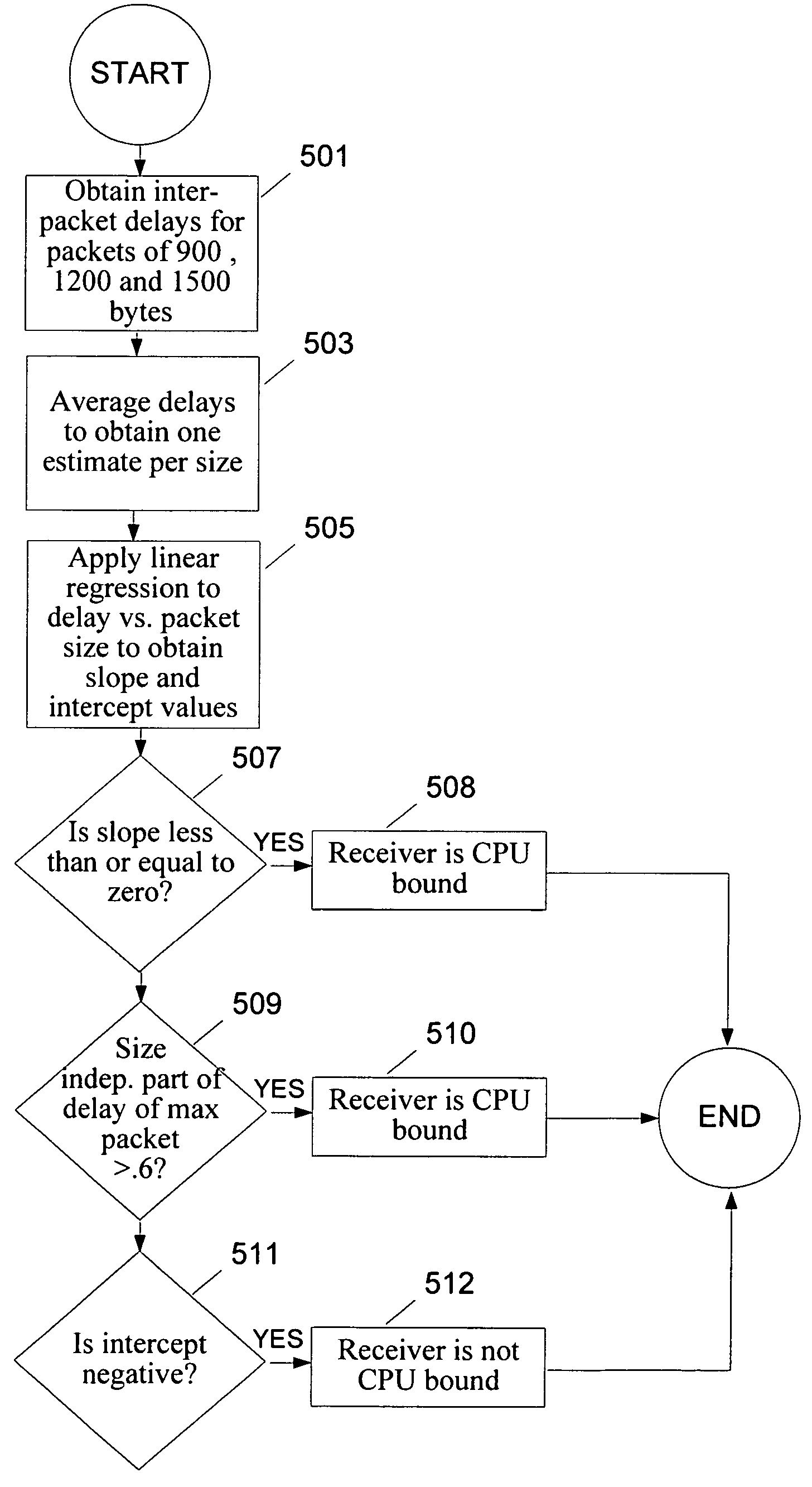
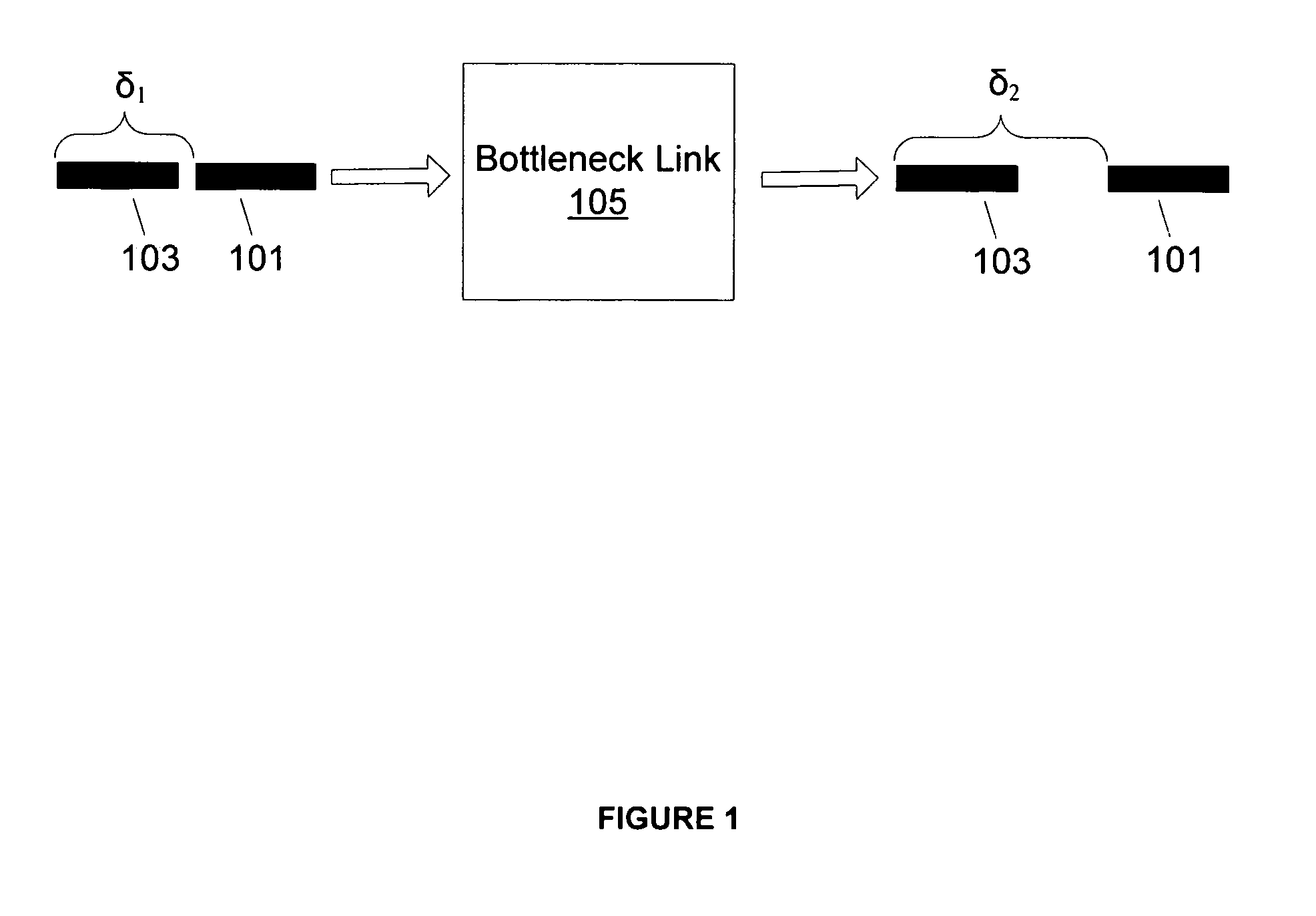
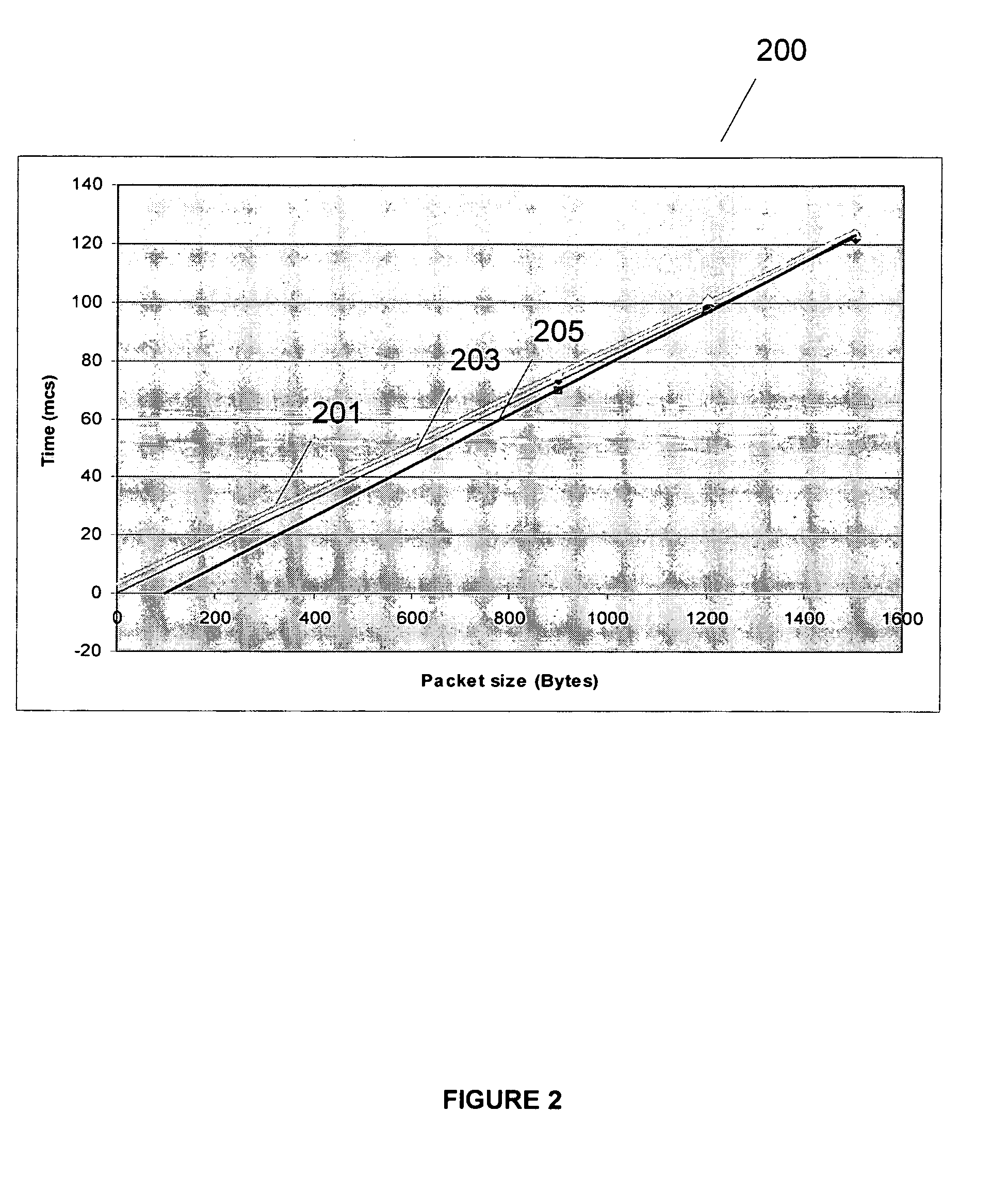
High-accuracy packet pair for network bottleneck bandwidth measurement
PatentInactiveUS7545749B2
Innovation
- A novel packet train transmission technique with filtering and processing of intra and inter packet train delay information is employed to accurately estimate bottleneck bandwidth, using packet trains of varying sizes and additional packets to account for network stability and noise, and employing a history window to ensure stable network conditions.

Chiplet Ecosystem
The Chiplet ecosystem has emerged as a critical component in addressing bandwidth bottlenecks in modern computing systems. This ecosystem encompasses a wide range of technologies, standards, and industry collaborations that enable the development and integration of chiplets into high-performance computing solutions.
At the core of the Chiplet ecosystem are advanced packaging technologies that allow for the integration of multiple silicon dies into a single package. These technologies include 2.5D and 3D packaging, which enable high-bandwidth connections between chiplets and other components. Industry standards such as Universal Chiplet Interconnect Express (UCIe) and Advanced Interface Bus (AIB) have been developed to ensure interoperability and facilitate the adoption of chiplet-based designs across the industry.
The ecosystem also includes a diverse range of chiplet providers, each specializing in specific functionalities such as processing, memory, or I/O. This modular approach allows system designers to mix and match chiplets from different vendors to create customized solutions that meet specific performance and power requirements. Major semiconductor companies, including Intel, AMD, and TSMC, have invested heavily in chiplet technologies and are actively contributing to the ecosystem's growth.
Design and simulation tools play a crucial role in the Chiplet ecosystem, enabling engineers to model and optimize complex multi-die systems. These tools address challenges such as thermal management, signal integrity, and power distribution across chiplet-based designs. Additionally, specialized testing and validation methodologies have been developed to ensure the reliability and performance of chiplet-based systems.
The Chiplet ecosystem has also fostered collaboration between industry players, research institutions, and standardization bodies. Consortiums such as the Open Compute Project (OCP) and CHIPS Alliance are working to develop open standards and reference designs for chiplet-based systems. These collaborative efforts are essential for driving innovation and reducing barriers to entry for new players in the ecosystem.
As the demand for high-bandwidth computing continues to grow, the Chiplet ecosystem is expected to evolve rapidly. Future developments may include more advanced interconnect technologies, improved thermal management solutions, and enhanced design methodologies for heterogeneous integration. The ecosystem's success will be crucial in enabling the next generation of high-performance computing systems across various domains, including data centers, artificial intelligence, and edge computing.
Thermal Management
Thermal management is a critical aspect of chiplet solutions for overcoming bandwidth bottlenecks. As chiplets are integrated more densely to enhance performance and reduce communication latency, the heat generated by these compact components becomes a significant challenge. The increased power density in chiplet-based designs can lead to localized hotspots and overall temperature rise, potentially impacting system reliability and performance.
To address these thermal challenges, various innovative cooling techniques have been developed specifically for chiplet architectures. One approach involves the use of advanced thermal interface materials (TIMs) between chiplets and heat spreaders. These materials, such as indium-based alloys or phase-change materials, offer superior thermal conductivity and help efficiently dissipate heat from the chiplets to the cooling system.
Another strategy focuses on the integration of microfluidic cooling channels directly into the interposer or package substrate. This allows for targeted cooling of high-heat-flux areas, ensuring more uniform temperature distribution across the chiplet array. Some designs incorporate two-phase cooling systems, utilizing the latent heat of vaporization to achieve higher heat transfer rates compared to traditional single-phase liquid cooling.
Advanced packaging technologies also play a crucial role in thermal management for chiplet solutions. 3D packaging techniques, such as through-silicon vias (TSVs) and silicon interposers, can be leveraged not only for electrical connections but also as thermal conduits. These vertical interconnects can help distribute heat more evenly throughout the package, reducing thermal resistance and mitigating hotspots.
Active cooling solutions, such as thermoelectric coolers (TECs) or micro-pumped liquid cooling systems, are being explored for chiplet-based designs with particularly high thermal loads. These active cooling methods can provide precise temperature control and rapid heat removal, albeit at the cost of increased system complexity and power consumption.
Thermal modeling and simulation tools have become indispensable in the design process of chiplet-based systems. Advanced computational fluid dynamics (CFD) simulations and multi-physics modeling enable designers to predict thermal behavior accurately and optimize cooling solutions before physical prototyping. These tools help in identifying potential thermal issues early in the design cycle and guide the placement of chiplets and cooling elements for optimal thermal performance.
As chiplet solutions continue to evolve, thermal management remains a key area of research and development. Future advancements may include the integration of novel materials with high thermal conductivity, such as graphene or carbon nanotubes, into chiplet packages. Additionally, the development of AI-driven thermal management systems that can dynamically adjust cooling parameters based on real-time temperature and workload data holds promise for further improving the thermal efficiency of chiplet-based architectures.
Unlock deeper insights with PatSnap Eureka Quick Research — get a full tech report to explore trends and direct your research. Try now!
Generate Your Research Report Instantly with AI Agent
Supercharge your innovation with PatSnap Eureka AI Agent Platform!