

Comparing Neuromorphic Chips: Reliability vs Cost
SEP 8, 20259 MIN READ
Generate Your Research Report Instantly with AI Agent
Patsnap Eureka helps you evaluate technical feasibility & market potential.
Neuromorphic Computing Evolution and Objectives
Neuromorphic computing represents a paradigm shift in computational architecture, drawing inspiration from the human brain's neural networks to create more efficient and adaptive computing systems. The evolution of this field began in the late 1980s with Carver Mead's pioneering work at Caltech, where he first coined the term "neuromorphic" to describe electronic systems that mimic neuro-biological architectures. This marked the beginning of a journey to develop computing systems that could process information in ways similar to biological neural networks.
The 1990s saw early experimental implementations, primarily focused on analog VLSI circuits that could simulate neural functions. These early systems demonstrated the potential for energy efficiency but were limited in scale and practical application. The 2000s brought significant advancements with the development of digital neuromorphic systems, including IBM's TrueNorth and the SpiNNaker project, which began to address scalability challenges while maintaining the core principles of brain-inspired computing.
The current decade has witnessed an acceleration in neuromorphic chip development, driven by the limitations of traditional von Neumann architectures in handling AI workloads and the increasing demand for edge computing solutions. Major technology companies and research institutions have invested heavily in this area, resulting in chips like Intel's Loihi, BrainChip's Akida, and IBM's second-generation TrueNorth systems.
The primary objectives of neuromorphic computing research center around achieving greater energy efficiency, reducing latency for real-time applications, and enabling adaptive learning capabilities. Unlike traditional computing architectures that separate memory and processing units, neuromorphic designs integrate these functions, potentially reducing the energy consumption by orders of magnitude for certain applications. This is particularly crucial for edge devices with limited power resources.
Another key objective is to develop systems capable of unsupervised and continuous learning, similar to biological neural networks. This would enable devices to adapt to new information without explicit programming, opening possibilities for applications in dynamic environments where conditions frequently change.
In the context of reliability versus cost considerations, neuromorphic computing aims to achieve a balance between system robustness and economic viability. Early neuromorphic chips prioritized experimental capabilities over reliability, but as the field matures, there is increasing focus on developing chips that can maintain consistent performance under varying conditions while remaining cost-effective for commercial applications.
The evolution trajectory suggests that neuromorphic computing is moving from research curiosity to practical implementation, with objectives increasingly aligned with market needs rather than purely academic interests. The ultimate goal remains creating computing systems that combine the adaptability and efficiency of biological brains with the precision and reliability of digital systems.
Market Analysis for Brain-Inspired Computing Solutions
The brain-inspired computing market is experiencing significant growth, driven by the increasing demand for efficient processing of complex AI workloads. Current market valuations place neuromorphic computing at approximately $2.5 billion globally, with projections indicating a compound annual growth rate of 20-25% over the next five years. This growth trajectory is supported by substantial investments from both private and public sectors, with government initiatives in the US, EU, and China allocating dedicated funding for neuromorphic research and development.
Market segmentation reveals diverse application domains for neuromorphic chips, with edge computing, autonomous systems, and scientific research emerging as primary adoption sectors. Edge computing applications represent nearly 40% of the current market share, as neuromorphic solutions offer significant advantages in power efficiency and real-time processing capabilities. The autonomous systems segment, including robotics and self-driving vehicles, constitutes roughly 30% of market demand, valuing reliability over cost considerations due to safety-critical operations.
Customer requirements analysis indicates a clear dichotomy in market preferences. Enterprise customers prioritize reliability metrics, including mean time between failures (MTBF), fault tolerance capabilities, and long-term stability under varying environmental conditions. These customers demonstrate willingness to pay premium prices for chips with proven reliability records, particularly in mission-critical applications. Conversely, research institutions and startups show greater price sensitivity, often accepting lower reliability thresholds to access neuromorphic capabilities within constrained budgets.
The cost structure of neuromorphic chips reveals interesting market dynamics. Production costs remain relatively high compared to traditional computing architectures, primarily due to specialized manufacturing processes and lower production volumes. Current market pricing ranges from $500 for entry-level research-oriented chips to over $10,000 for industrial-grade solutions with comprehensive reliability guarantees. This wide pricing spectrum has created distinct market tiers, with different reliability-cost ratios appealing to different customer segments.
Regional market analysis shows North America leading with approximately 45% market share, followed by Europe (25%) and Asia-Pacific (20%). However, the Asia-Pacific region demonstrates the fastest growth rate, driven by substantial investments in China and emerging neuromorphic ecosystems in Japan and South Korea. These regional differences also reflect varying priorities in the reliability-cost balance, with European markets generally placing higher premiums on reliability metrics compared to more cost-sensitive Asian markets.
Current Challenges in Neuromorphic Chip Development
Despite significant advancements in neuromorphic computing, the field faces several critical challenges that impede widespread adoption and commercialization. One of the primary obstacles is the reliability-cost tradeoff that manufacturers and researchers must navigate. Current neuromorphic chips exhibit inconsistent performance across different operational environments, with temperature fluctuations and electromagnetic interference significantly affecting their computational accuracy and energy efficiency.
Manufacturing scalability presents another substantial hurdle. The complex architecture of neuromorphic systems, which mimic biological neural networks, requires specialized fabrication processes that are difficult to integrate into standard semiconductor production lines. This manufacturing complexity directly impacts production yields and increases per-unit costs, making mass-market adoption economically challenging.
Power consumption optimization remains an unresolved challenge despite the inherent energy efficiency of neuromorphic designs. While these chips theoretically offer significant power advantages over traditional von Neumann architectures, practical implementations often fail to realize these benefits fully. The dynamic power management required for varying computational loads introduces additional complexity that current designs struggle to address efficiently.
Standardization issues further complicate development efforts. The neuromorphic computing field lacks unified benchmarks, programming models, and hardware interfaces. This fragmentation creates significant barriers for software developers and system integrators, limiting the ecosystem growth necessary for sustainable technology advancement. Different research groups and companies employ vastly different approaches to neural encoding, learning algorithms, and hardware-software interfaces.
Memory integration represents a particularly challenging technical barrier. The ideal neuromorphic system requires memory elements that can simultaneously store information and perform computations, similar to biological synapses. Current materials and fabrication techniques for memristive devices and other novel memory technologies still face reliability and endurance limitations that restrict their practical application in commercial neuromorphic systems.
Testing and validation methodologies for neuromorphic chips remain underdeveloped compared to conventional computing systems. The stochastic nature of many neuromorphic computing approaches makes deterministic testing difficult, while the lack of standardized performance metrics complicates comparative analysis between different architectural approaches.
Addressing these challenges requires interdisciplinary collaboration between material scientists, electrical engineers, computer architects, and neuroscientists. Recent research has begun exploring novel materials and 3D integration techniques to improve reliability while reducing manufacturing costs, but significant breakthroughs are still needed before neuromorphic computing can achieve its full potential in commercial applications.
Comparative Analysis of Existing Neuromorphic Architectures
01 Reliability enhancement techniques for neuromorphic chips
Various techniques are employed to enhance the reliability of neuromorphic chips, including fault tolerance mechanisms, redundancy designs, and error correction methods. These approaches help mitigate issues related to device variability, aging effects, and environmental factors that can affect the performance of neuromorphic systems. Advanced testing methodologies are also implemented to ensure consistent operation under different conditions, thereby improving the overall reliability of these chips for critical applications.- Reliability enhancement techniques for neuromorphic chips: Various techniques can be implemented to enhance the reliability of neuromorphic chips, including fault tolerance mechanisms, redundancy systems, and error correction methods. These approaches help mitigate issues related to device variability, aging effects, and environmental factors that can affect the performance of neuromorphic hardware. Advanced testing methodologies and reliability models specific to neuromorphic architectures ensure consistent operation under various conditions, extending the operational lifespan of these specialized chips.
- Cost optimization strategies for neuromorphic computing: Cost optimization for neuromorphic chips involves innovative manufacturing processes, material selection, and architectural designs that reduce production expenses while maintaining performance. Integration of neuromorphic elements with conventional CMOS technology leverages existing fabrication infrastructure, lowering initial investment costs. Scalable designs that allow for efficient mass production and modular approaches enable cost-effective deployment across different application scales, making neuromorphic computing more accessible for commercial applications.
- Energy efficiency and power consumption optimization: Neuromorphic chips are designed to optimize energy efficiency through event-driven processing and spike-based computation, significantly reducing power consumption compared to traditional computing architectures. Advanced power management techniques, including dynamic voltage scaling and selective activation of neural components, further enhance energy efficiency. These optimizations not only reduce operational costs but also address thermal management challenges, enabling more reliable operation in various deployment scenarios while extending battery life in portable applications.
- Fault tolerance and resilience mechanisms: Neuromorphic chips incorporate fault tolerance mechanisms inspired by biological neural systems, allowing them to maintain functionality despite component failures. These include adaptive learning algorithms that can reconfigure neural pathways around damaged areas, graceful degradation capabilities, and built-in self-testing features. Distributed processing architectures inherently provide resilience against localized failures, while specialized hardware monitors can detect and mitigate potential reliability issues before they affect system performance, ensuring consistent operation in critical applications.
- Manufacturing and scaling challenges: The production of neuromorphic chips faces unique manufacturing challenges related to integrating novel materials and maintaining consistency across large-scale neural arrays. Advanced fabrication techniques address issues such as device variability and yield optimization, which directly impact both reliability and cost. Scaling neuromorphic architectures requires balancing increased neural density with interconnect complexity and thermal constraints. Innovative packaging solutions and 3D integration approaches help overcome physical limitations while improving performance-to-cost ratios for commercial viability.
02 Cost optimization strategies in neuromorphic chip manufacturing
Cost optimization in neuromorphic chip manufacturing involves innovative fabrication processes, material selection, and design methodologies that reduce production expenses while maintaining performance standards. Integration of neuromorphic elements with conventional CMOS technology helps leverage existing manufacturing infrastructure, thereby lowering initial investment costs. Additionally, scalable architectures and modular designs enable cost-effective production and easier upgrades, making neuromorphic computing more accessible for commercial applications.Expand Specific Solutions03 Energy efficiency improvements in neuromorphic computing
Neuromorphic chips are designed to mimic the brain's energy-efficient information processing capabilities, significantly reducing power consumption compared to traditional computing architectures. Low-power operation is achieved through event-driven processing, where computations occur only when necessary, and through specialized memory-processing integration that minimizes data movement. These energy efficiency improvements address both cost concerns by reducing operational expenses and reliability issues by decreasing heat generation and associated degradation mechanisms.Expand Specific Solutions04 Novel materials and structures for improved neuromorphic performance
Research into novel materials and structural designs for neuromorphic chips focuses on enhancing both reliability and cost-effectiveness. Memristive devices, phase-change materials, and specialized synaptic elements enable more efficient neural network implementations while potentially reducing manufacturing complexity. Three-dimensional integration techniques increase density and connectivity while maintaining reasonable fabrication costs. These innovations contribute to more robust neuromorphic systems with improved fault tolerance and longer operational lifespans.Expand Specific Solutions05 Testing and validation frameworks for neuromorphic systems
Comprehensive testing and validation frameworks are essential for ensuring neuromorphic chip reliability while controlling development costs. These frameworks include simulation environments, hardware-in-the-loop testing, and specialized benchmarking tools designed specifically for neuromorphic architectures. Accelerated aging tests and environmental stress screening help identify potential failure modes early in the development cycle. By implementing robust validation methodologies, manufacturers can improve yield rates and reduce long-term maintenance costs while ensuring consistent performance in deployed systems.Expand Specific Solutions
Leading Companies and Research Institutions in Neuromorphic Computing
The neuromorphic chip market is currently in a growth phase, characterized by increasing adoption across edge computing applications. The market size is expanding rapidly, driven by demand for energy-efficient AI processing in battery-powered devices. Regarding technical maturity, the field shows varied development levels with established players like IBM, Samsung, and Qualcomm investing heavily in research while newer entrants like Syntiant and Polyn Technology focus on specialized ultra-low-power solutions. Companies are navigating a clear reliability-cost tradeoff, with IBM and Samsung pursuing high-reliability architectures for data centers, while Syntiant and Polyn target cost-effective implementations for edge devices. Academic institutions like KAIST and Tsinghua University are contributing fundamental research to address this balance between performance reliability and manufacturing costs.
International Business Machines Corp.
Technical Solution: IBM's TrueNorth neuromorphic chip represents one of the most advanced implementations in the field, featuring a million programmable neurons and 256 million synapses arranged in 4,096 neurosynaptic cores. The architecture employs a non-von Neumann approach with co-located memory and processing, enabling extremely low power consumption of approximately 70mW during real-time operation[1]. IBM has focused on reliability through redundant neural pathways and fault-tolerant design principles borrowed from biological systems. Their SyNAPSE program has demonstrated that these chips can maintain functionality even when portions of the neural network are damaged or disabled[2]. Cost considerations have been addressed through their 28nm manufacturing process, though production volumes remain relatively limited, keeping per-unit costs higher than conventional processors. IBM has also developed programming frameworks like Corelet to simplify application development for neuromorphic systems[3].
Strengths: Exceptional energy efficiency (20mW per cm²), high fault tolerance through redundant neural pathways, and mature programming tools. Weaknesses: Higher manufacturing costs due to specialized architecture and limited production volumes, complexity in programming compared to traditional computing paradigms, and challenges in scaling to mass production.
Samsung Electronics Co., Ltd.
Technical Solution: Samsung has developed neuromorphic processing units (NPUs) that integrate with their memory technologies, particularly leveraging their expertise in High Bandwidth Memory (HBM) solutions. Their approach focuses on creating neuromorphic systems that combine processing-in-memory (PIM) architectures with specialized neural network accelerators. Samsung's neuromorphic chips utilize their advanced semiconductor manufacturing processes (5nm and below) to create highly integrated solutions that minimize signal travel distance between memory and processing elements[1]. Their reliability strategy emphasizes hardware redundancy and error-correction techniques borrowed from their memory business. Samsung has invested in neuromorphic research through partnerships with academic institutions, focusing on applications in edge computing and IoT devices. Their cost optimization leverages existing manufacturing infrastructure and economies of scale from their memory business, allowing them to potentially produce neuromorphic chips at competitive price points[2]. Recent developments include neuromorphic vision sensors that mimic the human retina for ultra-efficient image processing.
Strengths: Leverages Samsung's advanced semiconductor manufacturing capabilities and memory expertise, potential for cost advantages through existing production infrastructure, and strong integration with mobile and IoT ecosystems. Weaknesses: Less specialized in neuromorphic architecture compared to pure-play neuromorphic companies, still developing programming frameworks and tools for their neuromorphic solutions.
Key Patents and Research Breakthroughs in Neuromorphic Design
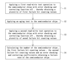
Method for evaluating failure rate
PatentActiveUS20120166130A1
Innovation
- A method involving a first read-write test with error checking and correcting functions turned off, followed by an aging test and a second read-write test, with calculations using failure bit counting values and an error checking and correcting coefficient to determine the failure rate, allowing for a more efficient evaluation process.


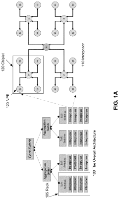
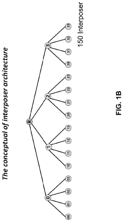
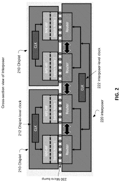
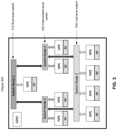
Chiplet-based hierarchical tree topology architecture for neuromorphic computing
PatentPendingUS20240013025A1
Innovation
- A chiplet-based hierarchical tree topology architecture is introduced, where multiple neuron processing entities (NPEs) are organized in a tree topology within chiplets and interposers, with micro-bumps for interconnectivity, and configurable clocks for coordination, enabling efficient short-distance data communication and scalable performance by packaging smaller chiplets into interposers.
Manufacturing Process Impact on Neuromorphic Chip Performance
The manufacturing process of neuromorphic chips significantly influences both their reliability and cost profiles. Traditional CMOS fabrication techniques, while well-established, present challenges when adapted for neuromorphic architectures that mimic biological neural networks. The 7nm and 5nm processes currently employed by industry leaders like Intel and IBM offer increased transistor density but introduce reliability concerns due to quantum tunneling effects and increased susceptibility to manufacturing variations.
Advanced packaging technologies play a crucial role in neuromorphic chip performance. 3D stacking and through-silicon vias (TSVs) enable higher interconnect density between artificial neurons, improving signal integrity while simultaneously increasing manufacturing complexity and yield challenges. These factors directly impact both reliability metrics and production costs, creating a delicate balance that manufacturers must navigate.
Material selection represents another critical manufacturing consideration. While conventional silicon remains dominant, emerging materials like silicon-germanium alloys and III-V semiconductors offer potential performance advantages for neuromorphic applications. However, these alternative materials typically increase manufacturing costs by 30-45% while introducing new reliability variables that require extensive validation.
Defect density management during fabrication directly correlates with neuromorphic chip reliability. Current industry standards target defect densities below 0.1 defects/cm², but neuromorphic architectures with their highly parallel structures demonstrate unique fault tolerance characteristics. Research indicates that certain neuromorphic designs can maintain acceptable performance even with defect rates up to 0.3 defects/cm², potentially allowing for cost optimization through relaxed manufacturing parameters.
Process variation control represents perhaps the most significant manufacturing challenge affecting neuromorphic reliability. Variations in transistor threshold voltages and interconnect resistances can disrupt the carefully calibrated weights in artificial neural networks. Advanced process control techniques, including optical proximity correction and computational lithography, add approximately 15-20% to manufacturing costs but significantly improve chip-to-chip consistency.
Testing methodologies for neuromorphic chips require specialized approaches that differ from conventional digital logic testing. Functional verification must account for the probabilistic nature of neuromorphic computation, necessitating statistical characterization rather than binary pass/fail criteria. This expanded testing regime increases manufacturing costs but ensures reliability metrics accurately reflect real-world performance in machine learning and pattern recognition applications.
Energy Efficiency Considerations in Neuromorphic Computing
Energy efficiency has emerged as a critical factor in the evaluation and implementation of neuromorphic computing systems. Traditional von Neumann architectures consume significant power due to the constant shuttling of data between memory and processing units. In contrast, neuromorphic chips mimic the brain's architecture, where memory and computation are co-located, potentially offering orders of magnitude improvement in energy efficiency.
When comparing neuromorphic chips like IBM's TrueNorth, Intel's Loihi, and BrainChip's Akida, energy consumption metrics reveal substantial differences. TrueNorth operates at approximately 70 milliwatts while running complex neural networks, representing a fraction of the energy required by conventional processors performing similar tasks. Intel's Loihi demonstrates even more impressive efficiency, consuming only 10-30 milliwatts during operation, with energy scaling proportionally to neural activity rather than clock frequency.
The energy advantage of neuromorphic systems stems primarily from their event-driven processing paradigm. Unlike traditional systems that continuously consume power regardless of computational load, neuromorphic chips activate circuits only when necessary—when neurons "fire." This approach mirrors biological neural networks, where energy expenditure correlates directly with information processing requirements.
Material selection also significantly impacts energy profiles. Chips utilizing resistive RAM (ReRAM) or phase-change memory (PCM) as synaptic elements demonstrate lower power requirements compared to SRAM-based implementations. However, these advanced materials often introduce reliability challenges and increased manufacturing costs, creating a complex trade-off landscape.
Thermal management represents another crucial consideration in the energy efficiency equation. Lower power consumption reduces cooling requirements, potentially enabling more compact deployment scenarios and further reducing total system energy costs. This advantage becomes particularly significant in edge computing applications, where power availability may be constrained.
Looking forward, the energy efficiency of neuromorphic systems will likely improve through advancements in materials science, circuit design optimization, and novel architectural approaches. Research into sub-threshold operation and approximate computing techniques shows particular promise for further reducing energy requirements while maintaining acceptable reliability levels.
For practical deployment considerations, organizations must evaluate the total energy cost over the system lifecycle, including not only operational power but also embodied energy from manufacturing processes. The optimal balance between reliability and cost often depends on specific application requirements, with mission-critical systems justifying higher initial investments for improved long-term energy efficiency and reliability.
Unlock deeper insights with Patsnap Eureka Quick Research — get a full tech report to explore trends and direct your research. Try now!
Generate Your Research Report Instantly with AI Agent
Supercharge your innovation with Patsnap Eureka AI Agent Platform!