

Comparing OLED Backplane Technologies for Display Applications
SEP 12, 20259 MIN READ
Generate Your Research Report Instantly with AI Agent
Patsnap Eureka helps you evaluate technical feasibility & market potential.
OLED Backplane Evolution and Objectives
The evolution of OLED (Organic Light-Emitting Diode) backplane technology represents one of the most significant advancements in display technology over the past two decades. Beginning with simple passive matrix designs in the early 2000s, OLED backplanes have undergone substantial transformation to meet increasingly demanding requirements for resolution, power efficiency, and form factor flexibility.
The initial OLED displays utilized amorphous silicon (a-Si) backplanes, borrowed from LCD technology. However, these early implementations suffered from significant limitations in electron mobility, which restricted their application to smaller displays with lower resolution. The technological trajectory shifted dramatically with the introduction of Low-Temperature Polycrystalline Silicon (LTPS) backplanes around 2007, which offered 10-100 times higher electron mobility compared to a-Si.
A pivotal moment in OLED backplane evolution came with the development of oxide semiconductor technologies, particularly Indium Gallium Zinc Oxide (IGZO) in the early 2010s. This technology bridged the gap between a-Si's manufacturing simplicity and LTPS's superior performance characteristics, enabling larger OLED panels with improved uniformity and reduced power consumption.
The most recent technological milestone has been the emergence of flexible and foldable displays, made possible through advanced thin-film transistor (TFT) backplanes on polymer substrates. These developments have fundamentally altered the design possibilities for consumer electronics, allowing for curved, bendable, and even rollable display configurations that were previously impossible with rigid backplane technologies.
Current research objectives in OLED backplane technology are multifaceted, focusing on several critical areas. Primary among these is the enhancement of TFT stability under prolonged operational conditions, particularly addressing threshold voltage shifts that lead to display non-uniformity over time. Another key objective is increasing electron mobility while maintaining manufacturing scalability, which remains essential for cost-effective production of large-format displays.
Additionally, significant research efforts are directed toward reducing power consumption through more efficient backplane designs, as energy efficiency continues to be a crucial factor in portable device applications. The development of backplane technologies compatible with next-generation printing processes represents another important objective, potentially enabling roll-to-roll manufacturing for dramatic cost reductions.
Looking forward, the industry aims to achieve backplane technologies that can support ultra-high resolution (>1000 PPI) displays while maintaining perfect uniformity across increasingly larger panel sizes. The ultimate goal remains the development of backplane solutions that combine optimal performance characteristics with cost-effective manufacturing processes, enabling OLED technology to expand into new application domains beyond current consumer electronics.
Market Analysis for OLED Display Technologies
The OLED display market has experienced remarkable growth over the past decade, evolving from a niche technology to a mainstream display solution across multiple device categories. The global OLED display market reached approximately $38.4 billion in 2021 and is projected to grow at a CAGR of 14.7% through 2028, potentially exceeding $90 billion by that time. This growth trajectory is primarily driven by increasing adoption in smartphones, televisions, and emerging applications in automotive displays and wearable devices.
Smartphones remain the dominant application segment, accounting for over 60% of OLED panel shipments. This dominance stems from OLED's advantages in producing thinner, lighter devices with superior color reproduction and perfect black levels. Apple's adoption of OLED technology for its iPhone lineup since 2017 has significantly accelerated market expansion, while Samsung maintains leadership as both a manufacturer and implementer of OLED displays in its devices.
The television segment represents the fastest-growing market for OLED technology, with annual growth rates exceeding 70% in recent years. LG Display dominates this segment with its WOLED (White OLED) technology, though Samsung's QD-OLED (Quantum Dot OLED) has recently entered the market, introducing new competitive dynamics. Premium pricing remains a barrier to mass adoption, with OLED TVs typically commanding 30-50% price premiums over comparable LCD models.
Regional analysis reveals Asia-Pacific as the manufacturing hub, with South Korea and China accounting for over 85% of global OLED production capacity. However, consumption patterns show more geographic diversity, with North America and Europe representing significant markets for high-end OLED applications. China is rapidly emerging as both a major producer and consumer, with companies like BOE and CSOT expanding their manufacturing capabilities.
The backplane technology landscape shows interesting market segmentation. LTPS (Low-Temperature Polysilicon) dominates the smartphone display segment with approximately 70% market share, while a-Si (amorphous silicon) maintains relevance in cost-sensitive applications. IGZO (Indium Gallium Zinc Oxide) is gaining traction in larger displays and high-resolution applications, with market share growing at 25% annually. Emerging oxide TFT technologies are expected to capture 15% of the market by 2025.
Consumer demand increasingly prioritizes energy efficiency, with manufacturers responding by developing more power-efficient backplane technologies. This trend aligns with broader sustainability initiatives and regulatory requirements for reduced energy consumption in electronic devices. Additionally, flexible and foldable displays represent the fastest-growing premium segment, with annual growth exceeding 50%, driving innovation in backplane technologies that can withstand repeated bending cycles.
Current Backplane Technologies and Limitations
The OLED display industry currently employs several backplane technologies, each with distinct characteristics and limitations. Amorphous Silicon (a-Si) TFT technology, widely used in LCD displays, represents the most mature and cost-effective option. However, a-Si suffers from relatively low electron mobility (typically 0.5-1 cm²/Vs), which limits switching speeds and current-driving capabilities essential for high-resolution OLED displays. Additionally, a-Si exhibits threshold voltage instability under prolonged current stress, leading to brightness inconsistencies across the display over time.
Low-Temperature Polysilicon (LTPS) technology offers significantly higher electron mobility (50-100 cm²/Vs) compared to a-Si, enabling smaller transistors and higher pixel densities. This makes LTPS particularly suitable for high-resolution mobile displays. However, LTPS manufacturing involves complex laser annealing processes that increase production costs and limit scalability to larger display sizes. The non-uniform crystallization process also creates challenges in maintaining consistent performance across large panels.
Indium Gallium Zinc Oxide (IGZO) represents a middle-ground solution with moderate electron mobility (10-20 cm²/Vs) and better uniformity than LTPS. IGZO offers improved stability under electrical stress compared to a-Si while maintaining reasonable manufacturing costs. However, IGZO remains sensitive to environmental factors such as humidity and light exposure, which can affect long-term reliability and necessitate additional encapsulation measures.
Oxide TFT technologies beyond IGZO, including zinc tin oxide (ZTO) and indium zinc oxide (IZO), show promise but face challenges in process stability and material optimization. These emerging technologies require further development to achieve consistent performance in mass production environments.
Organic TFTs present an alternative approach with potential for flexible displays but currently suffer from low mobility (typically <1 cm²/Vs) and stability issues. While offering advantages in flexibility and potentially lower processing temperatures, organic semiconductors remain vulnerable to degradation from oxygen and moisture exposure.
Each backplane technology faces common challenges in scaling to larger display sizes while maintaining uniform electrical characteristics. As OLED displays push toward higher resolutions, refresh rates, and brightness levels, current backplane technologies struggle to deliver sufficient current density without compromising lifetime or increasing power consumption. The industry also faces significant yield challenges when implementing advanced backplane technologies, particularly for large-area displays where defect rates directly impact manufacturing costs.
Comparative Analysis of TFT Backplane Solutions
01 Thin-Film Transistor (TFT) Technologies for OLED Backplanes
Various thin-film transistor technologies are employed in OLED backplanes to drive the display pixels. These include low-temperature polysilicon (LTPS), oxide semiconductors like IGZO, and organic TFTs. These technologies offer different performance characteristics in terms of electron mobility, stability, and manufacturing complexity, affecting the overall display performance and power efficiency.- Thin-Film Transistor (TFT) Technologies for OLED Backplanes: Various thin-film transistor technologies are employed in OLED backplanes to drive the display pixels. These include low-temperature polysilicon (LTPS), amorphous silicon (a-Si), and oxide semiconductor technologies like indium gallium zinc oxide (IGZO). These TFT technologies offer different performance characteristics in terms of electron mobility, stability, and manufacturing complexity, affecting the overall display performance and production cost.
- Flexible and Foldable OLED Backplane Structures: Innovations in flexible and foldable OLED backplane technologies enable bendable display applications. These technologies incorporate specialized substrate materials, encapsulation methods, and structural designs that maintain electrical performance while allowing physical deformation. Flexible backplanes typically use plastic substrates and specialized thin-film deposition techniques to achieve the required mechanical properties while maintaining display functionality.
- Circuit Design and Pixel Driving Schemes: Advanced circuit designs and pixel driving schemes are critical for OLED backplane performance. These include compensation circuits to address TFT threshold voltage variations, current programming methods to ensure uniform brightness, and various pixel circuit architectures to improve display quality. These driving schemes help overcome issues like non-uniformity, image sticking, and power consumption in OLED displays.
- Integration Technologies and Manufacturing Methods: Specialized integration technologies and manufacturing methods are employed for OLED backplane production. These include advanced photolithography processes, etching techniques, and deposition methods that enable high-resolution displays with improved yield rates. Integration approaches also address challenges in connecting the backplane with the OLED front plane and peripheral driving circuits to create complete display modules.
- Novel Materials and Structures for Enhanced Performance: Novel materials and structural innovations are being developed to enhance OLED backplane performance. These include new semiconductor materials with improved electron mobility, innovative electrode structures for better charge injection, and advanced passivation layers to protect against environmental degradation. These materials and structures aim to improve display brightness, efficiency, lifetime, and resolution while potentially reducing manufacturing costs.
02 Flexible and Foldable OLED Backplane Structures
Innovations in flexible and foldable OLED backplane structures enable bendable display applications. These technologies incorporate specialized substrate materials, encapsulation techniques, and stress-resistant circuit designs to maintain electrical performance during bending. The flexible backplanes often utilize thin-film technologies on plastic or ultra-thin glass substrates with specialized buffer layers to manage mechanical stress.Expand Specific Solutions03 Integration and Compensation Circuits in OLED Backplanes
Advanced integration and compensation circuits are incorporated into OLED backplanes to address pixel non-uniformity and aging issues. These circuits include threshold voltage compensation, current programming, and external compensation schemes that improve display uniformity and extend the operational lifetime of OLED displays. The integration of these circuits with driving transistors helps maintain consistent brightness across the display panel.Expand Specific Solutions04 Manufacturing Processes for OLED Backplanes
Specialized manufacturing processes are developed for OLED backplanes, including advanced photolithography, laser annealing, and solution-based deposition methods. These processes aim to improve yield, reduce production costs, and enable high-resolution displays. Innovations in manufacturing include multi-step annealing processes for semiconductor layers and specialized etching techniques that enhance transistor performance and stability.Expand Specific Solutions05 Novel Materials for OLED Backplane Components
Novel materials are being developed for OLED backplane components to enhance performance and enable new functionalities. These include advanced semiconductor materials, transparent conductive oxides, and dielectric materials with improved electrical properties. The use of these materials can lead to higher electron mobility, better optical transparency, and improved stability under operational conditions, resulting in enhanced display performance.Expand Specific Solutions
Leading Manufacturers and Competitive Landscape
The OLED backplane technology market is currently in a growth phase, with an estimated market size exceeding $30 billion and projected to expand significantly as OLED displays gain wider adoption in consumer electronics. The competitive landscape is dominated by Asian manufacturers, particularly Chinese companies like BOE Technology Group, TCL China Star Optoelectronics, and HKC Corp, alongside established players like LG Display. Technologically, the industry is transitioning from traditional amorphous silicon (a-Si) backplanes toward more advanced technologies including Low-Temperature Polycrystalline Silicon (LTPS) and Oxide TFT (IGZO) backplanes. Universal Display Corporation and Novaled GmbH are leading material technology providers, while Apple and Meta represent major end-users driving innovation requirements. The technology is approaching maturity for mobile applications but remains in development for larger display formats.
BOE Technology Group Co., Ltd.
Technical Solution: BOE has developed a comprehensive portfolio of OLED backplane technologies, focusing on both rigid and flexible display applications. Their primary technologies include LTPS (Low-Temperature Polysilicon) for small to medium displays and oxide semiconductor (primarily IGZO) backplanes for larger panels. BOE's advanced LTPS technology achieves electron mobility of approximately 80-100 cm²/Vs, enabling high-resolution, high-refresh-rate displays for premium smartphone applications. For their flexible OLED displays, BOE employs a specialized thin-film encapsulation process combined with optimized LTPS backplanes that can withstand repeated bending while maintaining electrical performance. The company has also pioneered hybrid backplane architectures that combine the benefits of different TFT technologies - using LTPS for driving circuits and oxide TFTs for pixel arrays - to optimize both performance and production costs. Recent innovations include ultra-low temperature polysilicon processes that reduce thermal stress on flexible substrates.
Strengths: Extensive manufacturing capacity across multiple backplane technologies; strong vertical integration from materials to finished displays; advanced flexible OLED capabilities with specialized backplane designs. Weaknesses: Still catching up to Korean manufacturers in high-end OLED production yields; oxide TFT technology faces challenges in achieving the electron mobility needed for the highest performance applications; higher power consumption in some backplane implementations compared to competitors.
TCL China Star Optoelectronics Technology Co., Ltd.
Technical Solution: TCL CSOT has developed proprietary OLED backplane technologies centered around their "LTPO 2.0" (Low-Temperature Polycrystalline Oxide) architecture. This hybrid technology combines elements of LTPS and oxide TFT to achieve variable refresh rates (1-120Hz) while significantly reducing power consumption by up to 20% compared to conventional LTPS backplanes. Their manufacturing process employs a unique multi-layer deposition technique that improves electron mobility (achieving ~40-50 cm²/Vs) while maintaining production efficiency. For large-format displays, TCL has pioneered an advanced oxide semiconductor backplane with specialized compensation circuits that address threshold voltage shifts common in oxide TFTs, resulting in more uniform brightness across the display. Their latest innovation includes a micro-patterned backplane architecture that improves aperture ratio by approximately 15%, enhancing overall luminous efficiency. TCL has also developed specialized backplane solutions for foldable displays that maintain electrical performance at the fold area through a proprietary stress-relief layer structure.
Strengths: Cost-effective manufacturing processes for mid-range OLED displays; innovative LTPO technology with excellent power efficiency; strong capabilities in large-format OLED panels with oxide backplanes. Weaknesses: Lower electron mobility compared to industry leaders' LTPS solutions; production yield challenges for the highest resolution displays; less mature flexible display technology compared to competitors like Samsung and LG.
Key Patents and Innovations in Backplane Design
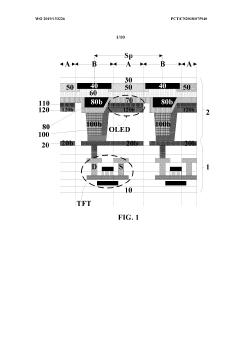
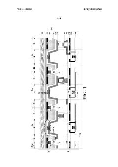
Organic light emitting diode display panel, organic light emitting diode counter substrate, and fabricating method thereof
PatentWO2019153226A1
Innovation
- Inverted OLED structure with organic light emitting diodes located on the counter substrate rather than the array substrate, which enables more efficient driving of the display panel.
- Implementation of a spacer layer in the inter-subpixel region to maintain precise spacing between the array substrate and counter substrate, enhancing structural stability and display uniformity.
- Use of a substantially transparent electrode layer on the spacer layer that connects to the thin film transistors, allowing for efficient electrical connectivity while maintaining optical transparency.
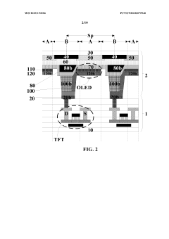
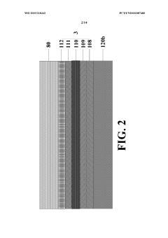
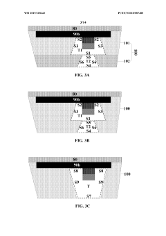
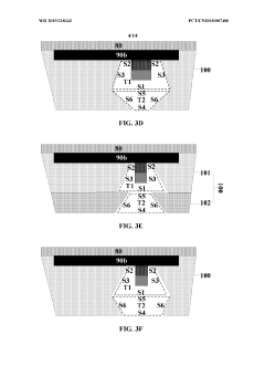
Organic light emitting diode counter substrate and display panel, array substrate for organic light emitting diode display panel, and fabricating method thereof
PatentWO2019218342A1
Innovation
- Separation of OLED components between array and counter substrates, with organic light emitting diodes placed on the counter substrate while driving thin film transistors remain on the array substrate.
- Implementation of a first electrode layer that electrically connects the OLEDs on the counter substrate to the driving TFTs on the array substrate, enabling a novel device architecture.
- Integration of spacer blocks within each subpixel to maintain precise spacing between the array substrate and counter substrate.
Manufacturing Process Optimization Strategies
Optimizing manufacturing processes for OLED backplane technologies represents a critical factor in determining commercial viability and performance characteristics of display products. Current manufacturing optimization strategies focus on several key areas that significantly impact yield rates, cost structures, and final device performance.
Yield improvement techniques have evolved substantially across different backplane technologies. For LTPS (Low-Temperature Polysilicon) backplanes, laser annealing process refinements have reduced defect densities by approximately 30% over the past five years. Implementation of advanced statistical process control systems enables real-time monitoring of critical parameters during crystallization phases, allowing for immediate adjustments that maintain optimal grain structure formation.
Material utilization efficiency presents another crucial optimization vector. Modern IGZO (Indium Gallium Zinc Oxide) manufacturing lines have achieved up to 85% material utilization rates through implementation of precision deposition techniques and recycling systems. Particularly noteworthy is the development of rotary target sputtering technology, which extends target lifetime while maintaining consistent film quality across large substrate areas.
Throughput enhancement strategies differ significantly between backplane technologies. LTPS processes benefit from multi-beam laser systems that can process larger substrate areas simultaneously, while oxide TFT manufacturing has seen improvements through parallel processing architectures. Advanced a-Si (amorphous silicon) lines now implement cluster tool configurations that reduce transfer times between process chambers by up to 40% compared to previous generation equipment.
Energy consumption reduction represents both an economic and environmental imperative. Recent innovations in low-temperature processing for oxide semiconductors have reduced thermal budget requirements by approximately 25% compared to traditional methods. Additionally, vacuum system optimizations have decreased pump-down times and associated energy costs across all backplane technologies.
Defect management systems have become increasingly sophisticated, with AI-powered optical inspection tools capable of detecting and classifying defects with sub-micron precision. These systems are particularly valuable for LTPS backplanes, where grain boundary defects can significantly impact device performance. Integration of these inspection systems with manufacturing execution systems (MES) enables closed-loop process control that continuously refines process parameters.
Equipment utilization metrics have become standardized across the industry, with Overall Equipment Effectiveness (OEE) serving as a key performance indicator. Leading manufacturers now achieve OEE rates exceeding 85% for established processes, though new backplane technologies typically require 12-18 months to reach comparable efficiency levels as process knowledge accumulates.
Environmental Impact and Sustainability Considerations
The environmental footprint of OLED display manufacturing varies significantly depending on the backplane technology employed. LTPS (Low-Temperature Polysilicon) manufacturing processes typically require higher energy consumption due to multiple annealing steps and complex photolithography sequences. These processes generate substantial greenhouse gas emissions and utilize various chemicals that require careful disposal. In contrast, oxide TFT technologies like IGZO (Indium Gallium Zinc Oxide) generally demonstrate lower energy requirements during fabrication, with fewer processing steps and lower temperature requirements, resulting in a reduced carbon footprint.
Material usage represents another critical environmental consideration. LTPS backplanes require larger quantities of rare and precious metals compared to a-Si or oxide TFT alternatives. The extraction and processing of these materials often involve environmentally damaging mining practices and energy-intensive purification processes. IGZO backplanes utilize indium, which faces potential supply constraints, though they generally require less silicon and other semiconductor materials than LTPS counterparts.
End-of-life management presents significant challenges across all OLED backplane technologies. The complex integration of organic materials with inorganic substrates and various metals makes recycling particularly difficult. LTPS displays contain higher concentrations of valuable materials that could theoretically justify more intensive recycling efforts, yet the intricate separation processes required often limit practical recovery rates. Oxide TFT backplanes may offer marginally better recyclability profiles due to their simpler material composition.
Power efficiency during operation represents a sustainability advantage for advanced backplane technologies. LTPS and oxide TFT backplanes enable lower power consumption in finished displays compared to a-Si alternatives, resulting in reduced lifetime energy usage. This operational efficiency can partially offset higher manufacturing impacts, particularly for devices with longer usage lifespans. IGZO backplanes specifically excel in this regard, offering superior power efficiency that translates to extended battery life in portable devices.
Manufacturing waste generation varies considerably between technologies. LTPS fabrication typically produces more hazardous waste streams due to the extensive use of dopants and etchants. The higher temperatures and more complex processes also lead to higher rejection rates during production. Oxide TFT manufacturing generally creates less hazardous waste and demonstrates better yield rates, though all backplane technologies still generate substantial waste requiring specialized treatment and disposal protocols.
Water consumption represents another significant environmental impact, with LTPS manufacturing requiring substantially more ultrapure water for cleaning and processing steps than oxide TFT alternatives. This places additional strain on local water resources in manufacturing regions, many of which already face water scarcity challenges.
Unlock deeper insights with Patsnap Eureka Quick Research — get a full tech report to explore trends and direct your research. Try now!
Generate Your Research Report Instantly with AI Agent
Supercharge your innovation with Patsnap Eureka AI Agent Platform!