How to Measure Current Uniformity Across OLED Arrays
SEP 12, 20259 MIN READ
Generate Your Research Report Instantly with AI Agent
Patsnap Eureka helps you evaluate technical feasibility & market potential.
OLED Current Uniformity Measurement Background and Objectives
Organic Light-Emitting Diode (OLED) technology has revolutionized display and lighting industries since its commercial introduction in the late 1990s. The evolution of OLED technology has been marked by significant improvements in efficiency, lifetime, and manufacturing processes. Current uniformity across OLED arrays represents one of the critical parameters that directly impacts display quality, device longevity, and energy efficiency. This technical investigation aims to comprehensively examine methodologies for measuring and ensuring current uniformity in OLED arrays.
The fundamental principle of OLED operation relies on the injection of electrons and holes from opposite electrodes into an emissive layer, where their recombination produces light. Ideally, this current flow should be uniform across the entire array to ensure consistent brightness and color accuracy. However, manufacturing variations, material inconsistencies, and design limitations often lead to non-uniform current distribution, resulting in visible defects such as mura patterns, brightness variations, and accelerated degradation in specific areas.
Historical approaches to measuring current uniformity have evolved from simple optical inspection methods to sophisticated electrical characterization techniques. Early detection methods primarily focused on identifying visible non-uniformities in finished displays, which proved inadequate for preventive quality control. The industry subsequently developed more proactive measurement techniques, including in-line electrical testing during manufacturing and advanced imaging systems capable of detecting subtle variations in current flow.
The primary objective of this investigation is to evaluate existing methodologies for measuring current uniformity across OLED arrays and identify their respective strengths and limitations. Additionally, we aim to explore emerging technologies and approaches that could potentially enhance measurement accuracy, speed, and cost-effectiveness. The ultimate goal is to establish a comprehensive framework for current uniformity measurement that can be integrated into both research and production environments.
Another critical objective is to correlate current uniformity measurements with actual display performance metrics and device lifetime. This correlation would enable manufacturers to establish meaningful specifications and tolerance limits for current uniformity, thereby optimizing the balance between manufacturing yield and product quality. Furthermore, understanding this relationship could guide the development of compensation algorithms and circuit designs to mitigate the effects of inherent non-uniformities.
This investigation also seeks to address the increasing complexity of current uniformity measurement in next-generation OLED technologies, including flexible displays, transparent OLEDs, and high-resolution micro-displays for augmented reality applications. These emerging applications present unique challenges for current uniformity measurement due to their form factors, operating conditions, and performance requirements.
Market Demand Analysis for Uniform OLED Displays
The global demand for uniform OLED displays has witnessed exponential growth over the past decade, driven primarily by the consumer electronics sector. Market research indicates that the OLED display market reached approximately $48 billion in 2022, with projections suggesting growth to $72 billion by 2026. Within this expanding market, display uniformity has emerged as a critical differentiating factor, with manufacturers competing intensely on quality metrics rather than merely price points.
Consumer expectations regarding display quality have evolved significantly, with end-users demonstrating increasing sensitivity to even minor uniformity issues. Recent consumer studies reveal that over 70% of smartphone users can detect brightness inconsistencies across their screens, with 65% considering this a significant factor in purchasing decisions. This heightened consumer awareness has transformed current uniformity from a technical specification to a market imperative.
The premium device segment demonstrates particularly stringent requirements, with high-end smartphone and television manufacturers implementing increasingly rigorous uniformity standards. Apple's display specifications, for instance, have tightened uniformity tolerances by 30% in their latest generation devices compared to models from five years ago, establishing new industry benchmarks that competitors must match.
Commercial applications represent another significant market driver, with sectors such as medical imaging, automotive displays, and professional monitors demanding exceptional uniformity. The medical display market, valued at $2.2 billion, requires current uniformity variations below 1.5% for diagnostic accuracy, while automotive displays must maintain uniformity across extreme temperature ranges and operating conditions.
Emerging technologies like foldable and transparent displays have introduced additional uniformity challenges, creating new market segments for specialized measurement and calibration solutions. The foldable display market, growing at 35% annually, faces unique uniformity issues at fold points, driving demand for advanced measurement techniques capable of characterizing these complex geometries.
Manufacturing yield improvements represent perhaps the most compelling economic driver for uniformity measurement solutions. Industry data suggests that improving current uniformity detection during production can increase manufacturing yields by 8-12%, translating to millions in cost savings for large-scale producers. This economic incentive has spurred investment in advanced measurement technologies throughout the supply chain.
The geographical distribution of market demand follows OLED manufacturing centers, with East Asia (particularly South Korea, Japan, and China) representing 78% of the global market for uniformity measurement solutions. However, research and development activities show a more distributed pattern, with significant innovation clusters in Europe and North America focusing on next-generation measurement technologies.
Current Challenges in OLED Array Current Distribution
Despite significant advancements in OLED technology, achieving uniform current distribution across OLED arrays remains a persistent challenge that impacts display quality, efficiency, and device longevity. The non-uniform current distribution manifests as brightness variations, color shifts, and accelerated degradation in specific areas of displays, undermining the overall performance of OLED-based products.
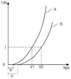
A primary challenge stems from the inherent characteristics of thin-film transistors (TFTs) used in active-matrix OLED displays. These TFTs exhibit threshold voltage variations and mobility inconsistencies due to manufacturing process limitations, resulting in different current levels being delivered to individual OLED pixels even when identical control signals are applied. This variation becomes more pronounced as display sizes increase and pixel densities rise.
The architecture of OLED arrays presents additional complications. Voltage drops along power supply lines create position-dependent current variations, with pixels farther from power sources receiving less current than those positioned closer. This issue intensifies in large-format displays and high-resolution applications where power distribution networks become more complex and extended.
Temperature gradients across display panels further exacerbate current uniformity problems. OLEDs are temperature-sensitive devices whose electrical characteristics change significantly with temperature fluctuations. During operation, different regions of a display may develop varying temperatures due to uneven power dissipation, creating a feedback loop that amplifies current non-uniformity.
Material degradation introduces temporal aspects to the uniformity challenge. OLEDs experience differential aging based on usage patterns, with frequently activated pixels degrading faster than less-used ones. This leads to evolving current distribution patterns over the device lifetime, requiring dynamic compensation strategies rather than static solutions.
Measurement and characterization of these non-uniformities present their own set of challenges. Traditional techniques often provide only aggregate or indirect measurements that fail to capture the spatial and temporal dynamics of current distribution. High-resolution, real-time current mapping across large arrays remains technically difficult and commercially impractical for production environments.
The industry also faces challenges in developing effective compensation algorithms. While various approaches exist for brightness uniformity correction, many address symptoms rather than the underlying current distribution issues. Additionally, these algorithms must balance correction accuracy against computational complexity and power consumption, particularly in mobile applications where resources are constrained.
Existing Current Uniformity Measurement Solutions
01 Compensation circuits for current uniformity
Compensation circuits are implemented in OLED arrays to address current non-uniformity issues caused by threshold voltage variations in driving transistors. These circuits detect and compensate for variations in transistor characteristics, ensuring uniform current flow to each OLED pixel regardless of transistor threshold voltage differences. This approach significantly improves display quality by maintaining consistent brightness across the entire array.- Compensation circuits for current uniformity: Compensation circuits are integrated into OLED arrays to address variations in driving current that lead to non-uniform brightness. These circuits detect and adjust for threshold voltage variations in thin-film transistors (TFTs) and compensate for aging effects in OLED pixels. By implementing feedback mechanisms that monitor actual current flow and make real-time adjustments, these compensation techniques significantly improve current uniformity across the display panel.
- Pixel circuit design for uniform current distribution: Advanced pixel circuit designs incorporate additional transistors and capacitors to ensure uniform current distribution across OLED arrays. These designs minimize the impact of manufacturing variations and electrical stress on current delivery. By implementing voltage programming, current scaling, and charge storage elements within each pixel, these circuits maintain consistent current levels regardless of position within the array or operational duration, resulting in improved visual uniformity.
- Driving methods to improve current uniformity: Specialized driving methods are employed to enhance current uniformity in OLED arrays. These include time-division driving schemes, pulse width modulation techniques, and voltage-programmed current sources. By precisely controlling the timing and amplitude of driving signals, these methods compensate for inherent variations in OLED characteristics. Advanced driving algorithms dynamically adjust parameters based on display content and operational conditions to maintain consistent current delivery across the entire array.
- Sensing and feedback systems for current control: Integrated sensing and feedback systems continuously monitor current flow through OLED pixels and make real-time adjustments to maintain uniformity. These systems incorporate current sensors, analog-to-digital converters, and control logic to detect deviations from target current levels. The feedback mechanisms compensate for manufacturing variations, temperature fluctuations, and aging effects by dynamically adjusting driving parameters, ensuring consistent brightness across the display regardless of external conditions or operational history.
- Material and structural improvements for current uniformity: Material innovations and structural enhancements in OLED arrays significantly improve current uniformity. These include optimized semiconductor materials for TFTs, improved OLED stack designs with uniform charge transport layers, and novel electrode configurations that ensure even current distribution. Advanced manufacturing techniques reduce variations in layer thickness and material properties, while specialized encapsulation methods protect against environmental factors that could lead to non-uniform degradation, collectively resulting in more consistent current flow across the display.
02 Pixel circuit designs for improved current distribution
Advanced pixel circuit designs incorporate additional transistors and capacitors to regulate current flow to OLED elements. These circuits implement voltage sampling, current programming, or digital compensation techniques to ensure uniform current delivery regardless of manufacturing variations. By isolating the OLED from direct dependence on transistor characteristics, these designs achieve more consistent luminance across large display arrays.Expand Specific Solutions03 Driving methods for current uniformity
Specialized driving methods are employed to improve current uniformity in OLED arrays. These include time-division driving schemes, pulse width modulation techniques, and current-programmed driving methods. By precisely controlling the timing and amplitude of driving signals, these methods compensate for variations in transistor characteristics and OLED performance, resulting in more uniform brightness across the display panel.Expand Specific Solutions04 Sensing and feedback systems
Sensing and feedback systems continuously monitor the actual current flowing through OLED pixels and adjust driving parameters in real-time. These systems incorporate current sensors, analog-to-digital converters, and feedback algorithms to detect deviations from desired current levels and apply appropriate corrections. This closed-loop approach ensures consistent current delivery to each pixel despite aging effects and manufacturing variations.Expand Specific Solutions05 Material and structural optimizations
Material selection and structural design optimizations are implemented to enhance current uniformity in OLED arrays. These include improved semiconductor materials for transistors, optimized electrode configurations, and novel device architectures that minimize the impact of process variations. By addressing the fundamental physical causes of current non-uniformity, these approaches provide more consistent performance across large-area displays.Expand Specific Solutions
Leading Companies in OLED Testing Equipment
The OLED current uniformity measurement technology landscape is evolving rapidly, currently in a growth phase with increasing market adoption across display manufacturing. The global market is expanding significantly as OLED displays become mainstream in consumer electronics. Technologically, the field shows varying maturity levels among key players. Industry leaders like Samsung Display and LG Display demonstrate advanced capabilities with established measurement solutions, while BOE Technology and TCL China Star are rapidly advancing their technologies. Companies like IGNIS Innovation offer specialized solutions addressing uniformity challenges. Emerging players such as Tianma Microelectronics and Visionox are developing competitive technologies, creating a dynamic competitive environment where both established manufacturers and specialized solution providers compete for technological leadership in ensuring OLED display quality and performance.
BOE Technology Group Co., Ltd.
Technical Solution: BOE Technology has developed an integrated current uniformity measurement system for OLED arrays that combines on-panel sensing with external verification equipment. Their approach utilizes thin-film current sensors embedded within the display backplane that can measure current flow through individual pixels or pixel groups without significantly impacting display design. The system employs a time-division multiplexing architecture to sequentially measure currents across the entire panel with minimal additional circuitry. BOE's technology features high-precision analog-to-digital converters that can detect current variations as small as 0.2% between adjacent pixels. Their methodology includes both dark current measurements (to establish baseline uniformity) and active measurements under various gray levels to characterize the full operating range. The collected data is processed through proprietary algorithms that generate current distribution maps, highlighting areas of non-uniformity and classifying defects based on spatial patterns. BOE has also implemented automated calibration systems that can adjust driving parameters based on measured current variations to improve final display uniformity.
Strengths: Minimal impact on display design while providing comprehensive measurement capability; scalable approach suitable for various panel sizes; integrated solution that supports both manufacturing quality control and in-field monitoring. Weaknesses: Limited measurement precision compared to dedicated external equipment; additional processing overhead required for data analysis; potential interference from other panel components affecting measurement accuracy.
Samsung Display Co., Ltd.
Technical Solution: Samsung Display has developed advanced current uniformity measurement systems for OLED arrays that combine real-time electrical monitoring with optical inspection. Their approach utilizes a multi-point sensing architecture that measures current distribution across the entire panel during operation. The system employs high-precision current sensors integrated into the OLED backplane to detect variations as small as 0.1% between pixels. Samsung's proprietary algorithm analyzes temporal current patterns to identify aging-related non-uniformities before they become visually apparent. Their technology also incorporates compensation circuits that can adjust driving signals based on measured current variations, creating a closed-loop system that maintains uniformity throughout the display's lifetime. Recent implementations include machine learning models that predict uniformity degradation patterns based on historical measurement data.
Strengths: Highly integrated approach combining hardware sensing with software compensation; exceptional precision in current variation detection; predictive capabilities for panel lifetime management. Weaknesses: Complex implementation requiring specialized manufacturing processes; higher production costs compared to simpler testing methods; system overhead may impact overall power efficiency in mobile applications.
Key Technologies for OLED Array Current Analysis
Display device
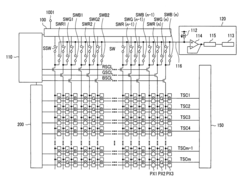
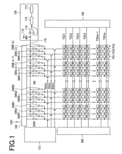
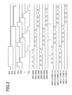
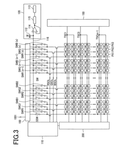
PatentActiveUS20080218499A1
Innovation
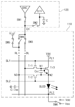
- A display device design that allows simultaneous measurement of voltage-current characteristics of multiple OLED elements by using a matrix arrangement with signal and scanning lines, detection switches, and a constant current source, enabling the detection of groups of pixels at once, including those of the same or different colors, to reduce measurement time and power consumption.
Organic light emitting diode display device and method of measuring capacity of pixel current measuring line of the same
PatentActiveKR1020130107607A
Innovation
- An OLED display device and method that calculates line capacitance and pixel current using voltage variations, employing a compensation coefficient calculator to quickly measure pixel currents and compensate image signals by calculating offset and gain values based on line capacitance and pixel characteristics.
Quality Control Standards for OLED Manufacturing
Quality control standards in OLED manufacturing have evolved significantly to address the critical challenge of current uniformity across arrays. These standards now incorporate sophisticated measurement protocols that combine electrical, optical, and thermal testing methodologies. The International Electrotechnical Commission (IEC) has established benchmark standards such as IEC 62341-6-3, which specifically addresses uniformity requirements for OLED displays, mandating less than 5% variation in current distribution across active matrix arrays.
Leading manufacturers have implemented multi-tiered quality control frameworks that begin with substrate inspection and continue through to final assembly. These frameworks typically require current uniformity measurements at multiple production stages, with increasingly stringent tolerances as the manufacturing process advances. For example, panel-level testing often permits up to 8% variation in current distribution, while module-level quality control standards reduce this allowance to 3-5%.
Statistical Process Control (SPC) methodologies have become integral to OLED manufacturing standards, with control charts specifically designed to monitor current uniformity trends. These systems typically trigger investigation protocols when uniformity variations exceed two standard deviations from established baselines, and implement production halts at three standard deviations.
The Display Measurement Standard (DMS) developed by the Society for Information Display (SID) provides comprehensive guidelines for uniformity assessment, including specific protocols for current distribution measurement across OLED arrays. These standards prescribe measurement conditions, sampling frequencies, and statistical analysis methods to ensure consistency across the industry.
Environmental parameters significantly impact measurement accuracy, leading to standardized testing conditions: 23±2°C temperature, 40-60% relative humidity, and controlled ambient lighting below 5 lux. Quality control standards now mandate that uniformity measurements be conducted under these controlled conditions to ensure reproducibility and comparability of results.
Calibration standards for measurement equipment have also been formalized, requiring traceability to national metrology institutes and regular verification against reference standards. Equipment used for current uniformity measurement typically requires calibration certification renewal every 6-12 months, depending on usage intensity and environmental factors.
Documentation requirements have become increasingly comprehensive, with standards now mandating detailed records of measurement methodologies, equipment specifications, environmental conditions, and statistical analysis procedures. These records must be maintained for a minimum of five years and be available for audit by certification bodies and major customers.
Impact of Current Non-uniformity on Display Performance
Current non-uniformity in OLED arrays significantly impacts display performance across multiple dimensions. The most immediate effect is visible brightness variations across the display panel, resulting in uneven luminance that degrades image quality. Even minor current variations of 5-10% can produce noticeable brightness inconsistencies that compromise the viewing experience, particularly in applications requiring high visual fidelity such as professional image editing or medical diagnostics.
Beyond brightness issues, current non-uniformity causes color accuracy problems. Since different OLED materials (red, green, and blue) may respond differently to current variations, non-uniform current distribution can lead to color shifts across the display. This phenomenon is particularly problematic in applications where color consistency is critical, such as in color-calibrated professional displays or high-end consumer televisions.
Display lifetime and reliability are also severely affected by current non-uniformity. OLED pixels subjected to higher current densities degrade faster than those operating at nominal levels, creating accelerated aging in specific panel regions. This differential aging exacerbates non-uniformity over time, as initially minor variations become more pronounced through the display's operational life.
Power efficiency suffers as well, as non-uniform current distribution typically results in some pixels drawing excess current while others receive insufficient power. This inefficiency increases overall power consumption and heat generation, further accelerating pixel degradation and potentially triggering thermal management issues in compact display designs.
From a manufacturing perspective, current non-uniformity directly impacts production yields. Displays exhibiting excessive non-uniformity may fail quality control standards, increasing production costs and reducing manufacturing efficiency. The economic impact becomes particularly significant in high-volume production environments where even small yield reductions translate to substantial financial losses.
Advanced display technologies such as high dynamic range (HDR) and wide color gamut implementations are especially vulnerable to current non-uniformity effects. These technologies demand precise control over brightness and color reproduction across the entire display surface, making current uniformity a critical factor in achieving the intended visual performance and maintaining competitive advantage in premium display markets.
Unlock deeper insights with Patsnap Eureka Quick Research — get a full tech report to explore trends and direct your research. Try now!
Generate Your Research Report Instantly with AI Agent
Supercharge your innovation with Patsnap Eureka AI Agent Platform!