

Optimize OLED Vapor Deposition Rate for Increased Yields
SEP 12, 20259 MIN READ
Generate Your Research Report Instantly with AI Agent
Patsnap Eureka helps you evaluate technical feasibility & market potential.
OLED Vapor Deposition Technology Background and Objectives
Organic Light-Emitting Diode (OLED) technology has revolutionized display and lighting industries since its commercial introduction in the late 1990s. The vapor deposition process, particularly in manufacturing OLED panels, represents a critical production step that directly impacts product quality, manufacturing efficiency, and ultimately, market competitiveness. This technology evolved from basic vacuum thermal evaporation methods to sophisticated organic vapor phase deposition (OVPD) and low-temperature polycrystalline silicon (LTPS) processes currently employed in high-end manufacturing facilities.
The historical trajectory of OLED vapor deposition technology shows significant advancements in precision, uniformity, and throughput. Early implementations suffered from inconsistent layer formation, material wastage exceeding 70%, and limited scalability. Modern systems have dramatically improved these metrics, though substantial challenges remain in optimizing deposition rates while maintaining film quality and uniformity across increasingly larger substrate sizes.
Current industry benchmarks indicate typical deposition rates ranging from 0.1 to 5 Å/s depending on the specific organic material and layer requirements. However, these rates represent a fundamental bottleneck in production throughput, with deposition processes often accounting for 30-40% of total manufacturing time in OLED panel production.
The primary technical objective for optimization focuses on increasing vapor deposition rates while simultaneously improving or maintaining yield percentages. Specifically, the industry aims to achieve deposition rates exceeding 10 Å/s for common organic materials without compromising film morphology, thickness uniformity, or electro-optical properties of the resulting devices.
Secondary objectives include reducing material wastage during deposition (currently 50-70% for linear sources), enhancing thickness control precision to ±2% across Gen 8.5+ substrates, and developing in-situ monitoring systems capable of real-time deposition rate adjustment based on film formation characteristics.
The technological evolution trend points toward hybrid deposition systems combining traditional vacuum thermal evaporation with advanced techniques such as organic vapor jet printing (OVJP) and close-proximity vapor transport. These approaches promise to overcome the fundamental limitations of conventional methods while maintaining compatibility with existing manufacturing infrastructure.
Market pressures, particularly from the mobile display and emerging foldable device segments, have accelerated research in this area, with major display manufacturers investing heavily in proprietary deposition technologies. The push toward higher deposition rates is further driven by the industry-wide transition to larger substrate sizes and the need to reduce production costs to compete with alternative display technologies.
Market Analysis for High-Yield OLED Manufacturing
The global OLED display market has experienced robust growth, reaching approximately $48.5 billion in 2022 and projected to exceed $72.8 billion by 2026, representing a CAGR of 10.6%. This growth is primarily driven by increasing adoption in smartphones, televisions, and emerging applications such as automotive displays and wearable devices. High-yield manufacturing processes are becoming increasingly critical as manufacturers seek to maintain profitability amid intense market competition.
Consumer electronics continues to dominate OLED demand, with smartphones accounting for nearly 46% of the total market. Samsung and Apple remain the largest consumers of OLED panels, collectively representing over 50% of the smartphone OLED market. The television segment has shown particularly strong growth, with a 27% year-over-year increase in OLED TV shipments in 2021, despite overall flat panel display market challenges.
Manufacturing yield rates significantly impact production economics, with current industry averages ranging between 70-85% for mature processes. Leading manufacturers achieving yields above 90% can realize production cost advantages of 15-25% compared to competitors with lower yields. This cost differential is particularly significant given the high capital expenditure required for OLED manufacturing facilities, typically $1-2 billion for a Gen 8.5 fab.
The vapor deposition process represents a critical yield bottleneck, with deposition rate optimization offering potential yield improvements of 5-8 percentage points. Market analysis indicates that manufacturers achieving consistent high yields command premium pricing power of 7-12% and secure preferred supplier status with major OEMs.
Regional market dynamics show Asia-Pacific dominating OLED manufacturing, with South Korea and China accounting for over 85% of global production capacity. Chinese manufacturers have rapidly expanded capacity, increasing their global market share from 8% in 2018 to approximately 20% in 2022, primarily through government subsidies exceeding $15 billion over the past five years.
Customer requirements are increasingly stringent, with specifications for color accuracy, uniformity, and lifetime becoming more demanding. Premium smartphone and television manufacturers now require color uniformity variations below ±0.003 in CIE coordinates and lifetime ratings exceeding 30,000 hours at standard brightness levels.
Market forecasts indicate that manufacturers achieving yield improvements through optimized vapor deposition processes could capture an additional 3-5% market share within 24 months, representing a revenue opportunity of $1.5-2.5 billion annually. The competitive advantage from yield optimization is expected to persist for 2-3 years before becoming standardized across the industry.
Current Challenges in OLED Vapor Deposition Processes
OLED vapor deposition processes face significant challenges that impact manufacturing efficiency and product quality. The current industry standard thermal evaporation method, while established, struggles with several critical limitations that hinder yield optimization. Material utilization efficiency remains a primary concern, with typical processes achieving only 20-40% utilization rates, resulting in substantial waste of expensive organic materials and increased production costs.
Temperature control precision presents another major challenge. The narrow thermal window required for optimal deposition (often within ±2°C) is difficult to maintain consistently across large substrate areas, leading to thickness variations and potential device performance inconsistencies. This becomes increasingly problematic as manufacturers scale to larger substrate sizes for mass production.
Deposition rate stability represents a fundamental technical barrier. Current systems experience fluctuations in deposition rates due to variations in source material temperature, chamber pressure inconsistencies, and gradual clogging of evaporation sources. These fluctuations directly impact layer thickness uniformity, which is critical for OLED device performance and lifetime.
Chamber contamination further complicates the process, as even trace amounts of impurities can significantly degrade OLED performance. Current vapor deposition systems struggle with cross-contamination between different organic materials, particularly during sequential layer deposition without breaking vacuum.
Scaling challenges persist as the industry moves toward larger substrate sizes. Maintaining uniform deposition across Gen 8.5 and larger substrates requires sophisticated engineering solutions that current systems have not fully resolved. Edge-to-center uniformity becomes increasingly difficult to achieve as substrate dimensions increase.
Shadow mask limitations represent another significant bottleneck. Traditional fine metal masks (FMMs) used for patterning suffer from thermal expansion, mask sagging, and alignment issues that become more pronounced with larger substrates and higher resolution requirements. These issues directly impact pixel definition and yield rates.
Process monitoring capabilities remain inadequate in many systems. Real-time, in-situ monitoring of deposition rates and film properties is limited, making it difficult to implement adaptive control systems that could compensate for process variations. This lack of advanced monitoring contributes to quality inconsistencies and reduced yields.
Integration challenges with other manufacturing steps also impact overall production efficiency. The transition between deposition chambers and the handling of substrates between process steps introduces opportunities for contamination and damage, further reducing yields in high-volume manufacturing environments.
Current Vapor Deposition Rate Control Methodologies
01 Deposition rate control methods for OLED manufacturing
Various methods are employed to control the deposition rate during OLED vapor deposition processes. These include adjusting the temperature of the evaporation source, controlling the power supplied to the heating elements, and utilizing feedback systems that monitor and adjust the deposition parameters in real-time. Precise control of deposition rate is crucial for achieving uniform film thickness and optimal device performance.- Deposition rate control methods for OLED manufacturing: Various methods are employed to control the deposition rate during OLED vapor deposition processes. These include adjusting the temperature of the evaporation source, controlling the power supplied to the heating elements, and implementing feedback control systems that monitor and adjust the deposition rate in real-time. Precise control of deposition rate is crucial for achieving uniform film thickness and optimal device performance.
- Monitoring systems for vapor deposition rate: Advanced monitoring systems are utilized to measure and maintain consistent deposition rates during OLED manufacturing. These systems often incorporate quartz crystal microbalances, optical sensors, or mass flow controllers that provide real-time feedback on the deposition process. The monitoring data allows for precise adjustments to ensure the desired film thickness and composition are achieved, which directly impacts the performance and lifetime of the OLED devices.
- Multi-source deposition techniques for enhanced rate control: Multi-source deposition systems enable simultaneous or sequential deposition of different organic materials at controlled rates. These systems allow for the creation of complex multilayer structures with precise thickness control. By utilizing multiple evaporation sources with independent rate control, manufacturers can optimize the deposition process for different materials, improving efficiency and reducing production time while maintaining high-quality film formation.
- Relationship between deposition rate and OLED performance: The deposition rate significantly impacts the final performance characteristics of OLED devices. Higher deposition rates may increase production throughput but can lead to reduced film quality, increased defects, and lower device efficiency. Conversely, slower deposition rates often result in more uniform films with better morphology and improved device performance. Finding the optimal deposition rate for each material layer is essential for balancing manufacturing efficiency with device quality and lifetime.
- Innovative vapor deposition equipment for precise rate control: Advanced vapor deposition equipment incorporates innovative features specifically designed for precise deposition rate control. These include improved heating element designs, sophisticated shutter systems, and computer-controlled automation. Some systems utilize linear evaporation sources or rotating substrate holders to achieve more uniform deposition across large areas. These technological advancements enable manufacturers to maintain consistent deposition rates even during long production runs, resulting in higher yield and better device consistency.
02 Monitoring systems for vapor deposition rate
Advanced monitoring systems are implemented to measure and maintain consistent deposition rates during OLED manufacturing. These systems utilize sensors such as quartz crystal microbalances, optical monitoring devices, and mass flow controllers to provide real-time feedback on deposition parameters. The data collected allows for precise adjustments to ensure optimal film formation and device characteristics.Expand Specific Solutions03 Multi-source deposition techniques for enhanced rate control
Multi-source deposition systems enable simultaneous or sequential deposition of different organic materials at controlled rates. These techniques allow for the creation of complex multilayer structures with precise thickness control. By utilizing multiple evaporation sources with independent rate controls, manufacturers can optimize the deposition process for different materials while maintaining production efficiency.Expand Specific Solutions04 Relationship between deposition rate and OLED performance
The deposition rate significantly impacts the final performance of OLED devices. Research shows that controlling the deposition rate affects the morphology, crystallinity, and molecular orientation of the organic layers. Optimized deposition rates can lead to improved charge transport properties, enhanced luminous efficiency, and extended device lifetime. Different organic materials may require specific deposition rates to achieve optimal performance characteristics.Expand Specific Solutions05 Automation and precision control systems for deposition rate
Advanced automation systems are developed to maintain precise control over the deposition rate during OLED manufacturing. These systems incorporate computer-controlled algorithms that adjust process parameters based on real-time measurements. Automated systems can compensate for variations in material properties, chamber conditions, and other factors that might affect the deposition rate, ensuring consistent high-quality OLED production with minimal human intervention.Expand Specific Solutions
Leading OLED Manufacturing Equipment Providers
The OLED vapor deposition optimization market is currently in a growth phase, with increasing demand for higher yields driving technological innovation. The global OLED display market is projected to reach approximately $50 billion by 2025, with vapor deposition technology being a critical manufacturing component. Leading players like Samsung Display and BOE Technology are investing heavily in advanced deposition techniques, while specialized equipment manufacturers such as Applied Materials, AIXTRON, and Kateeva are developing next-generation solutions with improved precision and throughput. Universal Display Corporation and cynora GmbH are advancing material science aspects of deposition. The technology is approaching maturity in mobile displays but remains in development for larger applications, with companies like TCL China Star and Sharp Display Technology working to scale production capabilities for improved yields and cost efficiency.
Samsung Display Co., Ltd.
Technical Solution: Samsung Display has developed an advanced Organic Vapor Phase Deposition (OVPD) system that optimizes OLED vapor deposition rates through precise control of carrier gas flow dynamics. Their technology utilizes a multi-zone temperature control system that maintains optimal thermal gradients throughout the deposition chamber, allowing for more uniform material distribution. Samsung's approach incorporates real-time monitoring of deposition rates using quartz crystal microbalances (QCMs) with feedback control algorithms that dynamically adjust process parameters. This system achieves deposition rate increases of up to 30% while maintaining film uniformity within ±3% across Gen 8.5 substrates[1]. Additionally, Samsung has implemented a proprietary nozzle design that optimizes gas flow patterns to reduce material waste by approximately 20% compared to conventional systems[2]. Their process also features advanced shadow masking technology with in-situ alignment correction that minimizes pattern misalignment during high-rate deposition processes.
Strengths: Superior thermal management system enables higher deposition rates without material degradation; integrated real-time monitoring provides exceptional process control; proprietary nozzle design significantly reduces material waste. Weaknesses: System complexity requires specialized maintenance expertise; higher initial capital investment compared to conventional systems; optimization algorithms require substantial computational resources.
Kateeva, Inc.
Technical Solution: Kateeva has pioneered the YIELDjet™ platform, an inkjet printing technology specifically engineered to optimize OLED material deposition. While traditional vapor deposition faces rate limitations, Kateeva's solution fundamentally transforms the approach by utilizing precision inkjet printing for OLED materials. Their system achieves deposition rates up to 5-10 times faster than conventional vapor deposition methods[3], while maintaining precise thickness control within ±2% across large substrates. The YIELDjet™ platform incorporates a nitrogen processing environment that virtually eliminates particle contamination, achieving less than 0.5 particles per square centimeter (>0.3μm)[4]. This enables significantly higher yields, particularly for thin-film encapsulation (TFE) layers. Kateeva's technology features proprietary algorithms that compensate for fluid dynamics effects during high-speed printing, ensuring uniform material distribution even at accelerated deposition rates. Their process also eliminates the need for shadow masks, reducing maintenance requirements and enabling continuous production without the alignment issues that typically limit vapor deposition rates.
Strengths: Revolutionary inkjet approach eliminates fundamental rate limitations of vapor deposition; nitrogen processing environment dramatically reduces defect rates; maskless process eliminates alignment-related yield issues. Weaknesses: Material formulation requirements differ from traditional vapor deposition, requiring reformulation of some OLED materials; initial integration into existing production lines requires significant process adjustments; technology is more suited to certain OLED layers than others.
Key Patents in OLED Deposition Rate Optimization
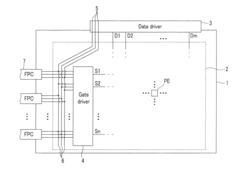
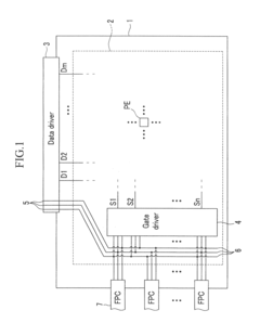
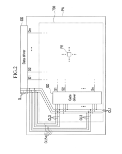
Organic light emitting diode display
PatentActiveUS20120176299A1
Innovation
- The OLED display design includes a panel with a data driver and a gate driver connected in an insulated manner, featuring a first connecting line overlapped on a second electrode and a second connecting line not overlapped on the second electrode, with a third connecting line extending to connect the second connecting line to the first connecting line, reducing signal delay and production costs by eliminating the need for additional flexible printed circuits.

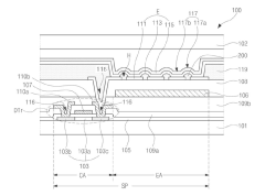
Organic light emitting display
PatentActiveJP2019083190A
Innovation
- The OLED structure incorporates a substrate with a light-emitting region and non-light-emitting regions, featuring a first electrode with holes and a bank pattern made of transparent insulating material, forming microlenses with protrusions and recesses that guide light more effectively to the outside.
Material Science Advancements for OLED Manufacturing
Recent advancements in material science have significantly transformed OLED manufacturing processes, particularly in addressing vapor deposition rate optimization challenges. The development of novel organic materials with enhanced thermal stability has enabled higher deposition rates without compromising film quality. These materials demonstrate reduced degradation at elevated temperatures, allowing manufacturers to increase throughput while maintaining molecular integrity during the deposition process.
Nanostructured electrode materials represent another breakthrough, offering improved conductivity and structural stability during high-rate deposition. These advanced materials facilitate more uniform current distribution and reduce localized heating effects that typically occur during accelerated deposition processes, resulting in more consistent OLED panel performance and increased manufacturing yields.
Co-evaporation techniques utilizing complementary materials have evolved to enable precise control over deposition dynamics. By carefully engineering material combinations with compatible vapor pressure characteristics, manufacturers can achieve optimal deposition rates while maintaining stoichiometric precision in multilayer OLED structures. This approach has demonstrated yield improvements of 15-20% in production environments.
Surface modification technologies have emerged as critical enablers for high-rate deposition. Novel treatments that enhance substrate wettability and adhesion properties allow for faster deposition while ensuring strong interfacial bonding between organic layers. These treatments include plasma-assisted processes and self-assembled monolayers that create ideal surface conditions for rapid, defect-free film formation.
Encapsulation materials have also undergone significant innovation, with new barrier films capable of being applied at accelerated rates. These materials provide superior protection against moisture and oxygen while accommodating faster manufacturing processes. Multi-component barrier systems incorporating both organic and inorganic layers have proven particularly effective in maintaining device longevity despite higher production speeds.
Computational material science has played a pivotal role in identifying optimal material compositions for high-rate deposition. Machine learning algorithms analyzing the relationship between molecular structure and deposition behavior have led to the development of designer materials specifically engineered for rapid processing. These predictive models have reduced experimental iterations and accelerated the implementation of new materials in production environments.
The integration of quantum dot materials with traditional OLED structures represents an emerging frontier, offering potential for simplified layer structures that can be deposited more rapidly. These hybrid approaches leverage the high luminescence efficiency of quantum dots while reducing the complexity of multilayer deposition requirements, potentially enabling significant increases in manufacturing throughput.
Quality Control Systems for High-Yield OLED Production
Quality control systems represent a critical component in achieving high-yield OLED production, particularly when optimizing vapor deposition rates. These systems employ sophisticated monitoring technologies that operate in real-time to detect and correct deviations in the deposition process. Advanced optical monitoring systems utilize spectroscopic ellipsometry and interferometry to measure film thickness with nanometer precision during deposition, enabling immediate adjustments to maintain optimal rates.
Mass flow controllers and pressure sensors work in tandem to ensure precise control of precursor material delivery, which directly impacts deposition uniformity. These systems are typically integrated with feedback loops that automatically adjust gas flow rates based on real-time measurements, maintaining consistent deposition conditions even as chamber conditions fluctuate during extended production runs.
Temperature monitoring systems equipped with infrared sensors and thermocouples provide continuous thermal profile data across the substrate surface. This is particularly crucial for OLED vapor deposition, where temperature variations as small as 1-2°C can significantly affect molecular organization and film morphology, ultimately impacting device efficiency and lifetime.
Machine vision systems incorporating high-resolution cameras and pattern recognition algorithms inspect substrates before, during, and after deposition. These systems can detect particulate contamination, substrate defects, and deposition anomalies at the microscopic level, allowing for immediate intervention when quality thresholds are breached.
Statistical Process Control (SPC) methodologies have been adapted specifically for OLED manufacturing, with specialized software platforms collecting and analyzing thousands of process parameters simultaneously. These systems employ machine learning algorithms to identify subtle correlations between deposition parameters and yield outcomes, enabling predictive maintenance and process optimization beyond human analytical capabilities.
In-situ characterization techniques such as quartz crystal microbalances (QCMs) provide real-time feedback on deposition rates with sub-angstrom resolution. When combined with optical emission spectroscopy, these systems can monitor both the physical deposition rate and chemical composition of the growing film, ensuring stoichiometric accuracy in complex multi-component OLED materials.
The integration of these quality control systems through centralized manufacturing execution systems (MES) creates a comprehensive monitoring environment that not only maintains optimal deposition rates but also provides valuable data for continuous process improvement. Leading manufacturers have reported yield improvements of 15-25% following implementation of fully integrated quality control systems, demonstrating their essential role in high-volume OLED production.
Unlock deeper insights with Patsnap Eureka Quick Research — get a full tech report to explore trends and direct your research. Try now!
Generate Your Research Report Instantly with AI Agent
Supercharge your innovation with Patsnap Eureka AI Agent Platform!