

How to Conduct OLED Surface Roughness Analysis for Quality
SEP 12, 20259 MIN READ
Generate Your Research Report Instantly with AI Agent
Patsnap Eureka helps you evaluate technical feasibility & market potential.
OLED Surface Roughness Analysis Background and Objectives
Organic Light-Emitting Diode (OLED) technology has revolutionized display and lighting industries since its commercial introduction in the late 1990s. The evolution of OLED technology has been marked by significant improvements in efficiency, lifetime, and manufacturing processes. Surface roughness analysis has emerged as a critical quality control parameter in OLED manufacturing, directly impacting device performance, optical properties, and long-term reliability.
The surface morphology of OLED layers plays a fundamental role in determining charge transport efficiency, light extraction capabilities, and overall device stability. Historically, surface roughness analysis techniques have evolved from basic optical microscopy to sophisticated atomic force microscopy (AFM) and white light interferometry methods, enabling nanometer-scale precision in surface characterization.
Current industry trends indicate a growing demand for higher resolution displays with improved color accuracy and energy efficiency, placing greater emphasis on precise surface quality control. The miniaturization of OLED pixels in high-density displays further necessitates advanced roughness analysis methodologies capable of detecting defects at increasingly smaller scales.
The primary objective of OLED surface roughness analysis is to establish standardized measurement protocols that can accurately quantify surface irregularities across multiple layers of the OLED stack. This includes the anode, hole transport layer, emissive layer, electron transport layer, and cathode, each requiring specific roughness parameters for optimal performance.
Secondary objectives include correlating surface roughness measurements with device performance metrics such as luminance efficiency, color uniformity, and operational lifetime. This correlation is essential for developing predictive models that can guide manufacturing process optimization and quality control procedures.
From a manufacturing perspective, the goal is to implement in-line, non-destructive surface roughness analysis techniques that can provide real-time feedback during production. This would enable immediate process adjustments, reducing waste and improving yield rates in high-volume manufacturing environments.
Research objectives focus on developing novel measurement techniques that can overcome current limitations in resolution, speed, and sample preparation requirements. Particular attention is being given to machine learning algorithms that can enhance the interpretation of roughness data and identify patterns indicative of potential device failure modes.
The ultimate aim is to establish a comprehensive understanding of how surface roughness at different interfaces within the OLED structure influences device physics, enabling the design of next-generation displays with superior performance characteristics and extended operational lifetimes.
Market Demand for High-Quality OLED Display Surfaces
The global OLED display market has witnessed substantial growth in recent years, driven by increasing consumer demand for superior visual experiences across various electronic devices. Market research indicates that the OLED display market is projected to reach $48.8 billion by 2023, with a compound annual growth rate of 15.2% between 2018 and 2023. This remarkable growth underscores the critical importance of surface quality in OLED manufacturing processes.
Surface roughness has emerged as a key quality parameter in OLED production, directly impacting display performance, durability, and consumer satisfaction. Industry data reveals that even nanometer-scale surface irregularities can significantly affect light emission uniformity, color accuracy, and overall display lifetime. Manufacturers who can consistently deliver smoother OLED surfaces gain substantial competitive advantages in premium device segments.
Consumer electronics companies, particularly smartphone and television manufacturers, are increasingly specifying stringent surface roughness requirements in their component sourcing. Market surveys indicate that end-users can visually detect quality differences between displays with varying surface roughness profiles, even without technical knowledge. This consumer sensitivity has translated into measurable market preferences, with devices featuring superior display surfaces commanding price premiums of 15-20% in high-end market segments.
The automotive industry represents another rapidly expanding market for high-quality OLED displays, with projected integration in 65% of premium vehicles by 2025. In this sector, surface quality requirements are particularly demanding due to harsh operating environments and extended product lifecycles. Automotive-grade OLEDs must maintain visual performance despite temperature fluctuations, vibration, and prolonged UV exposure—all factors directly influenced by initial surface roughness characteristics.
Medical imaging and professional creative industries constitute smaller but highly profitable market segments with exceptionally stringent surface quality demands. In medical applications, display surface imperfections can potentially compromise diagnostic accuracy, while design professionals require absolute color fidelity and uniformity for their work.
Market analysis reveals regional variations in OLED surface quality demands, with East Asian markets showing higher sensitivity to display performance metrics. This regional preference has influenced global manufacturing standards, as companies compete to meet the expectations of these discerning consumer bases.
The growing trend toward foldable and flexible OLED displays introduces additional surface quality challenges, as mechanical stress can amplify the visual impact of surface irregularities. Market forecasts suggest that flexible display technologies will represent 35% of the premium smartphone segment by 2024, creating urgent demand for advanced surface roughness analysis and control methodologies.
Current Challenges in OLED Surface Roughness Measurement
Despite significant advancements in OLED technology, surface roughness measurement remains a critical challenge in quality control processes. Current measurement techniques face several limitations that impact accuracy, efficiency, and integration into production environments. Conventional methods such as atomic force microscopy (AFM) and scanning electron microscopy (SEM) provide high-resolution data but are time-consuming, expensive, and often require destructive sample preparation, making them unsuitable for high-throughput manufacturing environments.
Optical profilometry and white light interferometry offer non-contact alternatives but struggle with the multi-layer structure of OLED displays, where light reflection from different interfaces can create measurement artifacts. These techniques also face challenges in distinguishing between actual surface roughness and subsurface defects, leading to potential misinterpretation of quality issues.
Real-time monitoring presents another significant hurdle, as most current technologies cannot be effectively integrated into production lines for in-situ measurements. This creates a disconnect between manufacturing processes and quality control, often resulting in delayed detection of defects and increased waste. The industry lacks standardized measurement protocols specifically designed for OLED surface characteristics, leading to inconsistencies in quality assessment across manufacturers.
Resolution limitations also persist, particularly as OLED pixel densities continue to increase. Many existing tools struggle to accurately characterize nanoscale roughness features that can significantly impact device performance and lifetime. This becomes especially problematic for flexible OLED displays, where surface deformation during bending creates additional measurement complexities.
Data processing and interpretation represent further challenges, as the correlation between measured surface parameters and actual device performance remains incompletely understood. Engineers often rely on empirical approaches rather than standardized metrics, making quality control decisions subjective and difficult to validate across different production batches.
Cost considerations also limit widespread implementation of advanced measurement technologies, particularly for smaller manufacturers. High-precision equipment requires substantial capital investment and specialized expertise for operation and maintenance, creating barriers to comprehensive quality control implementation throughout the supply chain.
Environmental factors such as temperature fluctuations, vibrations, and contamination can significantly impact measurement accuracy, necessitating strictly controlled conditions that are difficult to maintain in production environments. These challenges collectively highlight the need for innovative approaches to OLED surface roughness analysis that balance precision with practicality in manufacturing settings.
Established Methodologies for OLED Surface Roughness Assessment
01 Surface roughness control methods for OLED substrates
Various methods are employed to control the surface roughness of OLED substrates, which is critical for device performance. These methods include polishing techniques, planarization processes, and specialized coating methods that help achieve optimal smoothness. Controlling substrate roughness prevents electrical shorts, improves light extraction efficiency, and ensures uniform film deposition in subsequent manufacturing steps.- Surface roughness control methods for OLED substrates: Various methods are employed to control the surface roughness of OLED substrates, which is critical for device performance. These methods include polishing techniques, planarization processes, and specialized coating methods that can reduce surface irregularities. Controlling substrate roughness helps to ensure uniform light emission, prevent electrical shorts, and extend device lifetime by providing a smooth foundation for subsequent OLED layers.
- Impact of surface roughness on OLED efficiency and lifetime: Surface roughness significantly affects OLED performance parameters including efficiency, brightness uniformity, and operational lifetime. Rough surfaces can cause uneven electric field distribution, leading to localized high-current areas that accelerate degradation. Studies show that reducing surface roughness can improve light extraction efficiency, decrease pixel defects, and enhance overall device stability by minimizing stress points in the organic layers.
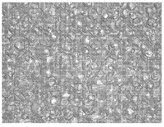
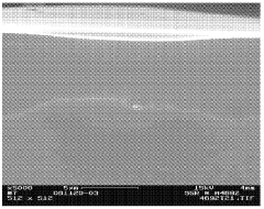
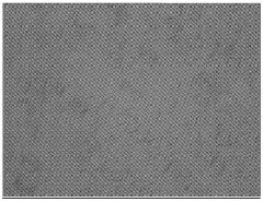
- Measurement and characterization of OLED surface roughness: Specialized techniques and instruments are used to measure and characterize surface roughness in OLED manufacturing. These include atomic force microscopy (AFM), optical profilometry, and scanning electron microscopy (SEM). Quantitative parameters such as root mean square (RMS) roughness and peak-to-valley measurements help manufacturers establish quality control standards and optimize production processes to achieve desired surface properties.
- Surface roughness modification for enhanced light extraction: Controlled surface roughness modification can be intentionally implemented to improve light extraction efficiency in OLEDs. By introducing specific micro or nano-scale textures on certain layers, internal light reflection can be reduced, allowing more light to escape from the device. These engineered surface structures can increase external quantum efficiency without compromising electrical performance, resulting in brighter displays with lower power consumption.
- Multilayer structures to compensate for surface roughness: Advanced multilayer structures are designed to compensate for substrate surface roughness in OLED devices. These include buffer layers, planarization films, and gradient-index materials that can effectively smooth out underlying irregularities. Such intermediate layers help to prevent the propagation of surface defects through the device stack, ensuring uniform electrical characteristics and preventing catastrophic shorts that would otherwise reduce manufacturing yield and device reliability.
02 Impact of surface roughness on OLED performance and lifetime
Surface roughness significantly affects OLED device performance and operational lifetime. Smoother surfaces lead to more uniform light emission, better electrical characteristics, and enhanced device stability. Excessive roughness can cause non-uniform current distribution, localized heating, and accelerated degradation of organic materials, ultimately reducing device efficiency and lifespan.Expand Specific Solutions03 Measurement and characterization techniques for OLED surface roughness
Advanced techniques are used to measure and characterize surface roughness in OLED manufacturing. These include atomic force microscopy (AFM), scanning electron microscopy (SEM), optical profilometry, and interferometry methods. These measurement techniques provide quantitative data on surface topography at nanometer scales, enabling precise quality control during production.Expand Specific Solutions04 Electrode surface roughness optimization for OLEDs
The surface roughness of electrodes (both anode and cathode) plays a crucial role in OLED performance. Optimizing electrode roughness improves charge injection, reduces contact resistance, and enhances light outcoupling efficiency. Various deposition methods and post-treatment processes are employed to achieve the ideal electrode surface profile for specific OLED applications.Expand Specific Solutions05 Novel materials and structures to mitigate surface roughness effects
Innovative materials and structural designs are being developed to mitigate the negative effects of surface roughness in OLEDs. These include buffer layers, planarization materials, nanostructured interfaces, and composite electrode materials. These approaches help accommodate inherent substrate roughness while maintaining optimal electrical and optical properties of the OLED device.Expand Specific Solutions
Leading Companies in OLED Quality Control Instrumentation
The OLED surface roughness analysis market is currently in a growth phase, driven by increasing demand for high-quality OLED displays across consumer electronics and automotive sectors. The global market size is estimated to exceed $500 million, expanding at a CAGR of approximately 12% as manufacturers prioritize quality control in production processes. Technologically, the field is moderately mature but evolving rapidly, with key players including Samsung Display, LG Display, and BOE Technology leading innovation through advanced metrology solutions. These companies have developed proprietary surface analysis techniques that combine atomic force microscopy with machine learning algorithms to detect nanoscale defects. Other significant contributors include Japan Display and TCL China Star Optoelectronics, who are investing heavily in automated inspection systems to improve yield rates and display performance.
BOE Technology Group Co., Ltd.
Technical Solution: BOE Technology has developed an integrated surface roughness analysis platform specifically for OLED manufacturing quality control. Their system employs laser scanning confocal microscopy as the primary measurement technique, complemented by atomic force microscopy for higher resolution verification. BOE's approach emphasizes high-throughput screening, with automated measurement stations positioned at critical points in the production line. Their proprietary analysis software calculates multiple roughness parameters including Ra, Rz, and bearing ratio curves to provide comprehensive surface characterization. The company has established correlation models between surface roughness metrics and key performance indicators such as luminance uniformity and pixel lifetime. BOE implements a statistical process control framework that continuously monitors roughness trends to detect process drift before it impacts yield. Their quality standards specify maximum allowable roughness values for each layer in the OLED stack, with particularly stringent requirements (Ra < 0.6nm) for the light-emitting layers. The company has also pioneered non-contact optical methods that can assess surface quality without risking damage to delicate OLED structures.
Strengths: High-throughput screening capability suitable for mass production; comprehensive statistical process control framework enables proactive quality management; non-contact measurement options protect sensitive OLED surfaces. Weaknesses: Primary reliance on optical techniques may miss certain nanoscale defects; system optimization focuses on production speed sometimes at the expense of ultimate resolution; requires regular calibration to maintain measurement accuracy.
Samsung Display Co., Ltd.
Technical Solution: Samsung Display has developed advanced Atomic Force Microscopy (AFM) techniques specifically optimized for OLED surface roughness analysis. Their approach combines high-resolution AFM with proprietary image processing algorithms to detect nanoscale defects and variations in OLED layers. The company employs a multi-parameter characterization system that measures not only Ra (average roughness) but also Rq (root mean square roughness) and Rmax (maximum height difference) values to comprehensively evaluate surface quality. Samsung has integrated in-line monitoring systems that can perform real-time surface analysis during production, using white light interferometry alongside AFM for faster throughput. Their quality control protocol establishes strict roughness thresholds (typically maintaining Ra values below 0.5nm for critical layers) to ensure optimal light emission properties and prevent pixel defects. The company has also pioneered correlation studies between surface roughness measurements and final device performance metrics, creating predictive models that allow for early intervention in the manufacturing process.
Strengths: Industry-leading resolution capabilities down to sub-nanometer level; integrated real-time monitoring systems reduce production delays; comprehensive multi-parameter analysis provides deeper insights than single-metric approaches. Weaknesses: Proprietary equipment requires significant capital investment; high-precision measurements can be time-consuming compared to faster but less accurate methods; requires highly trained operators for optimal results.
Critical Technologies in Nanoscale Surface Characterization
Method for manufacturing a structure with a textured surface for an organic light-emitting diode device, and structure with a textured surface
PatentWO2010112786A2
Innovation
- A method for manufacturing a textured surface on a mineral glass substrate with controlled roughness, using a smoothing layer of silica to soften the surface and enhance light extraction while maintaining reliability, involving a sol-gel deposition process that is cost-effective and applicable on large surfaces.
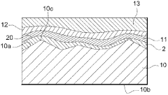
Method for producing a structure with a textured external surface, intended for an organic light-emitting diode device, and a structure with a textured external surface
PatentInactiveEP2415098A2
Innovation
- A method for manufacturing a textured external surface on a mineral glass substrate with randomly arranged submicron protrusions and hollows, using a mask deposition and etching process, followed by a softening step to control surface roughness and prevent electrical degradation, ensuring a wide band of wavelength extraction and improved reliability.
Industry Standards and Certification Requirements
The OLED industry operates under a comprehensive framework of standards and certifications that govern surface roughness analysis and quality control. The International Electrotechnical Commission (IEC) has established IEC 62341 series specifically for OLED displays, with subsections addressing surface quality requirements including roughness parameters. These standards typically specify acceptable Ra (average roughness) values below 1.0 nm for high-quality OLED substrates and functional layers.
The International Organization for Standardization (ISO) provides complementary standards through ISO 25178 for surface texture measurement, which has become the reference point for 3D surface roughness analysis in OLED manufacturing. These standards define measurement methodologies, calibration procedures, and reporting formats to ensure consistency across the industry.
In the United States, SEMI (Semiconductor Equipment and Materials International) has developed standards specific to display manufacturing that include surface quality metrics. SEMI MS8 addresses surface roughness measurement for flat panel displays, providing guidelines for both measurement techniques and acceptable tolerance ranges for different display applications.
The Japanese Electronics and Information Technology Industries Association (JEITA) has established ED-2522 standards specifically for OLED display quality assessment, including surface roughness parameters. These standards are particularly influential in Asian manufacturing centers where much of global OLED production is concentrated.
Certification requirements vary by market region, with the European Union requiring CE marking that indirectly references surface quality through performance and reliability metrics. Similarly, UL certification in North America includes durability testing that can be affected by surface roughness characteristics. The Korean Certificate (KC) and China Compulsory Certificate (CCC) both include specific requirements for display quality that reference surface characteristics.
For manufacturers, compliance with these standards typically requires documented measurement procedures using calibrated equipment traceable to national measurement institutes. Quality management systems like ISO 9001 require regular auditing of measurement processes, including surface roughness analysis. Third-party certification bodies such as TÜV, SGS, and Intertek provide verification services to ensure compliance with relevant standards.
The trend in certification requirements is moving toward more stringent surface roughness specifications as OLED technology advances into applications like foldable displays and automotive interfaces, where surface defects can have more significant impacts on performance and longevity.
Cost-Benefit Analysis of Advanced Surface Inspection Systems
When evaluating the implementation of advanced surface inspection systems for OLED surface roughness analysis, a comprehensive cost-benefit analysis is essential to justify the investment. The initial capital expenditure for high-precision inspection equipment typically ranges from $250,000 to $2 million, depending on the technology sophistication, resolution capabilities, and throughput capacity.
Operational costs must also be factored in, including maintenance contracts (approximately 10-15% of initial equipment cost annually), specialized training for operators ($5,000-$10,000 per technician), and potential production line modifications to accommodate the inspection systems ($50,000-$150,000). Energy consumption and facility requirements represent additional ongoing expenses that vary based on system specifications.
Against these costs, manufacturers must weigh significant quantifiable benefits. Quality improvement metrics indicate that advanced inspection systems can reduce defect escape rates by 85-95% compared to traditional methods. This translates to a substantial decrease in customer returns and warranty claims, with industry data suggesting savings of $15-25 per panel produced.
Production yield improvements represent perhaps the most compelling economic benefit. Manufacturers implementing advanced surface roughness analysis systems report yield increases of 5-12%, which for high-volume production can result in millions of dollars in additional revenue annually. The ability to detect and address surface anomalies earlier in the production process prevents value-added operations on defective components.
Time-to-market advantages also provide competitive benefits that, while more difficult to quantify precisely, significantly impact market positioning. Early detection of systematic surface issues can accelerate process optimization by 30-40%, reducing development cycles for new OLED products.
Return on investment calculations typically show breakeven periods of 12-24 months for mid-range systems, with premium systems requiring 18-36 months to reach ROI. However, these calculations often underestimate long-term benefits such as enhanced brand reputation and customer confidence resulting from consistent quality.
For manufacturers considering implementation, a phased approach often provides the optimal balance between immediate quality improvements and capital preservation. Beginning with critical inspection points and expanding coverage as ROI is demonstrated allows for more manageable investment cycles while still capturing significant quality benefits.
Unlock deeper insights with Patsnap Eureka Quick Research — get a full tech report to explore trends and direct your research. Try now!
Generate Your Research Report Instantly with AI Agent
Supercharge your innovation with Patsnap Eureka AI Agent Platform!