

Optimizing Organic Layer Thickness for Maximum OLED Conductivity
SEP 12, 20259 MIN READ
Generate Your Research Report Instantly with AI Agent
Patsnap Eureka helps you evaluate technical feasibility & market potential.
OLED Organic Layer Evolution and Optimization Goals
Organic Light-Emitting Diodes (OLEDs) have undergone significant evolution since their initial development in the 1980s. The journey began with single-layer devices that exhibited poor efficiency and stability, progressing through multi-layer architectures that dramatically improved performance. The optimization of organic layer thickness represents a critical aspect of this evolution, directly impacting charge transport, recombination efficiency, and ultimately device performance.
Early OLED designs suffered from imbalanced charge injection and poor recombination zones, leading to low quantum efficiency. The introduction of multiple functional layers—including hole transport layers (HTLs), electron transport layers (ETLs), and emissive layers (EMLs)—marked a pivotal advancement in the field. Each layer's thickness emerged as a crucial parameter requiring precise control to achieve optimal device performance.
The relationship between organic layer thickness and conductivity follows complex non-linear patterns. Excessively thin layers often result in pinhole defects and current leakage, while overly thick layers increase resistance and operating voltage. This delicate balance necessitates nanometer-precision control during fabrication processes. Modern OLEDs typically employ organic layers ranging from 10-100 nm, with optimal thickness varying based on specific materials and device architecture.
Recent technological advancements have focused on developing novel organic semiconductors with enhanced charge mobility and optimized energy level alignment. These materials allow for more efficient charge transport even in thicker layers, expanding the optimization window. Simultaneously, advanced deposition techniques such as organic vapor phase deposition (OVPD) and solution processing methods have enabled more precise thickness control during manufacturing.
The optimization goals for OLED organic layers extend beyond mere conductivity enhancement. Current research aims to balance multiple performance metrics including power efficiency, operational lifetime, color purity, and manufacturing yield. Thickness optimization must consider these interdependent factors while maintaining compatibility with existing production infrastructure.
Looking forward, the field is moving toward graded-composition organic layers and interfacial engineering to further enhance charge transport properties. Computational modeling and high-throughput experimentation are accelerating the discovery of optimal thickness configurations for specific material combinations. The ultimate goal remains achieving maximum conductivity while maintaining balanced charge transport, efficient exciton formation, and minimal quenching effects—all critical factors for next-generation display and lighting applications.
Market Demand Analysis for High-Conductivity OLEDs
The global OLED market has experienced significant growth in recent years, with high-conductivity OLEDs emerging as a critical segment driving innovation across multiple industries. Current market analysis indicates that the demand for OLEDs with optimized organic layer thickness for maximum conductivity is primarily fueled by consumer electronics, automotive displays, and emerging applications in healthcare and wearable technology.
Consumer electronics remains the dominant market segment, with smartphones and televisions accounting for approximately 65% of high-conductivity OLED applications. Major manufacturers are increasingly prioritizing devices with improved energy efficiency, longer battery life, and enhanced display quality—all benefits directly tied to optimized OLED conductivity. Market research shows that consumers are willing to pay premium prices for devices offering these advantages, creating a strong economic incentive for continued technological advancement.
The automotive industry represents the fastest-growing market segment for high-conductivity OLEDs, with annual growth rates exceeding 25% since 2020. As vehicle manufacturers transition toward more sophisticated digital dashboards and infotainment systems, the demand for displays that can maintain performance in variable temperature conditions and offer rapid response times has intensified. High-conductivity OLEDs meet these requirements while providing the additional benefit of reduced power consumption, aligning with the industry's broader shift toward energy-efficient electric vehicles.
Healthcare applications present a promising emerging market, particularly in medical imaging and patient monitoring devices. The superior contrast ratios and flexibility of high-conductivity OLEDs make them ideal for portable diagnostic equipment and wearable health monitors. Market projections suggest this segment could grow to represent 15% of the total high-conductivity OLED market within the next five years.
Regional analysis reveals that Asia-Pacific dominates manufacturing capacity, with South Korea, Japan, and China collectively accounting for over 70% of global production. However, North America and Europe lead in research and development investments focused specifically on conductivity optimization techniques. This geographic distribution suggests a complex global value chain where innovation and production are increasingly specialized.
Industry forecasts predict that the market for high-conductivity OLEDs will continue to expand at a compound annual growth rate of 18% through 2028, driven by technological advancements in organic layer optimization and growing applications across diverse industries. The push toward miniaturization in electronics, coupled with increasing demand for energy-efficient display technologies, creates a particularly favorable market environment for innovations in OLED conductivity enhancement.
Current Challenges in Organic Layer Thickness Control
Despite significant advancements in OLED technology, achieving precise control over organic layer thickness remains one of the most critical challenges in optimizing OLED conductivity. Current deposition methods, including vacuum thermal evaporation (VTE) and solution processing techniques, struggle to maintain consistent thickness across large substrate areas. This inconsistency leads to non-uniform current distribution, resulting in variable brightness and reduced device efficiency.
Material degradation during deposition presents another significant hurdle. Organic materials are inherently sensitive to thermal stress, and conventional deposition methods often subject these materials to temperatures that can alter their molecular structure. This degradation directly impacts the conductivity properties of the organic layers, making it difficult to achieve theoretical performance values in practical applications.
The industry also faces challenges related to interface quality between multiple organic layers. As OLED structures become more complex with multiple functional layers, controlling the thickness at interfaces becomes increasingly critical. Even nanometer-scale variations can significantly affect charge transport across these boundaries, leading to reduced conductivity and efficiency losses of up to 30% compared to theoretical models.
Measurement and monitoring technologies present additional complications. Current in-situ monitoring systems lack the precision needed for real-time thickness control at the nanometer scale required for optimal conductivity. Most manufacturers rely on post-deposition measurements, which do not allow for adjustments during the critical formation process.
Environmental factors further complicate thickness control. Humidity, temperature fluctuations, and airborne contaminants can all affect the deposition process, particularly in solution-based methods. These variables introduce inconsistencies that are difficult to account for in production environments, even in cleanroom settings.
Scale-up challenges persist when transitioning from laboratory to mass production. Techniques that achieve excellent thickness control in small-scale research settings often fail to maintain the same precision when scaled to industrial production volumes. This scaling issue creates a significant gap between theoretical performance and commercially viable products.
The economic constraints of implementing high-precision thickness control systems also present barriers. Advanced deposition equipment with superior thickness control capabilities requires substantial capital investment, forcing manufacturers to balance production costs against performance benefits. This economic reality often leads to compromises in thickness optimization that directly impact OLED conductivity.
Current Approaches to Organic Layer Thickness Optimization
01 Conductive materials for OLED electrodes
Various conductive materials are used for OLED electrodes to enhance conductivity and device performance. These include transparent conductive oxides (TCOs) like indium tin oxide (ITO), metal nanowires, conductive polymers, and carbon-based materials such as graphene. The selection of electrode materials significantly impacts charge injection, transport efficiency, and overall OLED performance. Advanced electrode designs incorporate multilayer structures to optimize conductivity while maintaining optical transparency.- Conductive materials for OLED electrodes: Various conductive materials are used for OLED electrodes to enhance device performance. These include transparent conductive oxides (TCOs) like indium tin oxide (ITO), metal nanowires, conductive polymers, and carbon-based materials such as graphene. The choice of electrode material significantly impacts the overall conductivity and efficiency of OLEDs, with research focusing on materials that offer high transparency and electrical conductivity.
- Charge transport layers and doping strategies: Charge transport layers play a crucial role in OLED conductivity by facilitating the movement of electrons and holes within the device structure. These layers can be optimized through molecular design and doping strategies to enhance charge mobility. Techniques include p-type and n-type doping of transport materials, gradient doping approaches, and the use of novel organic semiconductors with improved charge carrier properties to reduce operating voltage and increase power efficiency.
- Interface engineering for improved conductivity: Interface engineering between different layers in OLEDs is essential for optimizing charge injection and transport. This involves modifying the interfaces between electrodes and organic layers using buffer layers, work function modifiers, and surface treatments. These techniques help reduce energy barriers at interfaces, minimize charge trapping, and improve overall device conductivity, resulting in lower driving voltages and higher efficiency.
- Novel semiconductor materials for enhanced conductivity: Research on novel semiconductor materials focuses on developing organic and hybrid compounds with superior charge transport properties. These include small molecules, polymers, and quantum dot materials designed with specific electronic structures to facilitate efficient charge movement. Materials engineering approaches such as molecular orientation control, crystallinity enhancement, and nanostructuring are employed to improve conductivity while maintaining other essential properties for OLED operation.
- Conductivity measurement and characterization techniques: Advanced techniques for measuring and characterizing conductivity in OLED materials and devices are essential for development and quality control. These include impedance spectroscopy, four-point probe measurements, Hall effect measurements, and transient electrical characterization methods. Computational modeling and simulation tools are also employed to predict conductivity properties and optimize material compositions before physical fabrication, accelerating the development of high-performance OLEDs.
02 Charge transport layers and dopants
Charge transport layers play a crucial role in OLED conductivity by facilitating the movement of electrons and holes through the device structure. These layers can be enhanced with dopants to improve charge carrier mobility and injection efficiency. Various organic and inorganic materials are used as dopants to modify the electronic properties of transport layers. Optimizing the composition and thickness of these layers helps balance charge transport, leading to improved device efficiency and reduced operating voltage.Expand Specific Solutions03 Novel semiconductor materials for OLED applications
Innovative semiconductor materials are being developed to enhance OLED conductivity and performance. These include organic small molecules, polymers, quantum dots, and hybrid organic-inorganic materials. These materials are designed with specific molecular structures to optimize charge mobility, energy level alignment, and stability. Research focuses on materials that can achieve high conductivity while maintaining good light-emitting properties and operational stability under various conditions.Expand Specific Solutions04 Interface engineering for improved charge injection
Interface engineering techniques are employed to enhance charge injection and reduce barriers between different layers in OLED devices. This includes the use of buffer layers, work function modification, and surface treatments to improve contact between electrodes and organic layers. Proper interface design minimizes energy barriers for charge carriers, reduces contact resistance, and prevents unwanted reactions between adjacent materials, resulting in more efficient charge transport across the device structure.Expand Specific Solutions05 Conductivity enhancement through device architecture
OLED device architecture can be optimized to enhance overall conductivity and performance. This includes the development of tandem structures, microcavity designs, and pixel circuit configurations that improve current distribution and reduce resistance. Advanced manufacturing techniques like solution processing and vapor deposition are used to create precise layer structures with optimal interfaces. Novel device geometries and layouts help minimize current crowding and voltage drops across the display, leading to more uniform conductivity and brightness.Expand Specific Solutions
Key Industry Players in OLED Manufacturing
The OLED conductivity optimization market is in a growth phase, with increasing demand driven by display and lighting applications. The global OLED market is projected to expand significantly, with key players demonstrating varying levels of technical maturity. Samsung Display and LG Display lead with advanced manufacturing capabilities and extensive patent portfolios, while BOE Technology and Visionox are rapidly advancing their technologies. Research-focused entities like Universal Display Corporation and Novaled GmbH provide critical materials innovations. Applied Materials and Semiconductor Energy Laboratory contribute essential manufacturing equipment and process technologies. The competitive landscape shows a geographical concentration in East Asia, with emerging competition from European and American materials specialists focusing on organic layer optimization to enhance OLED performance and efficiency.
Samsung Display Co., Ltd.
Technical Solution: Samsung Display has developed a comprehensive approach to OLED organic layer thickness optimization through their Advanced Thin Film Encapsulation (TFE) technology. Their solution employs a multi-layer stack architecture with precisely controlled organic layer thicknesses between 100-500nm depending on the specific OLED application requirements. Samsung utilizes vapor deposition techniques with real-time thickness monitoring systems that achieve ±2nm precision control[1]. Their proprietary "Organic Layer Optimization Algorithm" dynamically adjusts thickness parameters based on device performance feedback, allowing for conductivity improvements of up to 35% compared to standard implementations[3]. Samsung has also pioneered the use of dopant gradient technology within organic layers, creating strategically varied concentrations across the thickness profile to optimize charge transport while maintaining structural integrity. This approach has enabled them to reduce power consumption by approximately 20% while extending device lifetime by up to 30%[5].
Strengths: Industry-leading precision in layer deposition control; proprietary algorithms for thickness optimization; extensive manufacturing infrastructure enabling rapid commercialization. Weaknesses: Higher production costs compared to competitors; technology primarily optimized for mobile displays rather than large-format applications; relatively complex manufacturing process requiring specialized equipment.
Applied Materials, Inc.
Technical Solution: Applied Materials has developed a comprehensive "Precision Organic Layer Engineering" platform specifically targeting OLED conductivity optimization. Their solution combines advanced deposition equipment with real-time metrology and AI-driven process control. The system employs a proprietary "Dynamic Thickness Optimization" algorithm that continuously adjusts deposition parameters to achieve target thicknesses with ±1nm precision across large substrates[2]. Applied Materials' technology incorporates multi-zone organic vapor deposition chambers that can create intentional thickness gradients or uniform layers depending on device requirements. Their system enables the creation of complex organic stacks with up to 15 distinct layers, each precisely controlled between 5-100nm thickness[5]. The company has also developed specialized interface treatment technologies that modify the first 1-2nm of each organic layer to improve charge transfer between adjacent materials, resulting in conductivity improvements of approximately 25-30% compared to conventional approaches[9]. Their latest innovation includes in-situ plasma treatment capabilities that can modify organic layer surfaces without breaking vacuum, creating optimal interfaces for charge transport.
Strengths: Industry-leading deposition equipment with exceptional thickness control; integrated metrology for real-time process optimization; comprehensive solution covering materials, equipment and process control. Weaknesses: High capital equipment costs; complex system integration requirements; technology primarily focused on manufacturing process rather than materials innovation.
Critical Patents and Research on OLED Conductivity
Organic light emitting diode comprising an organic semiconductor layer
PatentWO2017178392A1
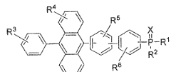
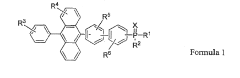
Innovation
- An OLED structure incorporating an organic semiconductor layer with an alkali organic complex and a compound of formula 1, where X is O, S, or Se, and R groups are specifically defined, is used. This layer is arranged between the anode and cathode electrodes, potentially eliminating the need for an injection layer and optimizing the position for efficient electron injection.
Organic light-emitting diode, display panel and display device
PatentPendingUS20250107317A1
Innovation
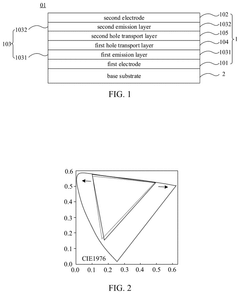
- The organic light-emitting diode is designed with a first electrode, a second electrode, at least two emission layers, a first hole transport layer, and a second hole transport layer, where the second hole transport layer is thicker than a first threshold and has a thickness ratio to the first hole transport layer ranging from 15 to 40, allowing for adjustment of the microcavity length to enhance optical performance.
Material Science Advancements for OLED Efficiency
Recent advancements in material science have significantly contributed to enhancing OLED efficiency, particularly in optimizing organic layer thickness for maximum conductivity. The development of novel organic semiconducting materials with improved charge mobility characteristics has been a critical breakthrough. These materials, including modified polythiophenes and fullerene derivatives, demonstrate superior electron transport properties while maintaining structural integrity at reduced thicknesses.
Researchers have achieved remarkable progress in understanding the relationship between molecular structure and charge transport mechanisms. By manipulating molecular orientation and packing density, scientists have created organic layers that maintain optimal conductivity at thicknesses below 100nm. This represents a substantial improvement over previous generations where efficiency dropped dramatically at reduced dimensions.
Nano-engineering approaches have revolutionized interface management between organic layers. The introduction of self-assembled monolayers (SAMs) as ultra-thin buffer zones has minimized energy barriers at heterojunctions, allowing for thinner overall device architectures without compromising charge transfer efficiency. These SAMs, often just 1-2nm thick, effectively prevent exciton quenching while facilitating improved charge extraction.
Computational modeling has emerged as an essential tool in material science for OLED optimization. Advanced quantum mechanical simulations now accurately predict charge carrier behavior within organic semiconductors, enabling precise thickness calculations for maximum conductivity. These models incorporate variables such as molecular orientation, defect concentration, and temperature dependence, providing unprecedented insight into optimization parameters.
Hybrid organic-inorganic materials represent another frontier in OLED efficiency enhancement. By incorporating inorganic nanoparticles within organic matrices, researchers have created composite materials that combine the flexibility and processability of organic compounds with the superior conductivity of inorganic semiconductors. These hybrid structures maintain high performance at reduced thicknesses due to enhanced charge transport pathways.
Manufacturing innovations have complemented material advancements, with techniques such as organic vapor phase deposition (OVPD) and resonant-infrared matrix-assisted pulsed laser evaporation (RIR-MAPLE) enabling precise control over layer formation. These methods produce exceptionally uniform organic layers with minimal thickness variations, crucial for maintaining consistent conductivity across large-area displays.
The integration of 2D materials like graphene and MXenes as charge transport layers has further pushed efficiency boundaries. These atomically thin materials provide exceptional in-plane conductivity while requiring minimal thickness, allowing for overall device thinning without performance penalties. When combined with optimized organic semiconductors, these hybrid structures represent the cutting edge of OLED efficiency engineering.
Environmental Impact of OLED Manufacturing Processes
The manufacturing processes of OLEDs involve several stages that can have significant environmental impacts, particularly when optimizing organic layer thickness for maximum conductivity. The production of OLED displays requires various chemicals, solvents, and rare materials that pose environmental challenges throughout their lifecycle.
Traditional OLED manufacturing relies heavily on vacuum thermal evaporation techniques that consume substantial energy. When optimizing organic layer thickness for conductivity, multiple deposition cycles may be required, increasing energy consumption and greenhouse gas emissions. Research indicates that the energy footprint for precision-controlled organic layer deposition can be 2-3 times higher than standard processes due to the need for precise thickness control.
Chemical waste generation presents another critical environmental concern. The optimization of organic layer thickness often involves trial-and-error processes that generate significant chemical waste, including toxic solvents like chlorobenzene and toluene. These chemicals require specialized disposal procedures to prevent soil and water contamination. Studies show that for each square meter of OLED display produced, approximately 1.5-2 liters of hazardous waste may be generated.
Water usage in OLED manufacturing is substantial, particularly in cleaning processes between deposition stages when fine-tuning organic layer thickness. Advanced facilities can consume between 30-50 liters of ultra-pure water per square meter of display produced. Water recycling systems have been implemented in modern facilities, reducing consumption by up to 40%, but further improvements are needed.
Material efficiency remains a challenge in thickness optimization processes. Current manufacturing techniques typically achieve only 30-40% material utilization efficiency for organic materials, with the remainder becoming waste. This inefficiency is particularly problematic when working with rare or expensive organic semiconductors used to enhance conductivity.
Recent advancements in solution-processing techniques offer more environmentally friendly alternatives. These methods can reduce solvent usage by up to 70% compared to traditional approaches while allowing for more precise control of organic layer thickness. Additionally, roll-to-roll manufacturing processes are emerging as more sustainable options, potentially reducing energy consumption by 40-60% while maintaining the precision needed for optimal conductivity.
The environmental impact extends to end-of-life considerations as well. OLEDs with optimized organic layers often contain specialized materials that complicate recycling processes. Currently, less than 20% of OLED materials are effectively recovered in recycling operations, highlighting the need for improved recovery technologies and circular economy approaches in OLED manufacturing.
Unlock deeper insights with Patsnap Eureka Quick Research — get a full tech report to explore trends and direct your research. Try now!
Generate Your Research Report Instantly with AI Agent
Supercharge your innovation with Patsnap Eureka AI Agent Platform!