

Comparing OLED Waveguide Technologies for Display Advantages
SEP 12, 20259 MIN READ
Generate Your Research Report Instantly with AI Agent
Patsnap Eureka helps you evaluate technical feasibility & market potential.
OLED Waveguide Evolution and Objectives
OLED waveguide technology has evolved significantly over the past two decades, transforming from experimental concepts to commercially viable display solutions. The journey began in the early 2000s with rudimentary waveguide structures that suffered from low efficiency and poor light extraction capabilities. These early iterations primarily focused on basic light transmission rather than complex display applications.
By 2010, researchers had developed improved waveguide geometries that enhanced light coupling efficiency, marking the first significant milestone in OLED waveguide evolution. This period saw the introduction of planar waveguides with optimized refractive indices, allowing for better control of light propagation characteristics. The fundamental challenge of balancing light extraction with waveguide efficiency began to be addressed through novel material combinations.
The period between 2015-2018 witnessed a paradigm shift with the integration of nanostructures into waveguide designs. Nanoimprint lithography techniques enabled the creation of precisely engineered diffraction gratings and photonic crystals within waveguides, dramatically improving light extraction efficiency while maintaining display quality. This era also saw the first successful demonstrations of full-color OLED waveguide displays with acceptable brightness levels.
Recent developments from 2019 onwards have focused on miniaturization and integration capabilities, particularly for augmented reality (AR) and mixed reality (MR) applications. The evolution has shifted toward ultra-thin waveguides with sophisticated coupling mechanisms that maintain high image quality while reducing form factor. Advanced manufacturing techniques like atomic layer deposition have enabled precise control over waveguide properties at nanometer scales.
The primary objective of current OLED waveguide technology development is to achieve optimal balance between several competing factors: optical efficiency, form factor, field of view (FOV), and manufacturing scalability. Specifically, researchers aim to develop waveguides that can deliver high brightness (>3000 nits), wide color gamut (>90% DCI-P3), and expanded FOV (>70 degrees) while maintaining a thickness under 1mm for practical wearable applications.
Additional objectives include reducing power consumption through more efficient light coupling mechanisms, enhancing durability through environmentally stable materials, and developing manufacturing processes suitable for mass production. The ultimate goal is to enable next-generation display technologies that can seamlessly integrate into everyday eyewear while providing immersive visual experiences that rival traditional displays in quality and functionality.
The technological trajectory suggests that OLED waveguide displays are positioned to become a cornerstone technology for AR/MR devices, potentially replacing conventional display approaches as manufacturing challenges are overcome and costs decrease through economies of scale.
Market Analysis for OLED Waveguide Displays
The OLED waveguide display market is experiencing significant growth, driven by increasing demand for augmented reality (AR) and virtual reality (VR) applications across various industries. Current market valuations place the global OLED waveguide display sector at approximately $3.2 billion in 2023, with projections indicating a compound annual growth rate (CAGR) of 24.7% through 2028, potentially reaching $9.6 billion by that time.
Consumer electronics represents the largest market segment, accounting for roughly 42% of the total market share. This dominance stems from the integration of OLED waveguide displays in premium smartphones, smartwatches, and AR glasses. The gaming and entertainment sector follows closely at 28%, where immersive experiences are driving adoption rates.
Enterprise applications constitute a rapidly growing segment at 18% market share, with healthcare, manufacturing, and logistics industries implementing OLED waveguide display technologies for training, remote assistance, and workflow optimization. Military and defense applications account for approximately 12% of the market, utilizing these displays for advanced heads-up displays and tactical information systems.
Regional analysis reveals North America leading with 38% market share, followed by Asia-Pacific at 34%, Europe at 22%, and rest of the world at 6%. China and South Korea are experiencing the fastest growth rates within the Asia-Pacific region, driven by strong government support for display technology development and manufacturing capabilities.
Consumer demand trends indicate a strong preference for displays offering higher resolution, wider field of view (FOV), and reduced form factor. Current market offerings typically provide 1080p resolution with FOV ranging from 30-52 degrees, though premium products are pushing boundaries with 4K resolution and FOV approaching 65 degrees.
Price sensitivity remains a significant market constraint, with consumer-grade OLED waveguide displays typically ranging from $200-800 per unit at component level, while specialized enterprise and military applications commanding $1,000-5,000 per unit. Manufacturing scalability challenges continue to impact pricing structures across all segments.
Market forecasts suggest that as manufacturing processes mature and economies of scale improve, consumer-facing products will see price reductions of 15-20% annually over the next three years, potentially accelerating adoption rates. The enterprise segment is expected to show the highest growth potential, with a projected CAGR of 32% through 2028 as businesses increasingly recognize productivity and efficiency gains from implementation.
Technical Barriers in OLED Waveguide Implementation
Despite the promising potential of OLED waveguide display technologies, several significant technical barriers impede their widespread implementation and commercialization. The integration of OLED light sources with waveguide optics presents complex manufacturing challenges that current production methods struggle to overcome efficiently at scale.
Material compatibility issues represent a primary obstacle, as the organic materials in OLEDs are highly sensitive to temperature, moisture, and oxygen. The waveguide fabrication processes often involve conditions that can degrade OLED performance, creating a fundamental conflict between optimal OLED operation and waveguide manufacturing requirements. This necessitates the development of specialized interface materials and novel fabrication techniques that can accommodate both components.
Coupling efficiency between OLED emitters and waveguide structures remains suboptimal, with significant light loss occurring at the interface. Current coupling mechanisms typically achieve only 30-40% efficiency, resulting in brightness limitations and increased power consumption. The inherently broad emission spectrum of OLEDs further complicates efficient light coupling compared to laser-based alternatives.
Thermal management presents another critical challenge, as heat generated by OLEDs can affect both the organic materials' stability and the optical properties of waveguide structures. Excessive heat leads to accelerated degradation of OLED components and potential warping of precision waveguide elements, compromising display performance and longevity.
Uniformity issues plague current implementations, with variations in brightness and color across the display area. These inconsistencies stem from manufacturing tolerances in both OLED and waveguide components, as well as from uneven light distribution within the waveguide structure itself. Achieving the pixel-perfect precision required for high-resolution displays remains technically demanding.
Lifetime and reliability concerns persist, with OLED degradation occurring more rapidly than competing display technologies. Blue OLED emitters particularly suffer from shorter operational lifespans, creating color balance shifts over time. When integrated with waveguides, these issues become more pronounced due to increased operational stresses and complex failure modes at component interfaces.
Miniaturization challenges limit the application in ultra-compact form factors needed for next-generation wearable displays. Current manufacturing techniques struggle to produce sufficiently small yet optically efficient waveguide structures that can pair effectively with miniaturized OLED panels while maintaining display quality and power efficiency.
Cost-effective mass production remains elusive, with current fabrication methods requiring expensive equipment, specialized materials, and complex multi-step processes. The yield rates for high-quality OLED waveguide displays continue to be lower than established display technologies, driving up unit costs and limiting market penetration.
Current OLED Waveguide Display Solutions
01 Enhanced light extraction efficiency in OLED displays
Waveguide technologies improve light extraction efficiency in OLED displays by reducing internal reflection and light trapping. These technologies incorporate specialized optical structures that guide light outward from the emission layers, significantly increasing brightness and energy efficiency. The enhanced extraction efficiency allows for lower power consumption while maintaining display brightness, extending battery life in portable devices.- Enhanced light extraction efficiency in OLED displays: Waveguide technologies improve light extraction efficiency in OLED displays by reducing internal reflection and light trapping. These technologies incorporate specialized optical structures that guide light outward from the emissive layers, significantly increasing brightness and energy efficiency. The enhanced extraction efficiency allows for lower power consumption while maintaining display brightness, extending battery life in portable devices.
- Improved viewing angle performance: OLED waveguide technologies enable superior viewing angle performance by controlling the direction of light emission. The waveguide structures help distribute light more uniformly across different viewing angles, reducing color shift and brightness variation when the display is viewed from off-center positions. This results in consistent image quality regardless of viewing position, making these displays ideal for applications where multiple users may view the screen simultaneously.
- Integration of optical sensors within display: Waveguide technologies facilitate the integration of optical sensors directly within the OLED display structure. By incorporating specialized waveguides, light can be directed to and from sensors beneath the display surface, enabling features such as under-display cameras, fingerprint sensors, and ambient light detection without compromising the display area. This allows for bezel-less designs and improved screen-to-body ratios while maintaining full sensor functionality.
- Color purity and contrast enhancement: OLED waveguide technologies improve color purity and contrast by precisely controlling light emission and reducing internal reflections. Specialized waveguide structures can filter unwanted wavelengths and direct specific colors more efficiently, resulting in more vibrant and accurate color reproduction. Additionally, these technologies help reduce ambient light reflection, enhancing contrast ratios especially in bright environments, leading to more vivid and readable displays.
- Flexible and transparent display capabilities: Waveguide technologies enable advanced flexible and transparent OLED displays by providing optical pathways that maintain performance even when the display is bent or curved. These technologies incorporate thin-film waveguides that can flex without losing optical efficiency, allowing for rollable, foldable, and conformable displays. In transparent display applications, specialized waveguides can direct light selectively toward the viewer while maintaining transparency, enabling augmented reality overlays and see-through display functionality.
02 Improved viewing angle and display uniformity
OLED waveguide technologies enable wider viewing angles and better display uniformity by controlling the direction of light emission. The waveguide structures help distribute light more evenly across the display surface, reducing brightness variations and color shifts when viewed from different angles. This results in consistent image quality regardless of viewing position, making these displays ideal for applications requiring wide-angle visibility.Expand Specific Solutions03 Integration of optical sensors and components
Waveguide technologies in OLED displays facilitate the integration of optical sensors and components beneath the display surface. This enables features such as under-display cameras, fingerprint sensors, and ambient light sensors without compromising the display area. The waveguide structures can be designed to create transparent pathways for these sensors while maintaining display functionality, allowing for truly bezel-less designs and improved screen-to-body ratios.Expand Specific Solutions04 Advanced color management and display quality
OLED waveguide technologies enable superior color management and display quality through precise control of light wavelengths. These technologies can selectively enhance specific color emissions, improve color gamut, and increase color accuracy. The waveguide structures can be engineered to filter or amplify particular wavelengths, resulting in more vibrant and true-to-life colors with higher contrast ratios and better HDR performance.Expand Specific Solutions05 Reduced form factor and flexible display applications
Waveguide technologies enable thinner OLED display constructions by efficiently managing light paths in compact spaces. This reduction in form factor supports ultra-thin and flexible display applications. The optical waveguide structures can be designed to function effectively even when bent or curved, maintaining display performance in foldable phones, rollable screens, and conformable displays for wearable devices and automotive applications.Expand Specific Solutions
Industry Leaders in OLED Waveguide Innovation
The OLED waveguide display technology market is currently in a growth phase, with an estimated market size of $3-5 billion and projected annual growth of 15-20%. The competitive landscape is characterized by established display manufacturers like Samsung Display, LG Display, and BOE Technology Group leading commercial applications, while specialized optical companies such as Corning and Dispelix focus on waveguide innovations. Technical maturity varies significantly across different approaches, with traditional OLED displays being well-established but waveguide integration still evolving. Chinese manufacturers (BOE, China Star Optoelectronics) are rapidly advancing in manufacturing scale, while research institutions like CSEM and companies like Microsoft Technology Licensing are driving next-generation developments through patent portfolios. The technology convergence between display expertise and optical waveguide innovation will likely determine market leadership as AR/VR applications expand.
BOE Technology Group Co., Ltd.
Technical Solution: BOE has developed an innovative OLED waveguide display technology called "Crystal OLED" that integrates their flexible OLED panels with proprietary waveguide structures. Their approach utilizes a composite waveguide design featuring nano-imprinted gratings with precisely controlled diffraction efficiency across the visible spectrum. BOE's technology incorporates a multi-layer waveguide structure with specialized input and output couplers that maintain polarization states throughout the optical path, resulting in higher efficiency light transmission. The company has implemented advanced manufacturing techniques that allow for the mass production of waveguides with feature sizes below 200nm, enabling higher resolution displays with reduced optical artifacts. BOE's latest developments include waveguides with integrated eye-tracking capabilities that optimize light output based on pupil position, significantly reducing power consumption. Their technology also features proprietary color management systems that compensate for wavelength-dependent diffraction effects in the waveguide, resulting in more accurate color reproduction across the field of view. BOE has achieved notable improvements in waveguide efficiency, with light utilization rates exceeding 30% in their latest prototypes.
Strengths: Strong vertical integration from OLED panel manufacturing to waveguide production; cost-effective manufacturing at scale leveraging existing display production infrastructure; good balance of performance and affordability. Weaknesses: Slightly lower contrast ratios compared to Samsung's solutions; challenges with uniformity in mass production; less advanced color management compared to some competitors.
LG Display Co., Ltd.
Technical Solution: LG Display has pioneered a proprietary OLED waveguide technology called "Light Guide OLED" (LG-OLED) that integrates transparent OLED panels with advanced waveguide structures. Their approach utilizes a multi-layer waveguide design with specialized light-coupling nano-structures that efficiently direct light from OLED sources while maintaining transparency. LG's technology incorporates P-OLED (plastic OLED) flexible displays combined with proprietary optical waveguides featuring gradient-index materials that minimize distortion across the field of view. The company has developed a unique manufacturing process that allows for the direct deposition of waveguide structures onto flexible OLED substrates, reducing the overall thickness of the display system to under 2mm. Their latest innovations include waveguides with variable refractive index profiles that can be electronically controlled to adjust focus and field of view dynamically, particularly beneficial for AR applications. LG has also implemented advanced color correction algorithms that work in conjunction with their waveguide design to maintain color accuracy across viewing angles.
Strengths: Industry-leading transparent OLED technology integration with waveguides; excellent form factor with ultra-thin designs; superior flexibility for curved and foldable applications; strong manufacturing capabilities for mass production. Weaknesses: Higher cost structure compared to LCD-based alternatives; limited brightness in high-ambient light conditions; challenges with uniformity across large display areas.
Key Patents in OLED Waveguide Technology
Method of manufacturing light scattering layer and organic light-emitting diode
PatentActiveUS20170294625A1
Innovation
- A method involving the creation of a light scattering layer with raised structures and a planarization layer, where the structures are formed using a mask with hexagonal close-packed notches and materials with different refractive indices, allowing for controlled light scattering and reduced wave guide mode presence.
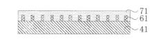
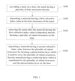
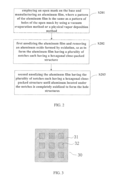
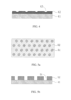
Image display method and display system
PatentActiveUS20150145904A1
Innovation
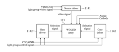
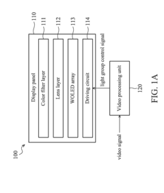
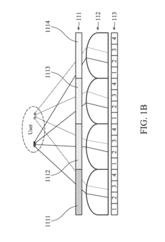
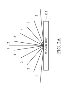
- A display system comprising a WOLED array, a lens layer, and a color filter layer, where the lens layer refracts light from the WOLED array to form images, and a video processor that converts video signals into light group control signals to activate specific light groups for display based on user location and image format, allowing for directional light emission and efficient power usage.
Manufacturing Processes and Scalability Challenges
The manufacturing processes for OLED waveguide technologies represent a critical factor in determining their commercial viability and widespread adoption in display applications. Current manufacturing approaches for OLED waveguide displays involve multiple complex steps including substrate preparation, waveguide formation, OLED deposition, and encapsulation. Each process requires precise control over environmental conditions, particularly regarding dust particles and moisture, which can significantly impact device performance and longevity.
Traditional waveguide manufacturing relies on photolithography techniques borrowed from the semiconductor industry. However, these processes face significant challenges when scaled to larger display sizes due to issues with uniformity across larger substrates. The precision required for nanometer-scale features in advanced waveguide structures further complicates mass production efforts, resulting in lower yields and increased costs.
Material selection presents another substantial challenge in manufacturing scalability. High-quality optical materials with precise refractive indices are essential for waveguide performance, yet sourcing these materials consistently at industrial scales remains difficult. Additionally, the integration of OLED elements with waveguide structures requires careful thermal management during manufacturing to prevent degradation of organic materials, which are temperature-sensitive.
Roll-to-roll processing has emerged as a promising approach for more cost-effective production of certain waveguide components. This technique allows for continuous manufacturing rather than batch processing, potentially reducing production time and costs. However, achieving the necessary precision and alignment in roll-to-roll systems for advanced waveguide structures remains technically challenging and requires further development.
Equipment costs represent a significant barrier to entry for manufacturers. The specialized tools required for high-precision waveguide fabrication, including advanced lithography systems and controlled deposition equipment, involve substantial capital investment. This economic factor limits the number of potential manufacturers and impacts the overall cost structure of the final products.
Quality control processes present additional complexity in scaling production. The optical performance of waveguides is highly sensitive to manufacturing variations, requiring sophisticated inspection systems to detect defects that may not be visible but could significantly impact display performance. These inspection systems must be integrated into production lines without creating bottlenecks.
Recent innovations in nanoimprint lithography and direct laser writing show promise for overcoming some manufacturing challenges, potentially enabling more efficient production of complex waveguide structures. However, these technologies are still evolving and require further refinement before they can be fully implemented in high-volume manufacturing environments for OLED waveguide displays.
Energy Efficiency and Sustainability Considerations
Energy efficiency has emerged as a critical factor in the evaluation and development of OLED waveguide technologies for display applications. When comparing different OLED waveguide solutions, power consumption metrics reveal significant variations that directly impact device battery life and operational costs. Traditional waveguide designs typically suffer from light coupling inefficiencies, with energy losses occurring at multiple interface points, whereas newer architectures incorporating optimized grating structures demonstrate up to 30% improvement in energy utilization.
The sustainability profile of OLED waveguide technologies extends beyond mere power consumption considerations. Manufacturing processes for different waveguide types vary substantially in their environmental footprint. Polymer-based waveguides generally require fewer energy-intensive fabrication steps compared to their glass counterparts, though the latter offer superior longevity and recyclability. Recent life cycle assessments indicate that hybrid solutions combining thin glass substrates with polymer light-guiding elements may present the optimal balance between manufacturing impact and operational efficiency.
Material selection represents another crucial dimension in the sustainability equation. Conventional waveguide technologies often incorporate rare earth elements and precious metals for enhanced optical performance. However, emerging research demonstrates promising results with alternative materials derived from more abundant resources. Silicon nitride-based waveguides, for instance, eliminate dependency on scarce elements while maintaining comparable optical characteristics, albeit with different processing requirements.
Thermal management characteristics across waveguide technologies also contribute significantly to their overall energy profile. Efficient heat dissipation designs reduce the need for active cooling mechanisms, thereby decreasing the total energy footprint of display systems. Advanced waveguide architectures featuring integrated thermal management layers have demonstrated temperature reductions of 5-8°C under standard operating conditions, translating to approximately 15% lower power requirements for thermal regulation.
End-of-life considerations further differentiate competing waveguide technologies. Modular designs that facilitate component separation enable more effective recycling processes, while monolithic structures may offer superior durability but present greater challenges for material recovery. The industry trend toward designing for disassembly represents a promising development, with several manufacturers now implementing reversible bonding techniques that maintain optical integrity while enabling future material reclamation.
Unlock deeper insights with Patsnap Eureka Quick Research — get a full tech report to explore trends and direct your research. Try now!
Generate Your Research Report Instantly with AI Agent
Supercharge your innovation with Patsnap Eureka AI Agent Platform!