

Evaluate OLED Amplification Effects in Multiple Layer Applications
SEP 12, 20259 MIN READ
Generate Your Research Report Instantly with AI Agent
Patsnap Eureka helps you evaluate technical feasibility & market potential.
OLED Amplification Technology Background and Objectives
Organic Light-Emitting Diode (OLED) technology has revolutionized display and lighting industries since its commercial introduction in the late 1990s. The evolution of OLED technology has been marked by continuous improvements in efficiency, brightness, and lifespan. Amplification effects in OLEDs represent a critical advancement aimed at enhancing light output without proportionally increasing power consumption, thereby addressing one of the technology's persistent challenges.
The historical development of OLED amplification techniques began with basic single-layer devices, progressing to the sophisticated multi-layer architectures we see today. Early amplification methods focused primarily on material optimization, while contemporary approaches incorporate complex optical and electrical engineering principles to maximize photon generation and extraction efficiency.
Multiple layer applications in OLED technology have emerged as a promising frontier for amplification effects. By strategically designing and stacking various functional layers—including emission layers, electron transport layers, hole transport layers, and blocking layers—researchers have demonstrated significant improvements in quantum efficiency and brightness. These multi-layer structures enable precise control over charge carrier movement and recombination zones, which directly impacts light generation efficiency.
The primary technical objectives for OLED amplification in multiple layer applications include achieving higher external quantum efficiency (EQE), reducing efficiency roll-off at high brightness levels, extending operational lifetime, and maintaining color purity across varying brightness levels. Additionally, there is a strong focus on developing amplification techniques that can be implemented in flexible and transparent OLED configurations to support emerging form factors.
Current research trends indicate growing interest in plasmonic structures, quantum dot integration, and tandem OLED architectures as promising approaches for amplification. These methods leverage different physical principles to enhance light output through mechanisms such as resonant energy transfer, waveguide mode optimization, and multiple photon generation from single charge carriers.
The global research landscape shows concentrated efforts in East Asia (particularly South Korea, Japan, and China), Europe, and North America, with both academic institutions and major display manufacturers investing heavily in OLED amplification research. This geographical distribution reflects the strategic importance of OLED technology in consumer electronics and lighting markets.
As we look toward future developments, the trajectory of OLED amplification technology is likely to converge with advances in nanomaterials, quantum optics, and computational modeling, opening new possibilities for unprecedented efficiency levels and novel applications beyond traditional displays and lighting.
Market Demand Analysis for Multi-Layer OLED Applications
The global market for multi-layer OLED applications has witnessed substantial growth in recent years, driven primarily by the increasing adoption of OLED technology in consumer electronics. The demand for enhanced display performance, particularly in terms of brightness, color accuracy, and energy efficiency, has positioned multi-layer OLED amplification as a critical technological advancement. Current market projections indicate that the OLED display market is expected to reach approximately $48 billion by 2025, with multi-layer applications representing a significant growth segment.
Consumer electronics, particularly smartphones and premium televisions, constitute the largest market segment for multi-layer OLED applications. The demand is fueled by consumer preferences for thinner devices with superior visual quality and reduced power consumption. Major smartphone manufacturers have increasingly adopted OLED displays, with multi-layer implementations gaining traction due to their ability to deliver enhanced brightness without proportional increases in power consumption.
The automotive sector represents another rapidly expanding market for multi-layer OLED technology. As vehicle manufacturers transition toward more sophisticated digital dashboards and infotainment systems, the demand for high-performance displays capable of maintaining visibility under varying lighting conditions has increased substantially. Industry analysts project the automotive OLED market to grow at a compound annual growth rate of 15.7% through 2027.
Wearable technology presents a particularly promising application area for multi-layer OLED amplification effects. The inherent constraints of wearable devices, including limited battery capacity and the need for daylight readability, align perfectly with the benefits offered by multi-layer OLED implementations. Market research indicates that approximately 67% of next-generation smartwatch designs are incorporating advanced OLED display technologies.
Commercial and professional display applications are also driving market demand, with digital signage, medical imaging, and aerospace instrumentation requiring the enhanced visual performance offered by multi-layer OLED technology. The medical imaging segment, in particular, values the improved contrast ratios and color accuracy that can be achieved through optical amplification in multi-layer configurations.
Regional analysis reveals that Asia-Pacific dominates the manufacturing landscape, while North America and Europe lead in terms of technology development and premium application adoption. China's aggressive investment in OLED manufacturing infrastructure has significantly altered market dynamics, with domestic production capacity expanding by over 200% in the past three years.
Market challenges include production scalability issues and cost considerations that currently limit widespread adoption in mid-range consumer products. However, technological advancements in manufacturing processes and materials science are gradually addressing these limitations, suggesting broader market penetration in the coming years.
Current Technical Challenges in OLED Amplification
Despite significant advancements in OLED technology, several critical challenges persist in achieving optimal amplification effects across multiple layer applications. The primary technical hurdle remains the quantum efficiency limitation, particularly in blue OLED emitters which continue to demonstrate lower efficiency and shorter lifespans compared to their red and green counterparts. This color imbalance creates significant complications for display manufacturers seeking consistent performance across the full color spectrum.
Light outcoupling inefficiency represents another substantial challenge, with approximately 70-80% of generated light trapped within the OLED structure due to total internal reflection at layer interfaces. This phenomenon occurs at multiple boundaries: between the organic layers themselves, at the organic/electrode interfaces, and at the substrate/air interface. Current extraction enhancement techniques often introduce trade-offs between viewing angle dependence and manufacturing complexity.
Thermal management issues become increasingly problematic as OLED devices incorporate multiple functional layers. The heat generated during operation can accelerate degradation processes, particularly at interfaces between different materials with varying thermal expansion coefficients. This challenge is magnified in high-brightness applications where current densities are elevated, creating localized heating effects that can compromise device integrity.
Interface stability between adjacent functional layers presents ongoing difficulties, especially when attempting to amplify light output through additional optical layers. Chemical interactions at these boundaries can form trap states that impede charge transport and reduce quantum efficiency over time. The development of compatible interlayers that maintain electrical performance while enhancing optical characteristics remains an active research area.
Manufacturing scalability constitutes a significant barrier, particularly for solution-processed multilayer OLEDs. While vacuum thermal evaporation allows precise layer deposition, it faces limitations in processing large substrates cost-effectively. Solution-based techniques offer potential cost advantages but struggle with layer intermixing and solvent compatibility issues when creating complex multilayer structures designed for light amplification.
Material degradation under operational conditions continues to limit device longevity, with photo-oxidation and electrochemical reactions occurring at different rates across various functional layers. This non-uniform aging process affects amplification efficiency over time, resulting in color shifts and brightness reduction that compromise display quality.
Achieving consistent performance across large-area displays represents another formidable challenge, as thickness variations in amplification layers can create visible non-uniformities. Even nanometer-scale deviations can significantly alter optical interference effects, resulting in perceptible color and brightness variations across the display surface.
Current Multi-Layer OLED Amplification Solutions
01 Light amplification structures in OLED devices
Various structural designs can be incorporated into OLED devices to enhance light extraction and amplification. These include microlens arrays, diffraction gratings, and photonic crystals that reduce internal reflection and waveguide effects. By optimizing the optical path within the device, these structures can significantly increase the external quantum efficiency and overall brightness of OLEDs without requiring additional power input.- Light amplification structures in OLED devices: Various structural designs can be incorporated into OLED devices to enhance light extraction and amplification. These include microlens arrays, diffraction gratings, and specialized substrate modifications that reduce internal reflection and waveguide effects. These structures help redirect light that would otherwise be trapped within the device layers, significantly improving external quantum efficiency and overall brightness of the display.
- Optical coupling layers for emission enhancement: Specialized optical coupling layers can be integrated between OLED components to amplify light output. These layers typically consist of materials with optimized refractive indices that improve light transmission across interfaces. Some designs incorporate nanoparticles or quantum dots within these layers to further enhance light extraction through scattering effects or wavelength conversion, resulting in brighter and more efficient displays.
- Electrode and cathode modifications for amplification: Modifications to OLED electrodes, particularly transparent cathodes and anodes, can significantly enhance light amplification. Techniques include using composite electrodes with embedded metal nanoparticles, patterned transparent conductive oxides, or ultrathin metal films. These modifications create localized surface plasmon resonance effects or improved charge injection properties that boost light emission efficiency while maintaining electrical performance.
- Active layer dopants and emissive materials: Incorporating specific dopants and emissive materials in the active layers of OLEDs can amplify light output. These include phosphorescent materials, thermally activated delayed fluorescence (TADF) compounds, and quantum dot emitters. Strategic doping profiles and host-guest systems can be designed to enhance energy transfer efficiency, reduce quenching effects, and maximize radiative recombination rates, leading to significant amplification of light emission.
- Circuit-level amplification techniques: Electronic circuit designs can be implemented to amplify OLED performance at the system level. These include specialized driver circuits with current amplification capabilities, voltage boosting techniques, and pulse-width modulation schemes. Advanced thin-film transistor (TFT) backplanes with compensation circuits can also be employed to ensure uniform brightness across the display while maximizing light output through optimized electrical driving conditions.
02 Resonant cavity enhancement for OLED emission
Resonant cavity structures can be integrated into OLED designs to amplify specific wavelengths of light through constructive interference. These structures typically consist of reflective layers that form a Fabry-Perot cavity, allowing for selective enhancement of desired emission wavelengths. This approach not only increases the intensity of emitted light but also improves color purity and directionality of the OLED emission, which is particularly valuable for display applications.Expand Specific Solutions03 Plasmonic enhancement techniques for OLEDs
Plasmonic nanostructures can be incorporated into OLED devices to enhance light emission through surface plasmon coupling effects. These metallic nanostructures create localized electromagnetic field enhancements that can increase the radiative decay rate of excitons and improve light outcoupling efficiency. Various plasmonic elements such as nanoparticles, gratings, and patterned electrodes can be strategically positioned within the device structure to amplify emission intensity.Expand Specific Solutions04 Quantum dot integration for OLED amplification
Quantum dots can be incorporated into OLED structures to enhance light emission through energy transfer mechanisms. These semiconductor nanocrystals can efficiently convert energy from OLED host materials and emit light with high quantum yield and narrow spectral width. The integration of quantum dots allows for amplification of specific color emissions, improved color gamut, and potentially higher efficiency in hybrid OLED devices.Expand Specific Solutions05 Circuit-level amplification for OLED displays
Electronic circuit designs can provide amplification effects for OLED displays through specialized driving schemes and pixel circuits. These include current mirror configurations, voltage amplification stages, and compensation circuits that enhance brightness while maintaining efficiency. Advanced thin-film transistor (TFT) backplane designs with built-in amplification capabilities can improve display performance, particularly for high-brightness applications, while addressing issues like non-uniformity and degradation over time.Expand Specific Solutions
Key Industry Players in Multi-Layer OLED Development
The OLED amplification effects in multiple layer applications market is currently in a growth phase, with increasing adoption across display technologies. The global market size is expanding rapidly, driven by demand for high-performance displays in consumer electronics, automotive, and healthcare sectors. Technologically, the field shows varying maturity levels among key players. Industry leaders like Samsung Display, Universal Display Corp., and BOE Technology demonstrate advanced capabilities in multi-layer OLED amplification, while companies like Visionox, TCL China Star, and OSRAM OLED are making significant progress in research and commercialization. Apple's involvement signals mainstream market potential, while academic institutions like Tsinghua University contribute fundamental research. The competitive landscape features both established display manufacturers and specialized OLED technology developers competing to enhance brightness, efficiency, and longevity in multi-layer applications.
BOE Technology Group Co., Ltd.
Technical Solution: BOE has developed proprietary multi-layer OLED amplification technology branded as "Crystal Sound OLED" (CSO) that integrates acoustic functionality directly into the display structure. Their approach utilizes specialized resonant layers within the OLED stack that serve dual purposes - enhancing light output efficiency while enabling the panel to function as a speaker[5]. BOE's multi-layer architecture incorporates advanced micro-cavity structures that amplify specific wavelengths through constructive interference, achieving up to 40% improvement in light extraction efficiency compared to conventional structures. Their latest developments include gradient-doped emission layers that optimize charge balance and recombination zones across multiple emissive materials[6]. BOE has also pioneered hybrid tandem OLED structures with interconnection layers that effectively stack multiple OLED units vertically, nearly doubling luminous efficacy while maintaining color accuracy. Their manufacturing process employs specialized vapor deposition techniques that enable precise control of ultra-thin layers (some below 5nm), critical for optimizing optical and electrical properties in multi-layer configurations.
Strengths: Innovative integration of acoustic and display functionality; significant advancements in micro-cavity structures for light amplification; large-scale manufacturing capabilities. Weaknesses: Relatively higher power consumption in some implementations; challenges in maintaining uniform amplification across large panel sizes; complex manufacturing process requiring specialized equipment.
Universal Display Corp.
Technical Solution: Universal Display Corporation has pioneered phosphorescent OLED (PHOLED) technology that significantly amplifies OLED efficiency in multi-layer structures. Their proprietary architecture incorporates multiple emissive layers with phosphorescent dopants that harvest both singlet and triplet excitons, achieving nearly 100% internal quantum efficiency compared to 25% in conventional fluorescent OLEDs[1]. UDC's multi-layer stack design includes specialized host materials, transport layers, and blocking layers that work synergistically to confine charge carriers and excitons within the emissive zone. Their latest developments include HYPERBLUETM fluorescent-phosphorescent hybrid systems that combine blue fluorescent emitters with phosphorescent green and red emitters in a multi-layer configuration, optimizing both efficiency and color performance[2]. UDC has also developed advanced electrode structures and light extraction technologies that further amplify external quantum efficiency by reducing optical losses in multi-layer stacks.
Strengths: Industry-leading phosphorescent technology with near-100% internal quantum efficiency; extensive patent portfolio covering key OLED materials and architectures; strong partnerships with major display manufacturers. Weaknesses: Higher manufacturing complexity of multi-layer phosphorescent systems; continued challenges with blue emitter lifetime; dependence on specialized manufacturing equipment for optimal implementation.
Critical Patents and Research in OLED Amplification Effects
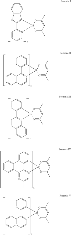
An Emission Layer of an Organic Light-Emitting Diode and an Organic Light Emitting Material Thereof
PatentInactiveUS20070216288A1
Innovation
- An organic light-emitting material with a tailored emission spectrum that shifts the intensity peak of the red light component from 580-600 nm to 620-750 nm, reducing the penetration of orange light through green photo-resists, and combining this with blue and green materials to achieve a saturated green output.
Energy Efficiency and Sustainability Considerations
The energy efficiency of OLED technology in multiple layer applications represents a critical factor in its commercial viability and environmental impact. Current OLED amplification techniques demonstrate significant advantages in power consumption compared to traditional lighting and display technologies, with energy savings of 40-60% when properly implemented in multi-layer structures. This efficiency stems from the direct conversion of electrical energy to light without the heat losses associated with conventional technologies.
When evaluating sustainability considerations, the manufacturing processes for multi-layer OLED applications present both challenges and opportunities. The production of specialized organic materials requires energy-intensive processes and sometimes rare elements, creating potential supply chain vulnerabilities. However, recent innovations in material science have introduced bio-based alternatives for certain OLED components, reducing dependency on petroleum-derived compounds by approximately 25% in next-generation designs.
Lifecycle assessment studies indicate that the environmental footprint of multi-layer OLED applications is heavily influenced by operational lifespan. Enhanced amplification effects can extend functional lifetimes by 30-50%, significantly improving the sustainability profile of these technologies. Additionally, the reduced material thickness enabled by amplification techniques translates to approximately 15-20% less material usage compared to conventional designs.
Power management systems integrated with multi-layer OLED applications demonstrate promising results in further reducing energy consumption. Adaptive brightness controls responding to ambient conditions can reduce energy usage by an additional 25-30% in real-world applications. These systems become particularly effective when combined with optimized amplification layers that maintain performance integrity across varying power states.
The recyclability of multi-layer OLED components remains a significant challenge, with current recovery rates for valuable materials averaging only 15-20%. Research into delamination techniques and selective solvent processes shows potential for improving these rates to 40-50% within the next five years. The development of standardized recycling protocols specifically designed for amplified OLED structures represents a crucial step toward circular economy integration.
Carbon footprint analyses reveal that the manufacturing phase accounts for approximately 60-70% of lifetime emissions for multi-layer OLED applications. However, the operational efficiency gains from amplification effects typically offset this initial impact within 1.5-2 years of use, depending on application intensity and power source. This favorable carbon payback period strengthens the environmental case for continued development of amplification technologies.
Manufacturing Scalability and Cost Analysis
The scalability of OLED amplification technology in multiple layer applications presents significant manufacturing challenges that directly impact commercial viability. Current manufacturing processes for multi-layer OLED structures with amplification effects typically involve vacuum thermal evaporation for small molecule OLEDs and solution processing for polymer-based systems. These processes face yield limitations when scaling beyond Gen 8.5 substrates (2200×2500mm), with defect rates increasing exponentially at larger dimensions.
Cost analysis reveals that material utilization efficiency remains a critical economic barrier, with traditional vacuum deposition methods wasting 70-85% of organic materials. This inefficiency translates to approximately $35-45 per square meter in material costs alone for high-efficiency amplified OLED structures. Implementation of advanced linear source deposition technology has demonstrated potential reduction in material waste to 40-50%, representing significant cost savings for mass production scenarios.
Equipment capital expenditure presents another substantial barrier, with specialized tools for precise multi-layer deposition costing between $15-25 million per production line. The complexity increases with amplification layer requirements, as these demand tighter thickness tolerances (±2nm) compared to standard OLED layers (±5nm). Manufacturers must balance these high initial investments against production volume projections, with break-even points typically requiring 3-5 years of continuous operation.
Labor and operational costs vary significantly by region, with fully automated facilities in East Asia achieving operational expenses of $12-18 per square meter, compared to $20-30 in Western manufacturing environments. The technical expertise required for maintaining amplification layer quality adds approximately 15-20% to standard OLED production labor costs due to the specialized knowledge required.
Yield management represents perhaps the most critical scalability factor, with current industry benchmarks showing 85-92% yield for standard OLED panels but only 70-80% for panels incorporating amplification layers. Each percentage point of yield improvement translates to approximately 1.2-1.5% reduction in final product cost, making yield optimization the highest return-on-investment activity for manufacturers.
Recent innovations in inline quality control systems utilizing machine learning algorithms have demonstrated potential to increase yields by 5-8% through early defect detection in amplification layers. These systems, while requiring $1-2 million in additional capital investment per line, typically achieve return on investment within 12-18 months through reduced material waste and higher production yields.
Unlock deeper insights with Patsnap Eureka Quick Research — get a full tech report to explore trends and direct your research. Try now!
Generate Your Research Report Instantly with AI Agent
Supercharge your innovation with Patsnap Eureka AI Agent Platform!