

Optimize OLED Printing Methods for Uniform Brightness
SEP 12, 20259 MIN READ
Generate Your Research Report Instantly with AI Agent
Patsnap Eureka helps you evaluate technical feasibility & market potential.
OLED Printing Evolution and Brightness Uniformity Goals
Organic Light-Emitting Diode (OLED) technology has undergone significant evolution since its inception in the 1950s when electroluminescence in organic materials was first observed. The journey from laboratory curiosity to commercial display technology accelerated in the 1980s with Eastman Kodak's pioneering work on small molecule OLEDs. By the early 2000s, solution-processed OLEDs emerged as a promising alternative to vacuum deposition methods, offering potential cost advantages and scalability for large-area applications.
The printing methods for OLED fabrication have evolved through several distinct phases. Initially, spin-coating techniques dominated laboratory research but proved impractical for large-scale manufacturing. This limitation led to the development of inkjet printing for OLED materials around 2000, which offered precise deposition control but faced challenges with material viscosity and nozzle clogging. Subsequently, screen printing, gravure printing, and flexographic printing techniques were adapted for OLED production, each offering unique advantages in terms of throughput and resolution.
Brightness uniformity has emerged as a critical quality parameter in OLED displays and lighting panels. Non-uniform brightness manifests as visible variations across the display surface, degrading user experience and product value. Historical data indicates that early commercial OLED displays exhibited brightness variations exceeding 15% across the panel, whereas current industry standards typically require uniformity within 5% deviation for premium applications.
The technical goals for OLED printing optimization focus on several interconnected parameters. Primary among these is achieving pixel-to-pixel brightness variation of less than 3% across the entire printed area, which represents a significant challenge given the sensitivity of OLED materials to processing conditions. Secondary goals include maintaining this uniformity throughout the operational lifetime of the device, as differential aging can exacerbate initial non-uniformities.
Current research trajectories aim to develop printing methods that can simultaneously optimize material deposition thickness (target: ±2nm precision), lateral resolution (target: <10μm), and chemical purity preservation during the printing process. These parameters directly impact brightness uniformity through their effects on charge transport and recombination efficiency within the OLED stack.
The industry roadmap projects that by 2025, advanced printing techniques should achieve sub-1% brightness variation across panels up to Gen 8 size (2200×2500mm), representing a step-change improvement over current capabilities. This advancement would enable OLED technology to further penetrate premium display markets and expand into architectural lighting applications where uniformity expectations are particularly stringent.
Market Demand for High-Quality OLED Displays
The global OLED display market has witnessed substantial growth over the past decade, driven primarily by increasing consumer demand for superior visual experiences across various electronic devices. Current market valuations place the OLED display sector at approximately 40 billion USD, with projections indicating a compound annual growth rate of 14-16% through 2028. This robust growth trajectory underscores the critical importance of addressing manufacturing challenges such as brightness uniformity in OLED printing methods.
Consumer electronics represents the largest application segment for high-quality OLED displays, with smartphones alone accounting for over 50% of market demand. Major smartphone manufacturers have transitioned their flagship models to OLED technology, citing superior color reproduction, contrast ratios, and energy efficiency as primary motivators. Market research indicates that consumers are increasingly willing to pay premium prices for devices featuring high-quality displays, with brightness uniformity consistently ranking among the top three quality factors influencing purchasing decisions.
The automotive sector has emerged as a rapidly expanding market for OLED display technology, with luxury vehicle manufacturers incorporating these displays into dashboard systems and entertainment consoles. Industry analysts project that the automotive OLED market segment will grow at nearly 20% annually through 2027, outpacing the overall OLED market growth. Vehicle manufacturers specifically emphasize the need for displays with uniform brightness to ensure readability under variable lighting conditions and to maintain brand quality perceptions.
Television and large-format display markets continue to drive significant demand for advanced OLED printing methods. Premium television manufacturers have reported 30-35% year-over-year growth in OLED TV sales, despite higher retail prices compared to conventional LED technologies. Consumer feedback consistently highlights display uniformity as a critical factor in justifying the price premium of OLED televisions, with brightness inconsistencies being among the most commonly reported quality concerns.
Commercial applications including digital signage, retail displays, and professional monitors represent an expanding market segment with particularly stringent requirements for brightness uniformity. This sector values longevity and consistent performance, with procurement specifications typically mandating brightness uniformity tolerances of less than 5% deviation across the display surface. Market research indicates that commercial buyers are willing to invest 15-20% more in display technologies that can demonstrate superior uniformity metrics over extended operational periods.
Emerging applications in wearable technology, healthcare displays, and augmented reality systems are creating new demand vectors for high-quality OLED displays with exceptional brightness uniformity. These specialized applications often operate under challenging viewing conditions that amplify the visibility of any manufacturing inconsistencies, further emphasizing the market value of optimized OLED printing methods.
Current OLED Printing Techniques and Uniformity Challenges
The OLED (Organic Light-Emitting Diode) printing industry currently employs several key techniques for display manufacturing, each with distinct advantages and limitations regarding brightness uniformity. Inkjet printing represents one of the most widely adopted methods, offering precise deposition of organic materials through digitally controlled nozzles. This technique enables high-resolution patterning and efficient material usage, but faces challenges in maintaining consistent droplet size and preventing coffee ring effects that lead to brightness variations across the display.
Slot-die coating has emerged as another significant technique, particularly for larger area applications. This method provides continuous film deposition with good thickness control, though edge effects remain problematic for achieving uniform brightness, especially at display boundaries. The technique struggles with patterning complexity, limiting its application in high-resolution displays where pixel-level uniformity is critical.
Screen printing, while offering robust manufacturing capabilities for certain OLED components, exhibits limitations in resolution and layer thickness uniformity that directly impact brightness consistency. The mechanical contact nature of this process can introduce stress-related defects that manifest as brightness anomalies in the final display.
Current uniformity challenges span multiple dimensions of the manufacturing process. Material-related issues include viscosity fluctuations during printing, solvent evaporation rates that vary with environmental conditions, and molecular weight distribution inconsistencies that affect film formation. These factors collectively contribute to non-uniform light emission characteristics.
Process-related challenges present equally significant hurdles. Temperature gradients across substrates during thermal annealing create varying degrees of molecular organization, directly impacting charge transport and recombination efficiency. Mechanical alignment precision between successive printed layers remains difficult to maintain at scale, resulting in pixel misalignment that appears as brightness inconsistencies to end users.
Environmental factors further complicate uniformity control, with humidity variations affecting solvent evaporation rates and dust particles creating defect sites that manifest as dark or bright spots. Clean room classification requirements continue to increase as display resolutions push higher, adding significant manufacturing costs.
Measurement and quality control pose additional challenges, as real-time monitoring of wet film thickness during high-speed printing remains technically difficult. Current inspection systems often detect brightness non-uniformities only after complete device fabrication, resulting in costly material waste and production delays. The industry lacks standardized metrics for quantifying acceptable brightness variation thresholds, complicating quality control procedures across different manufacturers.
Existing Methods for OLED Brightness Uniformity Control
01 Inkjet printing techniques for uniform OLED brightness
Inkjet printing technology is used to deposit OLED materials with precise control over droplet placement and volume, ensuring uniform brightness across the display. Advanced algorithms control the printhead movement and ejection timing to achieve consistent layer thickness. This method allows for direct patterning of emissive materials without masks, reducing material waste and improving brightness uniformity through controlled deposition.- Inkjet printing techniques for uniform OLED brightness: Inkjet printing technology is used to deposit OLED materials with precise control over droplet placement and volume, ensuring uniform brightness across the display. Advanced algorithms control the printhead movement and ejection timing to prevent variations in material thickness that could cause brightness inconsistencies. These methods include compensation techniques for nozzle-to-nozzle variations and substrate surface irregularities to achieve consistent light emission.
- Compensation algorithms for brightness uniformity: Various compensation algorithms are implemented to correct brightness non-uniformities in OLED displays. These algorithms analyze pixel-by-pixel variations and apply corrective factors to drive signals, ensuring consistent luminance across the display. Some methods involve measuring the actual brightness output of each pixel after manufacturing and storing correction data in memory for real-time adjustment during operation. This approach compensates for manufacturing variations in the printing process.
- Material formulation optimization for uniform deposition: The formulation of OLED materials is optimized for printing processes to ensure uniform deposition and consistent brightness. Viscosity modifiers, surface tension adjusters, and solvent systems are carefully selected to control the flow and drying behavior of the printed materials. These formulations prevent coffee ring effects, ensure even distribution of emissive materials, and maintain consistent film thickness across the substrate, directly impacting brightness uniformity.
- Substrate treatment and surface engineering: Various substrate treatment methods are employed to create optimal surfaces for OLED material deposition. These include plasma treatments, chemical modifications, and patterned wetting/non-wetting areas to control the spread of printed materials. Surface engineering techniques ensure that the printed OLED materials adhere uniformly to the substrate and form consistent layers, preventing brightness variations caused by uneven material distribution or thickness.
- In-situ monitoring and feedback control systems: Advanced printing systems incorporate real-time monitoring and feedback control mechanisms to ensure brightness uniformity. Optical sensors measure the thickness and uniformity of deposited materials during the printing process, while feedback systems make immediate adjustments to printing parameters. These systems can detect and correct variations in real-time, compensating for environmental factors like temperature and humidity that might affect material deposition and subsequent brightness uniformity.
02 Compensation algorithms for brightness uniformity
Various compensation algorithms are employed to correct brightness non-uniformities in OLED displays. These algorithms analyze pixel-by-pixel variations and apply correction factors to drive signals, compensating for manufacturing inconsistencies. Real-time monitoring systems detect brightness variations and adjust driving currents accordingly. This approach ensures consistent visual output across the entire display area even when physical layer uniformity cannot be perfectly controlled during printing.Expand Specific Solutions03 Multi-layer printing optimization for uniform emission
Multi-layer printing techniques optimize the structure of OLED devices for uniform light emission. By carefully controlling the thickness and composition of each functional layer through sequential printing processes, manufacturers can achieve consistent brightness. This approach includes precise alignment between layers and gradient adjustments in material composition to compensate for edge effects and ensure uniform current distribution throughout the device.Expand Specific Solutions04 Material formulation for improved brightness consistency
Specialized OLED material formulations are developed to improve printing consistency and brightness uniformity. These formulations include additives that control viscosity, surface tension, and drying behavior to ensure even material distribution during printing. Nanoparticle modifications and solvent systems are optimized to prevent coffee ring effects and other common causes of non-uniform brightness, resulting in more consistent light emission across printed OLED panels.Expand Specific Solutions05 Post-processing techniques for brightness uniformity
Various post-processing methods are applied after OLED printing to enhance brightness uniformity. These include thermal annealing under controlled conditions to improve molecular alignment and film morphology, laser treatment to correct localized defects, and encapsulation techniques that ensure consistent environmental protection. These post-printing processes help to minimize variations in emission characteristics and extend the operational lifetime of the display while maintaining uniform brightness.Expand Specific Solutions
Leading OLED Manufacturing Companies and Competition Landscape
The OLED printing technology market for uniform brightness optimization is currently in a growth phase, with increasing adoption across display manufacturing. The market is expanding rapidly, driven by demand for higher quality displays in consumer electronics. Technologically, the field is advancing from experimental to commercial maturity, with key players demonstrating varying levels of expertise. BOE Technology Group and Samsung Display lead with comprehensive R&D capabilities, while specialized companies like Guangdong Juhua Printing Display Technology and Universal Display Corporation focus on printing-specific innovations. TCL China Star Optoelectronics and Visionox are making significant progress in implementation, while research organizations like Fraunhofer-Gesellschaft provide foundational technological support. The competitive landscape shows a mix of established display manufacturers and specialized technology providers working to overcome brightness uniformity challenges.
BOE Technology Group Co., Ltd.
Technical Solution: BOE has developed an advanced inkjet printing technology for OLED displays that utilizes precise droplet control mechanisms. Their solution employs multi-nozzle printheads with piezoelectric actuators that can adjust droplet volume to within ±2% tolerance. The system incorporates real-time optical monitoring that detects brightness variations during deposition and automatically compensates by adjusting ink flow parameters. BOE's process also features a proprietary pre-treatment method for pixel bank structures that improves ink wetting uniformity and prevents overflow between adjacent pixels. Their multi-layer calibration algorithm analyzes test patterns to create compensation maps that are applied during mass production to achieve brightness uniformity within ±3% across the entire display surface. This technology has been implemented in their Gen 8.5 production lines with demonstrated improvements in both manufacturing yield and display quality.
Strengths: Industry-leading droplet volume control precision, integrated real-time monitoring system, and established mass production capability. Weaknesses: Higher initial equipment investment costs compared to traditional evaporation methods, and potential challenges with ultra-high resolution displays requiring extremely fine droplet control.
Samsung Display Co., Ltd.
Technical Solution: Samsung Display has pioneered a hybrid OLED printing technology that combines traditional vacuum deposition with selective area printing methods. Their approach utilizes a laser-induced thermal imaging (LITI) process for RGB patterning that achieves sub-pixel accuracy below 5μm. The system incorporates a proprietary donor film structure with multiple functional layers that transfer precisely when activated by their beam-shaped laser system. Samsung's process includes an atmospheric pressure plasma treatment step that modifies the surface energy of the substrate to ensure uniform ink spreading. Their technology also features a multi-step annealing process that removes solvent residues while maintaining the amorphous structure of the organic materials, resulting in brightness variation of less than 5% across the display. This method has been successfully implemented in their small and medium-sized OLED panel production, with plans to scale to larger formats.
Strengths: Exceptional sub-pixel accuracy, established mass production infrastructure, and compatibility with high-resolution displays. Weaknesses: Complex multi-step process requiring precise alignment between deposition methods, and higher energy consumption compared to pure printing approaches.
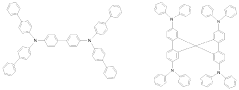
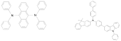
Key Patents and Innovations in OLED Printing Technology
Printing method for an organic light emitting diode (OLED)
PatentWO2018178136A1
Innovation
- A method using a piezo-printing device with an ink viscosity lower than 5 cP, adjusted to form two or more droplets of essentially the same size by controlling the actuation waveform, ensuring that the separated droplets are uniformly sized to improve resolution and prevent overspill into neighboring pixels.
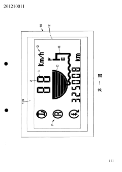
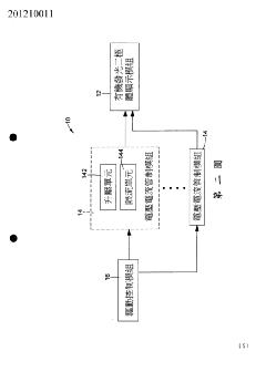
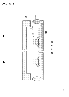
Icon organic light emitting diode display with high uniformity and brightness
PatentInactiveTW201210011A
Innovation
- A fixed-pattern OLED display with customized light-emitting diode elements of varying shapes, driven by DC power, utilizing voltage and current control modules to optimize power output and protect against damage, and incorporating a concave substrate for protection and moisture resistance.
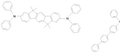
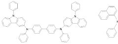
Material Science Advancements for OLED Printing
Recent advancements in material science have significantly contributed to improving OLED printing methods for achieving uniform brightness. The development of novel emissive materials with enhanced quantum efficiency has been a critical breakthrough, allowing for more consistent light emission across the entire display panel. Phosphorescent and thermally activated delayed fluorescence (TADF) materials have emerged as promising alternatives to traditional fluorescent compounds, offering higher energy conversion efficiency and more stable luminance properties.
Polymer chemistry innovations have led to the creation of solution-processable OLED materials with improved rheological characteristics, enabling more precise deposition during printing processes. These materials demonstrate better flow behavior and surface tension properties, resulting in more uniform thin films after deposition and drying. Cross-linkable polymers that can form stable networks after deposition have shown particular promise in preventing material redistribution during subsequent processing steps.
Host-dopant systems have been refined to ensure more homogeneous distribution of emissive molecules within the host matrix. Advanced co-solvent systems and solubility-enhancing additives have been developed to prevent phase separation and aggregation during the drying process, which previously led to brightness variations across printed areas. These formulations maintain consistent dopant concentration throughout the printed film, eliminating brightness hotspots.
Nanostructured materials and quantum dots have been incorporated into OLED formulations to provide more controlled and uniform emission characteristics. These materials offer narrow emission spectra and can be precisely tuned through size control during synthesis. Additionally, their surface chemistry can be modified to improve compatibility with printing processes, enhancing dispersion stability in printing inks.
Encapsulation materials have also evolved significantly, with new barrier films and hybrid organic-inorganic materials providing superior protection against moisture and oxygen. These advanced encapsulation solutions maintain the integrity of the printed OLED materials over longer periods, preventing degradation patterns that would otherwise lead to non-uniform brightness aging across the display.
Self-healing materials represent another frontier in OLED material science, with compounds capable of restructuring at the molecular level after thermal or electrical stress. These materials help maintain uniform electrical characteristics throughout the operational lifetime of the device, preventing the formation of high-resistance pathways that could cause brightness variations.
Environmental Impact and Sustainability of OLED Manufacturing
The environmental impact of OLED manufacturing processes, particularly printing methods, represents a critical consideration in the industry's sustainable development. Traditional OLED production techniques involve significant resource consumption and generate substantial waste, including hazardous chemicals and rare materials. The optimization of OLED printing methods for uniform brightness presents an opportunity to simultaneously address environmental concerns while improving product performance.
Current OLED manufacturing processes typically utilize vacuum thermal evaporation techniques that require considerable energy input and generate significant carbon emissions. The shift toward solution-based printing methods offers promising environmental benefits, including reduced energy consumption by approximately 30-40% compared to conventional techniques. These printing approaches operate at lower temperatures and eliminate the need for energy-intensive vacuum systems.
Material efficiency represents another significant environmental advantage of optimized OLED printing methods. Traditional manufacturing processes waste approximately 70-90% of organic materials during deposition, whereas advanced printing techniques can achieve material utilization rates exceeding 90%. This dramatic improvement reduces the demand for rare earth elements and other scarce resources while minimizing hazardous waste generation.
Water consumption in OLED manufacturing presents a substantial environmental challenge, with conventional processes requiring up to 1,500 liters per square meter of display produced. Optimized printing methods can reduce water requirements by 40-60% through more efficient deposition processes and reduced cleaning needs. This conservation becomes increasingly important as water scarcity affects manufacturing regions globally.
Chemical usage and toxicity reduction represent additional environmental benefits of advanced OLED printing techniques. By transitioning to water-based or less toxic solvents in printing formulations, manufacturers can significantly reduce volatile organic compound (VOC) emissions and worker exposure to hazardous substances. Several leading manufacturers have already achieved 50-70% reductions in hazardous chemical usage through printing optimization.
End-of-life considerations also favor optimized OLED printing methods. Displays manufactured with more uniform materials and fewer chemical additives typically offer improved recyclability. Research indicates that next-generation printed OLEDs could achieve recyclability rates of 80-85%, compared to current rates of approximately 20-30% for conventional displays.
The industry is increasingly adopting circular economy principles in OLED manufacturing, with several major producers implementing closed-loop systems for solvent recovery and material reclamation. These approaches, combined with optimized printing methods, can reduce the overall environmental footprint of OLED production by 40-60% according to recent life cycle assessments.
Unlock deeper insights with Patsnap Eureka Quick Research — get a full tech report to explore trends and direct your research. Try now!
Generate Your Research Report Instantly with AI Agent
Supercharge your innovation with Patsnap Eureka AI Agent Platform!