DDR5 vs DDR3: Signal Integrity Assessment
SEP 17, 20259 MIN READ
Generate Your Research Report Instantly with AI Agent
Patsnap Eureka helps you evaluate technical feasibility & market potential.
DDR Memory Evolution and Objectives
Dynamic Random Access Memory (DRAM) technology has undergone significant evolution since its inception in the late 1960s. The transition from DDR3 to DDR5 represents one of the most substantial leaps in memory technology, particularly in terms of signal integrity management. The development trajectory of DDR memory has been characterized by continuous improvements in bandwidth, capacity, and power efficiency to meet the escalating demands of computing systems.
DDR3, introduced in 2007, represented a significant advancement over its predecessors with operating frequencies ranging from 800 MHz to 2133 MHz. It featured a 64-bit data bus and employed fly-by topology for command and address signals, which helped mitigate signal integrity issues at higher speeds. However, as data rates increased, signal integrity challenges such as crosstalk, reflections, and jitter became increasingly problematic.
The intermediate DDR4 standard, launched in 2014, addressed some of these challenges through improved signal integrity features including pseudo-open drain (POD) I/O, data bus inversion (DBI), and enhanced termination schemes. These innovations laid the groundwork for the more radical changes implemented in DDR5.
DDR5, officially released in 2020, represents a paradigm shift in memory architecture with fundamental changes designed to overcome the signal integrity limitations of previous generations. Operating at frequencies from 4800 MHz to potentially 8400 MHz, DDR5 introduces decision feedback equalization (DFE), improved on-die termination, and a revolutionary dual-channel architecture that effectively splits each DIMM into two independent channels.
The primary objective of DDR memory evolution has been to balance the competing demands of increased bandwidth, reduced latency, enhanced capacity, and improved power efficiency while maintaining signal integrity at progressively higher frequencies. This balancing act has driven innovations in both memory chip design and system-level architecture.
Signal integrity assessment between DDR3 and DDR5 reveals the technological leap required to maintain reliable data transmission as speeds have increased more than fourfold. DDR5's architectural changes fundamentally alter the signal integrity landscape by reducing the electrical loading per channel, implementing more sophisticated equalization techniques, and providing better isolation between different signal paths.
The evolution trajectory aims to support emerging computational workloads including artificial intelligence, big data analytics, and high-performance computing applications that demand unprecedented memory bandwidth and capacity. Understanding this evolutionary path provides critical context for evaluating the signal integrity challenges and solutions that differentiate DDR3 and DDR5 technologies.
Market Demand Analysis for High-Speed Memory
The global memory market is experiencing a significant shift towards high-speed memory solutions, driven primarily by the exponential growth in data processing requirements across multiple sectors. The demand for DDR5 memory, which offers substantial improvements in signal integrity compared to DDR3, is projected to grow at a compound annual rate of 32% through 2027, reflecting the urgent need for higher bandwidth and improved power efficiency in modern computing systems.
Data centers represent the largest market segment for high-speed memory adoption, accounting for approximately 38% of the total demand. This is attributed to the proliferation of cloud computing services, big data analytics, and artificial intelligence applications that require massive parallel processing capabilities. Enterprise servers utilizing DDR5 memory can achieve up to 50% higher data throughput while maintaining superior signal integrity at higher frequencies compared to DDR3 implementations.
The consumer electronics sector follows closely, with gaming PCs, high-performance laptops, and next-generation gaming consoles driving the transition to DDR5. Market research indicates that premium gaming systems with DDR5 memory command a 15-20% price premium, demonstrating consumers' willingness to pay for enhanced performance. The improved signal integrity of DDR5 directly translates to more stable operation at higher clock speeds, which is particularly valuable in graphics-intensive applications.
Telecommunications infrastructure represents another critical growth area, particularly with the ongoing global deployment of 5G networks. Base stations and network routing equipment require memory solutions that can maintain signal integrity under demanding conditions while processing enormous data volumes. DDR5's advanced signal integrity features, including decision feedback equalization and improved voltage regulation, make it particularly suitable for these applications.
Industrial automation and automotive sectors are emerging as significant consumers of high-speed memory, driven by Industry 4.0 initiatives and the increasing computational requirements of advanced driver-assistance systems (ADAS). The automotive memory market specifically is expected to grow by 28% annually through 2026, with signal integrity being a critical factor in ensuring reliable operation in harsh environmental conditions.
Regional analysis reveals that Asia-Pacific dominates the high-speed memory market with 45% share, followed by North America at 30% and Europe at 20%. China's ambitious semiconductor self-sufficiency goals have accelerated domestic DDR5 production capabilities, while South Korea maintains leadership in advanced memory manufacturing technologies focused on signal integrity optimization.
Signal Integrity Challenges in DDR5 vs DDR3
Signal integrity challenges in DDR5 memory systems represent a significant evolution compared to DDR3, primarily due to the substantial increase in data rates. While DDR3 typically operates at 800-2133 MT/s, DDR5 pushes boundaries with speeds of 4800-8400 MT/s. This dramatic speed increase introduces more complex signal integrity issues that must be addressed through advanced design techniques.
The higher frequencies in DDR5 exacerbate transmission line effects, with impedance discontinuities becoming more problematic as wavelengths approach trace dimensions. Signal reflections that were manageable in DDR3 designs can cause severe data corruption in DDR5 systems. Additionally, the reduced voltage swing in DDR5 (1.1V compared to DDR3's 1.5V) creates a smaller noise margin, making systems more susceptible to signal degradation.
Crosstalk emerges as a critical challenge in DDR5 implementations. The combination of faster edge rates and denser routing creates stronger electromagnetic coupling between adjacent traces. This phenomenon is particularly problematic in the complex routing environments of modern motherboards and memory modules, where maintaining signal isolation becomes increasingly difficult.
DDR5 introduces decision feedback equalization (DFE) and feed-forward equalization (FFE) to compensate for channel losses at higher frequencies. These techniques, largely unnecessary in DDR3 designs, require sophisticated calibration procedures and add complexity to both design and testing processes. The equalization circuits must be carefully tuned to match specific channel characteristics.
Power integrity concerns are significantly heightened in DDR5 systems. The on-DIMM voltage regulation modules (VRMs) in DDR5 represent a fundamental architecture change from DDR3's motherboard-based power delivery. While this approach reduces noise on power rails, it introduces thermal management challenges and requires more sophisticated power integrity analysis during the design phase.
Timing margins have become exceedingly tight in DDR5 systems. With bit periods reduced to approximately 238 picoseconds at 4800 MT/s (compared to 938 picoseconds for DDR3-2133), the timing budget for setup and hold times, jitter, and skew has shrunk dramatically. This necessitates more precise timing analysis and potentially more complex clock distribution networks.
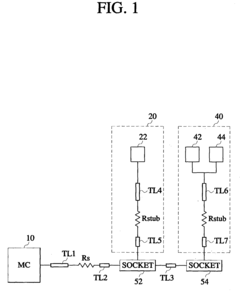
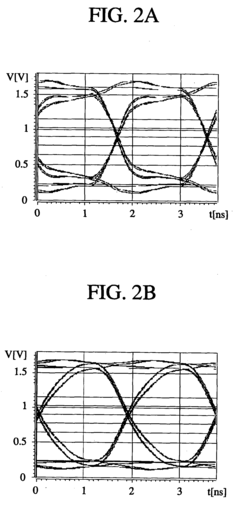
The testing and validation methodologies for DDR5 signal integrity require significant upgrades from DDR3 approaches. Higher bandwidth oscilloscopes, more sophisticated probing techniques, and advanced simulation tools are essential for accurately characterizing the high-speed signals. Eye diagram measurements must account for equalization effects, and compliance testing becomes more rigorous with tighter specifications.
The higher frequencies in DDR5 exacerbate transmission line effects, with impedance discontinuities becoming more problematic as wavelengths approach trace dimensions. Signal reflections that were manageable in DDR3 designs can cause severe data corruption in DDR5 systems. Additionally, the reduced voltage swing in DDR5 (1.1V compared to DDR3's 1.5V) creates a smaller noise margin, making systems more susceptible to signal degradation.
Crosstalk emerges as a critical challenge in DDR5 implementations. The combination of faster edge rates and denser routing creates stronger electromagnetic coupling between adjacent traces. This phenomenon is particularly problematic in the complex routing environments of modern motherboards and memory modules, where maintaining signal isolation becomes increasingly difficult.
DDR5 introduces decision feedback equalization (DFE) and feed-forward equalization (FFE) to compensate for channel losses at higher frequencies. These techniques, largely unnecessary in DDR3 designs, require sophisticated calibration procedures and add complexity to both design and testing processes. The equalization circuits must be carefully tuned to match specific channel characteristics.
Power integrity concerns are significantly heightened in DDR5 systems. The on-DIMM voltage regulation modules (VRMs) in DDR5 represent a fundamental architecture change from DDR3's motherboard-based power delivery. While this approach reduces noise on power rails, it introduces thermal management challenges and requires more sophisticated power integrity analysis during the design phase.
Timing margins have become exceedingly tight in DDR5 systems. With bit periods reduced to approximately 238 picoseconds at 4800 MT/s (compared to 938 picoseconds for DDR3-2133), the timing budget for setup and hold times, jitter, and skew has shrunk dramatically. This necessitates more precise timing analysis and potentially more complex clock distribution networks.
The testing and validation methodologies for DDR5 signal integrity require significant upgrades from DDR3 approaches. Higher bandwidth oscilloscopes, more sophisticated probing techniques, and advanced simulation tools are essential for accurately characterizing the high-speed signals. Eye diagram measurements must account for equalization effects, and compliance testing becomes more rigorous with tighter specifications.
Current Signal Integrity Solutions for DDR5
01 Signal integrity enhancement techniques for DDR memory
Various techniques are employed to enhance signal integrity in DDR memory systems, including impedance matching, termination schemes, and signal conditioning. These techniques help minimize signal reflections, reduce noise, and maintain signal quality across high-speed data paths. Advanced signal integrity solutions address issues such as crosstalk, jitter, and signal degradation that become more pronounced at higher data rates in DDR5 compared to DDR3.- Signal integrity enhancement techniques for DDR memory: Various techniques are employed to enhance signal integrity in DDR memory systems, particularly for DDR3 and DDR5 technologies. These include improved termination schemes, impedance matching, and signal conditioning circuits that reduce signal reflections and noise. Advanced circuit designs help maintain signal quality at higher frequencies, ensuring reliable data transmission between memory modules and controllers.
- Memory interface architecture for signal integrity: Specialized memory interface architectures are designed to address signal integrity challenges in DDR3 and DDR5 systems. These architectures incorporate optimized trace routing, buffer placement, and reference voltage management to minimize crosstalk and maintain signal quality. The interface designs account for the increasing data rates of newer DDR technologies while ensuring backward compatibility where needed.
- Timing and synchronization solutions for DDR memory: Precise timing and synchronization mechanisms are critical for maintaining signal integrity in DDR memory systems. These solutions include advanced clock distribution networks, delay-locked loops (DLLs), and phase-locked loops (PLLs) that help align data with clock signals. Calibration techniques are also implemented to compensate for variations in signal propagation delays across different channels and components.
- Testing and validation methods for DDR signal integrity: Comprehensive testing and validation methodologies are developed to ensure signal integrity in DDR memory systems. These include eye diagram analysis, jitter measurement, and bit error rate testing that help identify and resolve signal integrity issues. Simulation tools and hardware validation platforms enable designers to verify memory system performance under various operating conditions before final implementation.
- Power delivery network design for DDR signal integrity: Optimized power delivery network designs are essential for maintaining signal integrity in DDR memory systems. These designs incorporate decoupling capacitors, voltage regulators, and power plane structures that minimize power supply noise and ground bounce. Advanced power management techniques help reduce electromagnetic interference that can degrade signal quality, particularly at the higher frequencies used in DDR5 technology.
02 Memory controller architecture for DDR signal management
Memory controllers implement specialized architectures to manage signal integrity challenges in DDR memory systems. These controllers incorporate features such as adaptive equalization, timing calibration, and voltage reference adjustment to optimize signal quality. The controller architecture differs between DDR3 and DDR5, with DDR5 controllers featuring more sophisticated signal integrity management capabilities to handle higher data rates and more complex signaling requirements.Expand Specific Solutions03 On-die termination and impedance matching for DDR memory
On-die termination (ODT) and impedance matching techniques are critical for maintaining signal integrity in DDR memory systems. These features help reduce signal reflections at the receiver end and ensure proper signal transmission. DDR5 implements more advanced ODT schemes compared to DDR3, including calibrated termination resistors and dynamic ODT adjustments, which significantly improve signal quality at higher frequencies and help maintain data integrity during high-speed operations.Expand Specific Solutions04 Clock and data recovery techniques for DDR memory
Clock and data recovery techniques are essential for maintaining synchronization and signal integrity in DDR memory systems. These include delay-locked loops (DLLs), phase-locked loops (PLLs), and timing calibration mechanisms that ensure proper alignment between clock and data signals. DDR5 implements more sophisticated clock recovery techniques than DDR3, including enhanced training sequences and adaptive timing adjustments, to maintain signal integrity at significantly higher data rates.Expand Specific Solutions05 Power integrity and voltage regulation for DDR signal quality
Power integrity and voltage regulation play crucial roles in maintaining signal integrity in DDR memory systems. Techniques such as decoupling capacitors, power distribution network optimization, and voltage reference generation help minimize power supply noise that can degrade signal quality. DDR5 introduces on-die voltage regulation modules (VRMs) unlike DDR3's motherboard-based regulation, providing more stable power delivery closer to the point of load, which significantly improves signal integrity at higher frequencies.Expand Specific Solutions
Key Memory Manufacturers and Ecosystem
The DDR5 vs DDR3 signal integrity landscape is evolving rapidly, with the market currently in a transition phase as DDR5 adoption accelerates. The global DRAM market, valued at approximately $90 billion, shows significant growth potential for DDR5 technology. From a technical maturity perspective, industry leaders like Samsung, SK Hynix, and Micron have established strong DDR5 portfolios with advanced signal integrity solutions addressing higher frequencies and stricter timing requirements. Companies including Intel, Qualcomm, and Huawei are integrating these technologies into their systems, while specialized players like Montage Technology and ChangXin Memory are developing complementary components. Hon Hai Precision and Renesas Electronics are focusing on manufacturing optimization to address the more complex signal integrity challenges in DDR5, which requires more sophisticated design approaches than DDR3's established technology.
Micron Technology, Inc.
Technical Solution: Micron's DDR5 signal integrity solution employs advanced on-die termination (ODT) techniques with decision feedback equalization (DFE) to maintain signal quality at higher speeds. Their approach includes implementing adaptive equalization that dynamically adjusts to channel conditions, significantly reducing inter-symbol interference at 4800-6400 MT/s speeds. Micron has developed proprietary Power Management Integrated Circuits (PMICs) on their DDR5 modules that improve voltage regulation directly on the DIMM, reducing noise and improving signal integrity compared to DDR3's motherboard-based power delivery. Their DDR5 design incorporates enhanced reflection management through optimized trace impedance matching and improved crosstalk isolation between adjacent signal lines, allowing for reliable operation at twice the data rates of DDR3 while maintaining signal integrity across longer traces.
Strengths: Superior signal integrity at high frequencies with reduced noise margins; on-DIMM power management reduces motherboard-level interference; advanced equalization techniques enable reliable operation at higher speeds. Weaknesses: Higher implementation complexity requiring more sophisticated PCB design; increased cost due to additional components like PMICs; higher power consumption for equalization circuits.
Samsung Electronics Co., Ltd.
Technical Solution: Samsung's DDR5 signal integrity solution features their High-K Metal Gate (HKMG) process technology that reduces current leakage and improves signal stability at higher frequencies. Their design implements a sophisticated Decision Feedback Equalizer (DFE) and Feed-Forward Equalizer (FFE) combination that pre-compensates for channel loss and reflections, maintaining signal integrity at speeds up to 7200 MT/s. Samsung has developed an innovative dual-channel architecture that effectively splits the memory module into two independent channels, reducing signal loading and improving signal integrity compared to DDR3's single-channel approach. Their DDR5 modules incorporate on-die ECC (Error Correction Code) that detects and corrects single-bit errors before they propagate through the system, significantly enhancing signal reliability compared to DDR3's system-level ECC implementation.
Strengths: HKMG process technology provides superior signal stability at high frequencies; dual-channel architecture reduces signal degradation; on-die ECC improves data reliability without system overhead. Weaknesses: Higher manufacturing complexity increases production costs; requires more sophisticated motherboard designs to fully utilize capabilities; higher power requirements for advanced signal processing features.
Critical Patents in DDR5 Signal Integrity
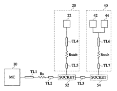
Memory signal transmission system, signal line arrangement method, product, equipment and medium
PatentActiveCN118711625A
Innovation
- By optimizing the length of the signal line and the length of the via in the inner layer of the circuit board, using the principle of matching short holes with long signal lines and long holes with short signal lines, a link model is established for crosstalk analysis and adjustment, and the signal lines are optimized. Arranged to reduce crosstalk values.
Memory system having memory modules with different memory device loads
PatentInactiveUS20040024966A1
Innovation
- The length of the signal transmission line of the SIMM is increased relative to the DIMM to compensate for the different loads, thereby reducing signal delay time differences and enhancing signal integrity.
Power Integrity Considerations for DDR5
Power integrity has emerged as a critical consideration in the transition from DDR3 to DDR5 memory technologies. DDR5 operates at significantly higher data rates (up to 6400 MT/s compared to DDR3's 2133 MT/s), necessitating stricter power delivery requirements to maintain system stability and performance.
The voltage regulation architecture represents one of the most fundamental changes in DDR5. Unlike DDR3, which relies on motherboard-based voltage regulation, DDR5 incorporates Power Management Integrated Circuits (PMICs) directly onto the memory modules. This on-DIMM voltage regulation reduces power delivery network (PDN) impedance and minimizes voltage droop during high-current transient events, addressing a key limitation in DDR3 systems.
DDR5 operates at a reduced core voltage of 1.1V compared to DDR3's 1.5V or 1.35V, resulting in approximately 20% lower power consumption. However, this voltage reduction narrows the noise margin, making DDR5 more susceptible to power integrity issues. The voltage tolerance in DDR5 has tightened to ±3% from DDR3's ±5%, requiring more precise power delivery systems.
The power delivery network for DDR5 must accommodate higher current demands despite lower operating voltages. Peak currents can reach 50-60A per module during intensive operations, compared to 15-20A in DDR3 systems. This necessitates more robust power planes, additional decoupling capacitors, and optimized PDN impedance profiles to maintain voltage stability across a wider frequency range.
Decoupling strategies have evolved significantly for DDR5. The technology employs a multi-tiered capacitor network, including on-die capacitance, on-package capacitors, and on-board bulk capacitors. This hierarchical approach addresses different frequency domains of power noise, from high-frequency switching noise to low-frequency load transients, providing superior noise suppression compared to DDR3's simpler decoupling schemes.
Thermal considerations have become increasingly important as DDR5 power density increases. Despite lower operating voltages, the higher operating frequencies generate more localized heating. Thermal sensors integrated into DDR5 modules enable real-time temperature monitoring and dynamic frequency adjustment to prevent thermal throttling, a capability largely absent in DDR3 systems.
Power-related signal integrity issues manifest differently in DDR5. Simultaneous switching noise (SSN) effects are more pronounced due to higher edge rates, requiring careful optimization of ground returns and power plane coupling. Advanced simulation techniques, including power-aware signal integrity analysis, have become essential for DDR5 designs to account for the complex interactions between power and signal domains.
PCB Design Requirements for DDR5 Implementation
The implementation of DDR5 memory interfaces demands significantly more stringent PCB design requirements compared to previous generations. The higher operating frequencies of DDR5 (4800-6400 MT/s initially, with roadmaps to 8400+ MT/s) necessitate meticulous attention to signal integrity considerations that were less critical for DDR3 designs.
PCB material selection becomes paramount for DDR5 implementation. Low-loss materials with controlled dielectric constants (Dk) and dissipation factors (Df) are essential to minimize signal degradation at multi-gigahertz frequencies. Materials such as Megtron 6 or similar with Df values below 0.005 are recommended, whereas DDR3 designs could often utilize standard FR-4 materials.
Transmission line design requires precise impedance control for DDR5, typically maintaining 40Ω single-ended and 80-85Ω differential impedances with tolerances of ±10% or better. This demands tighter manufacturing specifications and more sophisticated stackup designs with controlled prepreg and core thicknesses.
Layer count and stackup complexity increase substantially with DDR5. Minimum recommended stackups often require 8-10 layers with dedicated ground planes adjacent to signal layers carrying DDR5 traces. Power delivery network (PDN) design becomes more complex, requiring lower impedance across a broader frequency range to support the faster switching transients.
Trace routing guidelines for DDR5 are considerably more restrictive. Maximum trace lengths decrease to approximately 5-6 inches (compared to 8+ inches for DDR3), and length matching tolerances tighten to ±3 mils for address/command signals and ±1 mil for data groups. Serpentine patterns must be designed with careful consideration of coupling effects and return path discontinuities.
Via design and placement demand special attention in DDR5 implementations. Back-drilling becomes nearly mandatory to remove via stubs that create resonances at DDR5 frequencies. Via-to-trace transitions require careful modeling and optimization to minimize impedance discontinuities that were often negligible in DDR3 designs.
Ground plane continuity and return path management are critical for DDR5. Split planes must be avoided under DDR5 signals, and stitching vias must be strategically placed to maintain return current paths. Reference plane changes should be minimized, and when unavoidable, must be accompanied by sufficient stitching vias to maintain signal integrity.
Unlock deeper insights with Patsnap Eureka Quick Research — get a full tech report to explore trends and direct your research. Try now!
Generate Your Research Report Instantly with AI Agent
Supercharge your innovation with Patsnap Eureka AI Agent Platform!