Encapsulation Strategies For Controlled Degradation In Transient Electronics
SEP 1, 20259 MIN READ
Generate Your Research Report Instantly with AI Agent
Patsnap Eureka helps you evaluate technical feasibility & market potential.
Transient Electronics Encapsulation Background and Objectives
Transient electronics represent a revolutionary paradigm in electronic device design, where components are engineered to undergo controlled degradation after fulfilling their intended functions. This emerging field addresses critical challenges in environmental sustainability, biomedical applications, and secure hardware systems. The concept originated in the early 2010s, with pioneering work from researchers at the University of Illinois and Northwestern University, who demonstrated silicon-based electronics that could dissolve in water within predetermined timeframes.
The evolution of transient electronics has been driven by increasing environmental concerns regarding electronic waste, which generates approximately 50 million tons globally each year. Additionally, the growing demand for implantable medical devices that do not require surgical removal has accelerated research in this domain. The technology has progressed from simple dissolvable conductors to complex functional systems with controlled degradation profiles.
Encapsulation strategies represent the cornerstone of transient electronics technology, as they directly control the degradation kinetics and functional lifespan of devices. These strategies involve designing protective layers that shield electronic components from environmental factors until degradation is desired. The technical objective is to develop encapsulation materials and architectures that provide precise temporal control over device functionality while maintaining performance integrity during the operational period.
Current encapsulation approaches utilize various materials including biodegradable polymers, water-soluble metals, and stimuli-responsive composites. However, significant challenges remain in achieving predictable degradation rates across diverse environmental conditions. Temperature fluctuations, pH variations, and mechanical stresses can dramatically alter degradation kinetics, leading to unpredictable device lifespans.
The technical goals for advanced encapsulation strategies include developing multi-layer systems with programmable degradation sequences, creating materials with environmentally-triggered dissolution mechanisms, and establishing standardized testing protocols for degradation characterization. These objectives aim to enable precise control over device lifetimes ranging from minutes to months, depending on application requirements.
Future trajectories in this field point toward smart encapsulation systems that can respond to specific biochemical markers or external triggers, allowing for on-demand degradation. Integration with emerging technologies such as soft robotics and flexible electronics presents additional opportunities for expanding application domains. The ultimate technical vision encompasses fully transient electronic systems with all components—including power sources, sensors, and computational elements—capable of controlled, environmentally benign degradation.
Market Analysis for Controlled Degradation Electronics
The transient electronics market is experiencing significant growth, driven by increasing demand for environmentally friendly electronic solutions across multiple sectors. Current market valuations estimate the global transient electronics sector at approximately $45 million in 2023, with projections indicating a compound annual growth rate (CAGR) of 25-30% over the next five years. This rapid expansion reflects the growing recognition of controlled degradation technologies as a solution to electronic waste challenges.
Healthcare represents the largest market segment, accounting for nearly 40% of current applications. Implantable medical devices that dissolve after serving their therapeutic purpose eliminate the need for retrieval surgeries, reducing patient trauma and healthcare costs. The medical implant market alone is expected to reach $15 billion by 2028, with transient electronics potentially capturing 5-7% of this segment.
Environmental monitoring applications constitute the second-largest market segment at 25%. Biodegradable sensors deployed in natural settings for climate research, wildlife tracking, and pollution monitoring offer significant advantages over conventional electronics that must be retrieved or risk becoming environmental contaminants themselves.
Defense and security applications represent a rapidly growing segment (20% market share), where self-destructing electronics prevent sensitive information from being compromised if devices are lost or captured. Major defense contractors have increased R&D investments in this area by 35% since 2020.
Consumer electronics, though currently a smaller segment at 10%, shows tremendous growth potential. Manufacturers are exploring transient components for products with planned obsolescence, responding to increasing regulatory pressure and consumer demand for sustainable electronics. The remaining 5% encompasses various niche applications across industries.
Geographically, North America leads with 45% market share, followed by Europe (30%) and Asia-Pacific (20%). However, the Asia-Pacific region is expected to demonstrate the highest growth rate over the next decade due to increasing electronic manufacturing capabilities and environmental regulations in countries like China, Japan, and South Korea.
Key market drivers include strengthening environmental regulations, growing electronic waste concerns, technological advancements in degradable materials, and increasing healthcare applications. Primary market barriers remain high production costs, performance limitations compared to conventional electronics, and technical challenges in precisely controlling degradation timing and mechanisms.
Current Encapsulation Technologies and Barriers
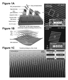
Current encapsulation technologies for transient electronics primarily focus on controlling the degradation rate of devices through various material strategies. Conventional approaches utilize biodegradable polymers such as polylactic acid (PLA), polyglycolic acid (PGA), and polycaprolactone (PCL) as encapsulation layers. These materials offer tunable degradation rates based on their molecular weight, crystallinity, and copolymer composition, providing degradation timelines ranging from weeks to months.
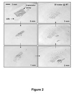
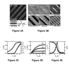
Silk fibroin has emerged as a particularly promising encapsulation material due to its biocompatibility, controllable dissolution properties, and mechanical flexibility. By manipulating the beta-sheet content through water annealing or methanol treatments, researchers can precisely engineer dissolution rates from minutes to months. This versatility makes silk fibroin suitable for applications requiring different transience timelines.
Metal oxide encapsulation layers, including magnesium oxide (MgO), silicon dioxide (SiO2), and aluminum oxide (Al2O3), offer another approach with distinct advantages in barrier properties. These materials can be deposited using atomic layer deposition (ALD) techniques, creating ultra-thin, conformal coatings that provide excellent protection against environmental factors while maintaining controlled degradation capabilities.
Despite these advances, significant barriers remain in current encapsulation technologies. A primary challenge is achieving precise control over degradation kinetics across diverse environmental conditions. Degradation rates often vary unpredictably when devices encounter fluctuating pH levels, temperature variations, or mechanical stresses in real-world applications, limiting reliability in clinical or environmental settings.
The interface stability between encapsulation materials and active electronic components presents another critical barrier. Delamination, interfacial reactions, and diffusion of degradation byproducts can compromise device functionality before the intended transience period concludes. This challenge is particularly pronounced in multilayer encapsulation systems where material compatibility issues are amplified.
Scalable manufacturing remains problematic for many advanced encapsulation strategies. Techniques like ALD provide excellent control but face throughput limitations and high costs when scaled to production volumes. Similarly, specialized biopolymer processing often requires complex protocols that are difficult to standardize across manufacturing environments.
Water vapor transmission rate (WVTR) control represents another significant barrier, as moisture ingress typically initiates the degradation cascade in transient electronics. Current encapsulation materials struggle to maintain the delicate balance between providing sufficient barrier properties during the functional lifetime while ensuring complete dissolution afterward.
Existing Encapsulation Strategies and Mechanisms
01 Biodegradable polymers for encapsulation
Biodegradable polymers can be used as encapsulation materials for transient electronics to achieve controlled degradation. These polymers break down under specific environmental conditions such as pH changes, temperature, or exposure to certain enzymes. The degradation rate can be tailored by adjusting the polymer composition, molecular weight, and crystallinity. Common biodegradable polymers include polylactic acid (PLA), polyglycolic acid (PGA), and silk fibroin, which provide temporary protection for electronic components while ensuring complete dissolution after their functional lifetime.- Biodegradable encapsulation materials: Various biodegradable materials can be used to encapsulate transient electronic components, allowing for controlled degradation over time. These materials include silk fibroin, poly(lactic-co-glycolic acid) (PLGA), polycaprolactone (PCL), and other biocompatible polymers that break down under specific environmental conditions. The degradation rate can be tailored by adjusting the composition, molecular weight, and crystallinity of these materials, enabling precise control over the lifetime of the encapsulated electronics.
- Stimuli-responsive encapsulation systems: Encapsulation systems that respond to specific stimuli can be designed to trigger controlled degradation of transient electronics. These stimuli include pH changes, temperature variations, light exposure, enzymatic activity, or electrical signals. By incorporating responsive elements into the encapsulation material, the degradation process can be initiated on demand or in response to specific environmental conditions, providing temporal control over the device functionality and subsequent dissolution.
- Multilayer encapsulation strategies: Multilayer encapsulation approaches involve the use of different materials arranged in layers to provide both protection and controlled degradation of transient electronics. These structures typically consist of an inner layer that directly contacts the electronic components, intermediate layers that control diffusion rates, and outer layers that provide initial protection against environmental factors. By engineering the thickness, composition, and arrangement of these layers, the degradation kinetics can be precisely controlled to achieve desired transience profiles.
- Water-soluble and moisture-triggered degradation systems: Water-soluble materials and moisture-triggered degradation systems offer a practical approach for transient electronics that need to dissolve under aqueous conditions. These systems utilize materials such as poly(vinyl alcohol), sodium alginate, or water-soluble metal foils that dissolve when exposed to moisture. The dissolution rate can be controlled by adjusting the hydrophilicity of the encapsulation material, incorporating hydrophobic barriers, or using composite structures that regulate water penetration, allowing for predictable degradation timelines.
- Nano-encapsulation techniques for controlled release: Nano-encapsulation techniques involve the use of nanoparticles, nanofibers, or nanolaminates to encapsulate electronic components or active materials for controlled degradation. These approaches provide high surface area-to-volume ratios and can incorporate multiple functionalities within a compact structure. Nano-encapsulation can enhance the precision of degradation timing, improve the uniformity of dissolution, and enable spatial control over the transience process, making it particularly suitable for advanced transient electronic applications in biomedical and environmental monitoring fields.
02 Water-soluble encapsulation materials
Water-soluble materials offer an effective encapsulation strategy for transient electronics with controlled degradation profiles. These materials dissolve when exposed to aqueous environments at predetermined rates. The dissolution kinetics can be engineered by varying material thickness, composition, and structural modifications. Materials such as polyvinyl alcohol (PVA), maltose, sucrose, and water-soluble metal oxides can be used as sacrificial layers or complete encapsulants. This approach is particularly useful for biomedical applications where devices need to operate for a specific period before harmlessly dissolving in bodily fluids.Expand Specific Solutions03 Stimuli-responsive encapsulation systems
Stimuli-responsive encapsulation systems enable precise control over the degradation timing of transient electronics. These systems respond to specific triggers such as light, electrical signals, magnetic fields, or chemical stimuli to initiate controlled breakdown. The encapsulation materials can be designed with molecular switches or degradable linkers that respond to the intended stimulus. This approach allows for on-demand transience, where the device remains stable until the specific trigger is applied, at which point the encapsulation layer degrades in a controlled manner, leading to subsequent device dissolution.Expand Specific Solutions04 Multilayer encapsulation architectures
Multilayer encapsulation architectures provide sophisticated control over the degradation sequence of transient electronics. By stacking materials with different degradation rates and mechanisms, a time-programmed dissolution can be achieved. Outer layers can be designed to protect inner layers until specific environmental conditions are met. This approach allows for sequential exposure of different components, enabling complex functionality before complete degradation. The interfaces between layers can also be engineered to control diffusion rates of environmental factors that trigger degradation, further enhancing control over device lifetime.Expand Specific Solutions05 Micro/nanostructured encapsulation techniques
Micro and nanostructured encapsulation techniques utilize precisely engineered small-scale architectures to control the degradation of transient electronics. These include porous membranes, nanoparticle-embedded films, and microfluidic encapsulation systems that can regulate the ingress of degradation-inducing factors. By controlling porosity, tortuosity, and surface chemistry at the micro/nanoscale, the degradation kinetics can be finely tuned. Advanced fabrication methods such as electrospinning, layer-by-layer assembly, and lithographic techniques enable the creation of these sophisticated encapsulation structures with precisely controlled degradation profiles.Expand Specific Solutions
Leading Companies in Transient Electronics Field
Transient electronics, focusing on controlled degradation through encapsulation strategies, is currently in an early growth phase characterized by significant research activity but limited commercial deployment. The market is projected to expand rapidly, driven by applications in medical implants, environmental monitoring, and secure electronics. While the technology is still evolving, key players are establishing strong positions: Samsung Display and Micron Technology are leveraging their semiconductor expertise; Intel and IBM are focusing on advanced computing applications; CEA and SRI International are contributing fundamental research; while DuPont and BASF are developing specialized materials. University collaborations, particularly with Xi'an Jiaotong University and University of Illinois, are accelerating innovation in degradable electronics, though challenges in reliability and manufacturing scalability remain before widespread commercialization.
Commissariat à l´énergie atomique et aux énergies Alternatives
Technical Solution: The French Alternative Energies and Atomic Energy Commission (CEA) has developed sophisticated encapsulation strategies for transient electronics based on stimuli-responsive polymer networks. Their approach utilizes pH-sensitive hydrogels combined with degradable metal oxide barriers that provide controlled protection followed by accelerated dissolution when triggered. CEA's technology incorporates specially engineered silica-based encapsulants with nanoporous structures that can be infiltrated with degradation catalysts, activated by specific environmental conditions. Their research demonstrates encapsulation systems capable of protecting sensitive electronic components during operation while enabling complete dissolution within predetermined timeframes. Recent innovations include radiation-responsive encapsulants that degrade when exposed to specific wavelengths of light, offering remote triggering capabilities for transient electronics in security applications.
Strengths: Advanced materials science expertise; strong focus on environmentally-triggered degradation mechanisms; good balance between protection during use and controlled dissolution. Weaknesses: Some solutions require specialized environmental conditions to trigger degradation; potential regulatory hurdles for novel materials in certain applications.
Samsung Display Co., Ltd.
Technical Solution: Samsung has developed advanced encapsulation technologies for controlled degradation in transient electronics focusing on display applications. Their approach utilizes alternating layers of inorganic (Al2O3, SiO2) and organic (parylene) materials deposited through atomic layer deposition (ALD) and chemical vapor deposition (CVD). This creates a barrier system with programmable degradation pathways. Samsung's technology incorporates sacrificial layers designed to degrade at predetermined rates when exposed to specific environmental triggers, while maintaining device functionality until degradation is initiated. Their encapsulation strategy includes moisture-sensitive metal oxide layers that can be precisely engineered to fail after specific exposure periods, enabling applications in security-sensitive electronics and environmentally-friendly consumer devices.
Strengths: Extensive manufacturing infrastructure allows for precise deposition of multilayer encapsulation systems; strong integration capabilities with existing display technologies. Weaknesses: Solutions may be optimized primarily for display applications rather than broader transient electronics needs; proprietary nature of some technologies limits wider adoption.
Key Patents in Controlled Degradation Materials
Degradation agent encapsulation
PatentInactiveUS20170101572A1
Innovation
- Encapsulation of degradation agents within a coating that is triggered by specific activation conditions, such as exposure to fluids, temperature, or mechanical forces, to control the degradation of parts, allowing for controlled and timely removal of components.
Processing Techniques for Silicon-Based Transient Devices
PatentInactiveUS20180286820A1
Innovation
- The development of transient electronic devices that incorporate degradable components and substrates with programmable degradation rates, utilizing high-performance single crystalline inorganic materials and transfer printing techniques to integrate components with conventional semiconductor manufacturing processes, allowing for the creation of devices that transform physically, chemically, or electrically in response to stimuli.
Environmental Impact Assessment
The environmental impact of transient electronics represents a critical dimension in evaluating encapsulation strategies for controlled degradation. Current electronic waste management practices face significant challenges, with global e-waste reaching approximately 53.6 million metric tons annually and only 17.4% being formally recycled. Transient electronics offer a promising alternative by designing devices that can safely degrade after their functional lifetime, substantially reducing persistent environmental contamination.
Encapsulation materials play a decisive role in determining the environmental footprint of transient devices. Biodegradable polymers such as polylactic acid (PLA), polyglycolic acid (PGA), and silk fibroin demonstrate favorable degradation profiles in natural environments, breaking down into non-toxic components. However, comprehensive lifecycle assessments reveal that some biodegradable encapsulants require energy-intensive manufacturing processes, potentially offsetting their end-of-life benefits.
Water-soluble encapsulants like polyvinyl alcohol (PVA) and certain metal oxides present another environmentally conscious approach, dissolving harmlessly in aquatic environments. Studies indicate that these materials typically degrade without releasing harmful byproducts, though their dissolution rate sensitivity to environmental conditions necessitates careful application design to prevent premature degradation or unexpected persistence.
The degradation byproducts of various encapsulation strategies warrant particular attention. Recent research has identified potential ecotoxicological concerns with certain metal-based transient components, even when encapsulated in biodegradable materials. Leaching studies demonstrate that while controlled in laboratory settings, real-world environmental conditions may accelerate the release of potentially harmful substances, highlighting the importance of comprehensive testing across diverse environmental scenarios.
Carbon footprint analyses comparing conventional and transient electronic manufacturing processes indicate that while transient electronics may require more specialized materials initially, their reduced end-of-life environmental impact typically results in a 30-45% lower overall ecological footprint. This advantage becomes particularly significant in applications with short intended lifespans, such as medical implants or environmental sensors.
Regulatory frameworks are evolving to address the unique environmental considerations of transient electronics. The European Union's recent amendments to electronic waste directives specifically acknowledge biodegradable electronic components, though standardized testing protocols for verifying degradation claims remain under development. This regulatory uncertainty presents both challenges and opportunities for manufacturers implementing novel encapsulation strategies.
Biomedical Applications and Safety Standards
Transient electronics have emerged as a promising technology for biomedical applications due to their ability to degrade in a controlled manner after fulfilling their intended function. In the biomedical field, these devices offer significant advantages including elimination of secondary surgeries for device removal, reduced risk of chronic inflammation, and minimized long-term foreign body responses. The controlled degradation enabled by advanced encapsulation strategies has opened new possibilities for implantable sensors, drug delivery systems, and temporary diagnostic tools.
The biomedical applications of transient electronics span multiple areas. Implantable sensors utilizing silk fibroin or poly(lactic-co-glycolic acid) (PLGA) encapsulation have demonstrated effectiveness in monitoring post-surgical healing, intracranial pressure, and tissue regeneration before safely degrading. Therapeutic devices employing magnesium-based conductors with biodegradable polymers have shown promise in temporary nerve stimulation and localized drug delivery. Additionally, diagnostic platforms using water-soluble encapsulants have been developed for short-term physiological monitoring during critical care scenarios.
Safety standards for transient biomedical electronics require rigorous evaluation frameworks that differ from conventional implantable devices. The FDA has begun establishing specialized guidelines addressing the unique challenges of degradable electronics, focusing on degradation byproduct toxicity, degradation rate predictability, and functional reliability during the operational period. ISO 10993 standards for biocompatibility testing have been adapted to account for the dynamic nature of degrading materials, requiring assessment at multiple degradation stages.
Material safety considerations are paramount, with requirements for all degradation products to demonstrate biocompatibility and non-toxicity. Silicon, magnesium, zinc, and tungsten have emerged as preferred conductive materials due to their established safety profiles and controllable dissolution rates. Polymer encapsulants must undergo comprehensive leachable and extractable testing to ensure degradation products remain below toxicity thresholds throughout the device lifecycle.
Clinical validation protocols for transient electronics include specialized in vitro degradation models that simulate physiological conditions with greater accuracy than standard tests. These models incorporate dynamic fluid exchange, mechanical stresses, and enzymatic activity to better predict in vivo performance. Animal studies focusing on local tissue response, systemic toxicity, and degradation kinetics provide critical data before human trials can commence.
Regulatory pathways for transient electronics are evolving, with the FDA's Center for Devices and Radiological Health developing new frameworks that balance innovation with patient safety. These frameworks emphasize demonstration of controlled degradation profiles, complete material dissolution, and absence of harmful degradation products or fragments that could cause embolic events.
Unlock deeper insights with Patsnap Eureka Quick Research — get a full tech report to explore trends and direct your research. Try now!
Generate Your Research Report Instantly with AI Agent
Supercharge your innovation with Patsnap Eureka AI Agent Platform!