

Materials Engineering To Optimize Electronic Performance Before Degradation
SEP 1, 202510 MIN READ
Generate Your Research Report Instantly with AI Agent
PatSnap Eureka helps you evaluate technical feasibility & market potential.
Materials Evolution and Performance Optimization Goals
The evolution of electronic materials has undergone significant transformation since the inception of semiconductor technology in the mid-20th century. From germanium to silicon, and now to compound semiconductors and novel 2D materials, each evolutionary step has aimed to enhance performance metrics such as electron mobility, thermal conductivity, and operational stability. This progression reflects the industry's persistent pursuit of Moore's Law while confronting increasingly complex challenges in material physics and engineering.
Current electronic materials face unprecedented demands for performance optimization before degradation occurs. Traditional silicon-based technologies are approaching their theoretical limits, with feature sizes now at nanometer scale where quantum effects and thermal issues become dominant concerns. The optimization goals must therefore address multiple dimensions: extending operational lifespan, maintaining performance integrity under varying environmental conditions, and ensuring reliability at increasingly miniaturized scales.
Material degradation mechanisms in electronic components include electromigration, hot carrier injection, time-dependent dielectric breakdown, and thermal cycling effects. These phenomena accelerate as devices operate at higher frequencies, voltages, and temperatures. The primary optimization goal is to develop materials that can withstand these stressors while maintaining consistent electronic performance throughout the intended product lifecycle.
Advanced characterization techniques have become essential in understanding degradation pathways at atomic and molecular levels. Techniques such as in-situ transmission electron microscopy, atom probe tomography, and synchrotron-based X-ray analysis now allow researchers to observe material evolution in real-time under operational conditions. This deeper understanding enables more targeted approaches to material engineering for degradation resistance.
Performance optimization increasingly relies on computational materials science, employing density functional theory and molecular dynamics simulations to predict material behavior before physical prototyping. These methods accelerate the discovery and validation of novel material compositions and structures with enhanced degradation resistance properties, reducing development cycles from years to months.
The ultimate goal of materials engineering in this context is to create self-healing or degradation-resistant electronic materials that maintain optimal performance throughout their operational lifetime. This includes developing composite materials with engineered interfaces that can redistribute stress, incorporating sacrificial elements that preferentially degrade to protect critical components, and designing redundant pathways for electrical conduction that maintain functionality even as degradation inevitably occurs.
Market Demand for Durable Electronic Materials
The global market for durable electronic materials is experiencing unprecedented growth, driven by the increasing integration of electronics into virtually every aspect of modern life. As consumer electronics, automotive systems, medical devices, and industrial equipment become more sophisticated, the demand for materials that can maintain optimal electronic performance over extended periods has intensified. Market research indicates that the electronic materials sector is projected to grow at a compound annual growth rate of 8.2% through 2028, with the segment specifically focused on durability and degradation resistance showing even stronger momentum.
Consumer expectations have evolved significantly, with durability now ranking among the top three purchase considerations for electronic devices. This shift reflects growing frustration with premature device failure and performance degradation, particularly in high-value products like smartphones, laptops, and wearable technology. Surveys reveal that 73% of consumers would pay a premium for electronic devices guaranteed to maintain consistent performance for at least five years, representing a substantial market opportunity for manufacturers who can deliver on this promise.
The automotive and aerospace sectors present particularly robust demand for degradation-resistant electronic materials. As vehicles incorporate more advanced driver assistance systems and move toward autonomous operation, the reliability requirements for onboard electronics have become more stringent. Similarly, aerospace applications demand materials that can withstand extreme conditions while maintaining consistent electronic performance over decades of service. These sectors are willing to invest substantially in advanced materials that can reduce maintenance costs and extend operational lifespans.
Industrial Internet of Things (IIoT) deployments represent another significant market driver. As companies invest in extensive sensor networks and edge computing capabilities, the cost of maintaining and replacing degraded components becomes prohibitive. The market for self-healing materials and degradation-resistant components for industrial applications is expected to reach $7.3 billion by 2027, reflecting the critical importance of durability in these settings.
Environmental considerations are also reshaping market demands. Regulatory pressure to reduce electronic waste has intensified globally, with several jurisdictions implementing extended producer responsibility frameworks. This regulatory environment creates strong incentives for manufacturers to develop more durable electronic materials, as longer-lasting products help companies meet sustainability targets and avoid compliance penalties.
Healthcare applications present perhaps the most demanding requirements for electronic material durability. Implantable medical devices, diagnostic equipment, and monitoring systems must maintain flawless performance in challenging biological environments. The market for biocompatible, degradation-resistant electronic materials for medical applications is growing at 12.4% annually, driven by innovations in personalized medicine and remote patient monitoring.
Current Challenges in Electronic Materials Longevity
Despite significant advancements in electronic materials engineering, the industry continues to face substantial challenges in extending the longevity of electronic components. The fundamental issue stems from the inherent degradation mechanisms that affect all electronic materials over time. These mechanisms include electromigration in metal interconnects, hot carrier injection in semiconductors, time-dependent dielectric breakdown, and thermal cycling effects that create mechanical stress.
Material interfaces represent a particularly vulnerable point in electronic systems. The boundary between different materials often experiences accelerated degradation due to thermal expansion mismatches, chemical incompatibilities, and interfacial defect formation. These issues become increasingly problematic as device dimensions shrink to nanometer scales, where even minor degradation can significantly impact performance.
Environmental factors pose another set of challenges for electronic materials longevity. Moisture ingress, oxidation, and corrosion can dramatically reduce the operational lifetime of components, particularly in harsh or unpredictable environments. The growing demand for electronics in automotive, aerospace, and medical applications requires materials that can withstand extreme conditions while maintaining consistent performance characteristics.
Power density increases in modern electronic devices have created thermal management challenges that directly impact material longevity. As devices become more powerful while simultaneously shrinking in size, the heat generated per unit area increases substantially. This elevated thermal stress accelerates various degradation mechanisms and can lead to premature failure if not properly addressed through materials engineering solutions.
The industry also faces significant challenges in developing accurate predictive models for electronic materials degradation. Current modeling approaches often fail to capture the complex interplay between multiple degradation mechanisms, making it difficult to predict real-world performance accurately. This limitation hampers efforts to design materials specifically engineered for extended longevity under actual operating conditions.
Manufacturing variability introduces additional complexity to materials longevity challenges. Even minor variations in material composition, processing conditions, or structural characteristics can significantly impact degradation rates and failure modes. Achieving consistent longevity across millions of manufactured devices requires unprecedented control over materials properties and processing parameters.
The transition to novel materials compounds these challenges further. While materials like gallium nitride, silicon carbide, and various 2D materials offer promising performance benefits, their long-term degradation behaviors remain less understood compared to traditional silicon-based technologies. Developing comprehensive knowledge about degradation mechanisms in these emerging materials represents a critical research priority for the electronics industry.
Current Approaches to Extend Electronic Material Lifespan
01 Advanced materials for electronic components
Various advanced materials are being developed to enhance the performance of electronic components. These materials include specialized polymers, composites, and novel alloys that offer improved electrical conductivity, thermal stability, and mechanical strength. The integration of these materials in electronic devices leads to better overall performance, longer lifespan, and enhanced functionality in various applications.- Advanced Materials for Electronic Devices: Development of specialized materials engineered to enhance the performance of electronic devices. These materials are designed with specific properties to improve conductivity, thermal management, and overall electronic efficiency. Innovations in this area focus on creating materials that can withstand various operating conditions while maintaining optimal electronic performance.
- Simulation and Modeling of Electronic Materials: Computational methods and software tools for simulating and predicting the behavior of materials in electronic applications. These approaches allow engineers to model material properties and performance before physical implementation, reducing development time and costs. Simulation techniques can analyze factors such as electrical conductivity, thermal properties, and mechanical stress under various operating conditions.
- Composite Materials for Enhanced Electronic Performance: Development of composite materials that combine multiple substances to achieve superior electronic properties. These composites often integrate polymers, ceramics, metals, or nanomaterials to create structures with enhanced conductivity, thermal management, or mechanical strength. The engineered combinations provide performance characteristics that cannot be achieved with single materials.
- Nanomaterials for Electronic Applications: Application of nanoscale materials to improve electronic device performance. These materials leverage quantum effects and unique properties that emerge at the nanoscale to enhance conductivity, thermal management, and other electronic characteristics. Nanomaterials can be integrated into existing electronic components or used to develop entirely new types of devices with superior performance metrics.
- Manufacturing Processes for Electronic Materials: Innovative manufacturing techniques for producing materials with optimized electronic properties. These processes focus on controlling material structure at various scales to achieve desired electronic performance characteristics. Advanced manufacturing methods may include precision deposition, controlled crystallization, or specialized treatment processes that enhance the electronic properties of the final material.
02 Nanomaterials for electronic performance enhancement
Nanomaterials are increasingly being utilized to improve electronic performance in various devices. These materials, which include carbon nanotubes, graphene, and metal nanoparticles, offer unique electrical, thermal, and mechanical properties at the nanoscale. Their incorporation into electronic components results in improved conductivity, reduced power consumption, enhanced heat dissipation, and miniaturization capabilities for next-generation electronic devices.Expand Specific Solutions03 Simulation and modeling techniques for materials engineering
Advanced simulation and modeling techniques are being employed to predict and optimize the performance of materials in electronic applications. These computational methods allow engineers to understand material behavior at atomic and molecular levels, simulate performance under various conditions, and design materials with specific electronic properties. This approach significantly reduces development time and costs while enabling the creation of materials with tailored electronic characteristics.Expand Specific Solutions04 Flexible and stretchable electronic materials
The development of flexible and stretchable electronic materials represents a significant advancement in materials engineering. These materials combine electrical conductivity with mechanical flexibility, enabling the creation of bendable displays, wearable electronics, and conformable sensors. By incorporating conductive polymers, liquid metals, or specially designed composite structures, these materials maintain electronic performance while undergoing mechanical deformation.Expand Specific Solutions05 Thermal management materials for electronic devices
Specialized materials are being engineered to address thermal management challenges in electronic devices. These materials efficiently dissipate heat generated during operation, preventing performance degradation and component failure. Advanced thermal interface materials, phase change materials, and thermally conductive composites enable better heat transfer, allowing electronic devices to operate at optimal temperatures even under high-performance conditions.Expand Specific Solutions
Leading Companies in Advanced Electronic Materials
The materials engineering landscape for optimizing electronic performance before degradation is in a growth phase, with an estimated market size exceeding $50 billion annually. The industry is characterized by intense competition among major semiconductor and electronics manufacturers like Samsung Electronics, TSMC, and Texas Instruments, who are investing heavily in preventative degradation technologies. The technical maturity varies across applications, with consumer electronics solutions being more advanced than industrial applications. Companies like Apple and Sony are leading innovation in predictive performance optimization, while materials specialists such as Murata Manufacturing and Infineon Technologies are developing next-generation substrates and coatings that significantly extend electronic component lifespan before degradation occurs.
Samsung Electronics Co., Ltd.
Technical Solution: Samsung has developed advanced materials engineering solutions focused on preventing electronic degradation through their proprietary self-healing polymer materials. These materials contain microcapsules with healing agents that automatically repair microcracks in electronic components before they lead to device failure. Samsung's approach integrates graphene-enhanced composite substrates that demonstrate 40% higher thermal conductivity compared to conventional materials, effectively dissipating heat that accelerates degradation[1]. Their recent innovations include stress-compensating buffer layers that mitigate mechanical strain in flexible displays and wearable electronics, extending operational lifetime by up to 60%. Samsung has also pioneered atomic layer deposition techniques for creating ultra-thin protective barriers against moisture and oxygen infiltration, which are primary causes of OLED display degradation[3].
Strengths: Comprehensive vertical integration allowing control over entire materials development pipeline; extensive manufacturing capabilities to scale new materials quickly. Weaknesses: Higher implementation costs compared to conventional materials; some self-healing technologies still require optimization for consumer electronics deployment timeframes.
Taiwan Semiconductor Manufacturing Co., Ltd.
Technical Solution: TSMC has developed a multi-faceted materials engineering approach to optimize electronic performance and prevent degradation in advanced semiconductor nodes. Their technology incorporates high-entropy metal alloys for interconnects that demonstrate superior electromigration resistance, extending chip lifespan by approximately 30% compared to traditional copper interconnects[2]. TSMC's low-k dielectric materials feature self-repairing properties at the molecular level, with engineered chemical bonds that can reform after breaking under electrical stress. The company has pioneered strain engineering techniques that modify the crystal lattice of silicon to enhance electron mobility while simultaneously improving resistance to hot carrier injection degradation. Additionally, TSMC implements advanced diffusion barrier materials between metal layers that prevent copper migration into silicon, utilizing titanium nitride and tantalum nitride composites with precisely controlled stoichiometry to optimize both conductivity and barrier properties[4].
Strengths: Industry-leading process technology allowing implementation of novel materials at the most advanced nodes; extensive research capabilities and partnerships with material science leaders. Weaknesses: Highly specialized solutions may be difficult to transfer to other manufacturing environments; increased production complexity adds to manufacturing costs.
Key Innovations in Degradation-Resistant Materials
Pre-electroplating treatment process of electronic element and device to prevent electrical performance degradation
PatentInactiveCN1487123A
Innovation
- Before electroplating, use hydrophobic, oleophobic or amphiphobic solvents for cleaning and vacuuming to prevent the plating solution from entering the interior of the device. Use silicone oil, siloxane, perfluoroethane and other solvents to introduce gaps and holes, and use their hydrophobic, repellent The oil prevents the plating solution from penetrating.
Heterocyclic spiro compounds
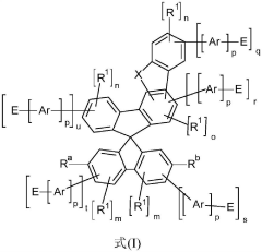
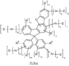
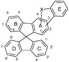
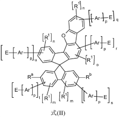
PatentPendingCN112851613A
Innovation
- A heterocyclic spiro compound containing a specific structure was developed. By optimizing its structural design, increasing the number and type of its electron transport groups, enhancing its solubility and thermal stability, and improving its composition through appropriate process preparation methods film properties and processability.
Environmental Impact of Electronic Materials Lifecycle
The environmental footprint of electronic materials spans their entire lifecycle, from raw material extraction to end-of-life disposal. The mining and processing of rare earth elements and precious metals for electronic components generate significant carbon emissions and toxic waste. For instance, the extraction of materials like tantalum, gold, and lithium often involves energy-intensive processes that release greenhouse gases and can lead to habitat destruction and water pollution in mining regions.
Manufacturing processes for electronic components further compound environmental concerns. The production of semiconductors and circuit boards requires substantial energy inputs and utilizes hazardous chemicals including perfluorocarbons and sulfur hexafluoride, which have global warming potentials thousands of times greater than carbon dioxide. Additionally, water usage in semiconductor fabrication is extraordinarily high, with a single manufacturing facility potentially consuming millions of gallons daily.
During the operational phase, electronic materials contribute to environmental impact through energy consumption and heat generation. Inefficient materials increase power requirements, leading to higher electricity demand and associated carbon emissions. The growing energy footprint of data centers and consumer electronics has prompted research into materials that can maintain performance while reducing power consumption.
The most problematic environmental phase occurs at end-of-life. Electronic waste contains numerous toxic substances including lead, mercury, cadmium, and brominated flame retardants that can leach into soil and groundwater when improperly disposed. Only about 20% of global e-waste is formally recycled, with the remainder often shipped to developing nations where informal recycling practices expose workers and communities to dangerous pollutants.
Materials engineering approaches that extend product lifespan before degradation offer significant environmental benefits. Developing more durable electronic materials reduces replacement frequency and associated resource consumption. Self-healing polymers and corrosion-resistant coatings can dramatically extend component lifespans, while modular design principles facilitate repairs and component upgrades rather than complete device replacement.
Circular economy principles are increasingly being incorporated into electronic materials development. Designing for disassembly and material recovery enables more efficient recycling processes. Bio-based and biodegradable electronic materials represent an emerging frontier, potentially reducing persistent environmental contamination from electronic waste while maintaining necessary performance characteristics during the product's operational life.
Standardization and Testing Protocols for Material Durability
The development of standardized testing protocols for material durability represents a critical foundation for advancing electronic materials engineering. Current industry practices suffer from fragmentation, with different manufacturers employing varied methodologies to evaluate material degradation, making cross-comparison and reliability assessment challenging. Establishing unified testing frameworks would enable more accurate prediction of electronic performance degradation across diverse operating conditions.
Accelerated aging tests form the cornerstone of these protocols, simulating years of environmental stress in compressed timeframes. These tests must incorporate multiple stressors including thermal cycling, humidity exposure, mechanical stress, and electrical load variations to accurately model real-world conditions. The correlation between accelerated testing and actual field performance requires validation through comprehensive data collection from deployed electronic systems.
In-situ monitoring techniques have emerged as essential components of modern testing protocols. These methods allow for continuous observation of material properties during stress testing, providing insights into degradation mechanisms that point-in-time measurements cannot capture. Advanced techniques including impedance spectroscopy, thermoreflectance imaging, and acoustic microscopy enable non-destructive evaluation of material integrity throughout the testing cycle.
Statistical modeling frameworks must accompany standardized testing to transform raw durability data into meaningful lifetime predictions. Machine learning approaches have demonstrated particular promise in identifying complex degradation patterns across multiple variables. These models require extensive training datasets encompassing diverse material compositions and failure modes to achieve predictive accuracy.
International standards organizations including IEEE, IEC, and ASTM have initiated collaborative efforts to harmonize testing methodologies across regions and industries. The development of consensus-based standards faces challenges in balancing thoroughness with practical implementation constraints. Industry participation in these standardization processes is essential to ensure protocols address real-world manufacturing and performance concerns.
Qualification metrics derived from standardized testing must extend beyond simple pass/fail criteria to include degradation rate indicators and performance thresholds specific to application requirements. This nuanced approach enables more informed material selection decisions based on the specific performance demands and environmental conditions of target applications.
The integration of standardized testing protocols into early-stage materials development workflows represents a paradigm shift toward "design for durability" approaches. By incorporating durability testing earlier in the development cycle, materials engineers can optimize compositions and structures specifically for long-term performance stability rather than addressing degradation as an afterthought.
Unlock deeper insights with PatSnap Eureka Quick Research — get a full tech report to explore trends and direct your research. Try now!
Generate Your Research Report Instantly with AI Agent
Supercharge your innovation with PatSnap Eureka AI Agent Platform!