

Solvent Processing Versus Vapor Deposition For Transient Device Layers
SEP 1, 20259 MIN READ
Generate Your Research Report Instantly with AI Agent
PatSnap Eureka helps you evaluate technical feasibility & market potential.
Transient Device Layer Processing Background and Objectives
Transient electronics represent a revolutionary paradigm in device technology, designed to operate for a predetermined period before harmlessly degrading or dissolving. The processing methods for creating these temporary functional layers stand at a critical technological crossroads, with solvent processing and vapor deposition emerging as the two dominant approaches. This technological domain has evolved significantly over the past decade, transitioning from conceptual research to practical applications in medical implants, environmental sensors, and secure electronics.
The historical trajectory of transient device layer processing began with rudimentary biodegradable polymers in the early 2000s, primarily utilizing solution-based techniques. By 2010, researchers had demonstrated the first fully transient electronic circuits using water-soluble substrates. The field gained substantial momentum around 2015 when vapor deposition techniques were adapted specifically for transient electronics, enabling unprecedented control over layer thickness and composition at the nanoscale.
Current technological trends indicate a growing convergence of hybrid approaches that leverage the advantages of both solvent processing and vapor deposition. The industry is witnessing increased emphasis on environmentally benign processing methods that align with the inherent sustainability goals of transient electronics. Additionally, there is a clear shift toward scalable manufacturing techniques that can transition these devices from laboratory curiosities to mass-produced commercial products.
The primary objective of this technical investigation is to comprehensively evaluate the relative merits and limitations of solvent processing versus vapor deposition for transient device layers. Specifically, we aim to assess performance parameters including dissolution kinetics, functional stability during operational lifetime, processing complexity, scalability potential, and environmental impact. This evaluation will provide crucial insights for strategic decision-making regarding manufacturing investments and research direction.
Secondary objectives include identifying potential hybrid approaches that might overcome the limitations of either method independently, mapping the intellectual property landscape to identify strategic opportunities, and forecasting technological developments likely to impact processing methodologies within the next five years. We also seek to establish quantitative benchmarks for comparing different processing techniques across various application domains.
The ultimate goal is to establish a technological roadmap that guides research and development efforts toward optimal processing solutions for next-generation transient electronics. This roadmap will consider not only technical performance metrics but also economic viability, regulatory compliance, and alignment with broader sustainability objectives that are increasingly driving innovation in this field.
Market Analysis for Dissolvable Electronics Applications
The dissolvable electronics market is experiencing significant growth, driven by increasing demand for environmentally friendly and biocompatible electronic devices. Current market projections indicate that the global transient electronics market is expected to reach $4.5 billion by 2026, with a compound annual growth rate of approximately 28% from 2021. This rapid expansion reflects the growing recognition of dissolvable electronics' potential across multiple industries.
Healthcare applications represent the largest market segment, accounting for nearly 45% of the total market share. Within this sector, implantable medical devices that naturally dissolve after serving their purpose are gaining substantial traction. These devices eliminate the need for secondary removal surgeries, reducing patient trauma and healthcare costs while minimizing infection risks.
Environmental monitoring constitutes another rapidly expanding application area, growing at 32% annually. Dissolvable sensors deployed in natural environments for data collection can completely degrade after use, leaving no electronic waste or environmental contamination. This aligns perfectly with increasing regulatory pressure and consumer demand for sustainable technology solutions.
Consumer electronics manufacturers are also exploring dissolvable components for temporary use products, particularly in wearable technology. This segment is projected to grow at 25% annually through 2026, with applications ranging from disposable health monitors to degradable components in conventional electronics.
The manufacturing methods for these dissolvable electronics—specifically solvent processing versus vapor deposition—significantly impact market adoption rates. Products manufactured using vapor deposition techniques currently command premium pricing due to their enhanced performance characteristics, though they represent only about 30% of the market due to higher production costs.
Regional analysis reveals North America leads the market with 38% share, followed by Europe at 29% and Asia-Pacific at 24%. However, the Asia-Pacific region demonstrates the fastest growth rate at 34% annually, driven by increasing manufacturing capabilities and rising healthcare expenditures.
Key market challenges include balancing dissolution rates with functional lifespans and scaling production processes while maintaining cost-effectiveness. The choice between solvent processing and vapor deposition directly influences these factors, with vapor deposition offering superior control over dissolution timing but at higher manufacturing costs.
Market forecasts suggest that as manufacturing technologies mature, particularly in vapor deposition methods, production costs will decrease by approximately 40% over the next five years, potentially accelerating market penetration across all application segments.
Current Challenges in Solvent and Vapor Deposition Technologies
Despite significant advancements in both solvent processing and vapor deposition technologies for transient device layers, several critical challenges persist that impede their widespread industrial adoption and optimization. Solvent processing methods, while cost-effective and scalable, continue to struggle with achieving uniform film morphology across large substrate areas. The inherent variability in solvent evaporation rates leads to inconsistent layer thickness and potential defect formation, particularly problematic for devices requiring precise dimensional control.
Material compatibility represents another significant hurdle for solvent-based approaches. Many advanced functional materials exhibit limited solubility in environmentally friendly solvents, forcing manufacturers to rely on toxic or hazardous alternatives that complicate manufacturing processes and increase regulatory compliance costs. Additionally, solvent-substrate interactions can trigger undesirable chemical reactions or structural modifications that compromise device performance.
Vapor deposition technologies face their own set of challenges, primarily centered around equipment complexity and operational costs. High-vacuum systems require substantial capital investment and specialized maintenance protocols, creating barriers to entry for smaller manufacturers and research facilities. The energy-intensive nature of these processes also raises sustainability concerns in an increasingly carbon-conscious industrial landscape.
Precise control of deposition parameters remains technically demanding, particularly for multi-component materials where stoichiometric precision is critical. Minor variations in chamber conditions can significantly alter film properties, necessitating sophisticated real-time monitoring systems that further increase system complexity and cost.
Scalability presents a persistent challenge for vapor deposition techniques. While laboratory-scale demonstrations have shown exceptional results, translating these achievements to industrial production volumes often reveals unforeseen complications in maintaining film quality and process reliability. The trade-off between throughput and precision continues to limit commercial viability for certain applications.
Both technologies face common challenges in interface engineering between dissimilar materials. The formation of clean, defect-free interfaces is crucial for transient device performance, yet achieving this consistently remains problematic. Interfacial defects, diffusion, and unwanted reactions can compromise device functionality and longevity, particularly in applications requiring controlled degradation characteristics.
Emerging hybrid approaches that combine aspects of both methodologies show promise but introduce additional complexity in process integration and quality control. The optimization of these hybrid techniques requires sophisticated modeling and characterization capabilities that are still evolving within the research community.
Comparative Analysis of Solvent Processing vs. Vapor Deposition Techniques
01 Transient electronic devices and biodegradable components
Transient electronic devices are designed to operate for a predetermined period before degrading or dissolving. These devices incorporate biodegradable layers that can break down under specific environmental conditions. The technology enables applications in medical implants, environmental monitoring, and temporary electronics that disappear after their useful life, reducing electronic waste. The transient layers typically consist of water-soluble polymers or materials that degrade through hydrolysis or enzymatic processes.- Transient electronic devices and biodegradable layers: Transient electronic devices incorporate biodegradable or dissolvable layers that can disappear or degrade under specific environmental conditions. These devices are designed to function for a predetermined period before breaking down, making them useful for medical implants, environmental sensors, and temporary electronics. The transient layers typically consist of water-soluble polymers, silk fibroin, or other materials that dissolve when exposed to bodily fluids or environmental factors.
- Sensing and measurement applications using transient layers: Transient device layers are utilized in various sensing and measurement applications, including biosensors, environmental monitoring, and diagnostic tools. These layers can be designed to respond to specific analytes or conditions, providing temporary measurement capabilities before degrading. The technology enables the development of disposable sensors that leave minimal environmental footprint after their useful life, while maintaining high accuracy during their operational period.
- Protective and sacrificial layers in semiconductor manufacturing: In semiconductor manufacturing, transient layers serve as protective or sacrificial elements during fabrication processes. These temporary layers shield underlying structures during etching, deposition, or other processing steps and are subsequently removed. The approach allows for more precise control of device geometries and properties, enabling the creation of complex multilayer structures while preventing damage to critical components during manufacturing.
- Transient interface layers for electronic and optical applications: Transient interface layers are designed to temporarily modify the properties between different materials or components in electronic and optical devices. These layers can alter electrical conductivity, optical transmission, or adhesion characteristics for a limited time before changing state or disappearing. Applications include temporary optical filters, switchable electronic interfaces, and adaptive optical systems where properties need to change during operation or lifecycle phases.
- Environmental and geological monitoring with transient layers: Transient device layers are employed in environmental and geological monitoring systems to track changes in soil conditions, water quality, or subsurface characteristics. These layers can be designed to respond to specific environmental triggers, providing data before degrading naturally. The technology enables deployment in remote or inaccessible locations where device retrieval would be difficult, allowing for temporary monitoring without long-term environmental impact.
02 Sensing and measurement applications using transient layers
Transient device layers are utilized in various sensing and measurement applications. These layers can be designed to change their properties in response to specific stimuli, enabling detection and measurement of environmental parameters, biological markers, or physical quantities. The temporary nature of these layers allows for one-time use sensors or devices that can be deployed in hard-to-reach locations without requiring retrieval. Applications include fluid analysis, biomedical diagnostics, and environmental monitoring systems.Expand Specific Solutions03 Protective and sacrificial layers in semiconductor manufacturing
In semiconductor manufacturing, transient layers serve as protective or sacrificial elements during fabrication processes. These temporary layers shield underlying structures during etching, deposition, or other processing steps and are subsequently removed. The use of such layers enables more complex device architectures and improves manufacturing yields by preventing damage to critical components. Materials used include photoresists, oxide layers, and various polymers that can be selectively removed through chemical or physical processes.Expand Specific Solutions04 Transient layers in data storage and memory devices
Transient layers are employed in data storage and memory applications to create devices with controllable data retention periods. These layers can be designed to degrade or change properties over time, effectively erasing stored information after a predetermined period. This technology is particularly valuable for security applications, temporary data storage, and situations where information should automatically expire. The degradation mechanisms can be triggered by various factors including time, temperature, or specific external stimuli.Expand Specific Solutions05 Transient layers in energy and power management systems
Transient device layers play a crucial role in energy and power management systems, particularly in protecting against voltage spikes, power surges, and electromagnetic interference. These layers can absorb or redirect excess energy during transient events, preventing damage to sensitive components. Additionally, some transient layers are designed to change their electrical properties in response to operating conditions, enabling adaptive power management. Applications include automotive electronics, industrial equipment, and consumer devices operating in variable power environments.Expand Specific Solutions
Leading Companies and Research Institutions in Transient Electronics
The solvent processing versus vapor deposition market for transient device layers is currently in a growth phase, with increasing applications in semiconductor, display, and electronics industries. The market is expanding at a significant rate due to rising demand for advanced manufacturing techniques that offer precise control over thin film properties. Leading players include Applied Materials, Tokyo Electron, and Samsung Display, who have established strong technological capabilities in vapor deposition, while companies like DuPont and Toray Industries excel in solvent processing technologies. Emerging competitors such as NAURA Microelectronics and Advanced Micro Fabrication Equipment are gaining market share by offering cost-effective solutions. The technology landscape shows vapor deposition reaching higher maturity levels for high-performance applications, while solvent processing continues to evolve with advantages in cost-efficiency and scalability.
Applied Materials, Inc.
Technical Solution: Applied Materials has developed comprehensive technical solutions for both solvent processing and vapor deposition methods for transient device layers. Their solvent processing technology utilizes spin coating and inkjet printing techniques optimized for uniform deposition of solution-processed materials including organic semiconductors and dielectrics. For vapor deposition, they offer advanced Physical Vapor Deposition (PVD) and Chemical Vapor Deposition (CVD) systems specifically designed for transient electronics, featuring precise thickness control down to nanometer scale and multi-chamber configurations that allow sequential deposition without breaking vacuum. Their Endura® platform incorporates temperature-controlled deposition for heat-sensitive transient materials, while their ALD (Atomic Layer Deposition) technology enables conformal coating with atomic-level precision for ultra-thin transient layers with controlled dissolution rates.
Strengths: Industry-leading equipment precision with sub-nanometer thickness control; integrated multi-process platforms reducing contamination risks; advanced in-situ monitoring capabilities. Weaknesses: Higher capital equipment costs compared to simple solvent processing setups; complex systems require specialized technical expertise for operation and maintenance.
Micron Technology, Inc.
Technical Solution: Micron Technology has developed specialized technical approaches for transient device layers focusing on memory applications. Their solution combines both solvent processing and vapor deposition techniques in a hybrid manufacturing approach. For solvent processing, they've engineered proprietary solvent formulations that enable precise deposition of silicon-based and metal oxide materials that can be programmed to degrade at specific rates. Their vapor deposition technology utilizes modified atomic layer deposition (ALD) processes optimized for transient materials, allowing atomic-level control of film composition and thickness. Micron's approach incorporates water-soluble substrates combined with controlled-lifetime electronic materials to create memory devices that can completely dissolve in physiological or environmental fluids within predetermined timeframes, ranging from minutes to months depending on the application requirements.
Strengths: Exceptional control over dissolution kinetics through material engineering; specialized expertise in memory applications; ability to tune degradation timelines precisely. Weaknesses: Solutions primarily focused on memory applications rather than broader transient electronics; higher production costs compared to conventional non-transient alternatives.
Key Patents and Scientific Breakthroughs in Transient Layer Development
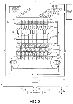
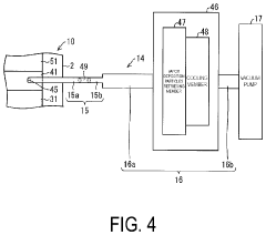
Method for vacuum processing of a substrate, thin film transistor, and apparatus for vacuum processing of a substrate
PatentWO2018145751A1
Innovation
- A method and apparatus that utilize particle implantation, where a substrate or material layer is irradiated with ions or neutral atoms using an implantation source while being moved through a processing region, allowing for the alteration of material properties like charge carrier mobility and threshold voltage, and potentially refractive index, to enhance the performance of thin film transistors.
Vapor deposition source and vapor deposition device for producing vapor deposition film with high material usage efficiency
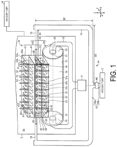
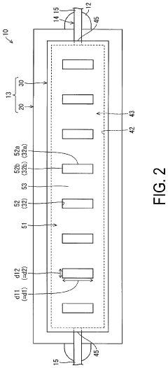
PatentActiveUS10760155B2
Innovation
- A vapor deposition source with multistage nozzle portions and a vacuum exhaust unit connected to spaces between the nozzles, adjusting pressure to ensure vapor deposition particles are emitted with higher directivity, reducing scattering and improving material usage efficiency.
Environmental Impact Assessment of Processing Methods
The environmental impact of manufacturing processes has become a critical consideration in the development of transient electronic devices. When comparing solvent processing and vapor deposition techniques for creating transient device layers, significant differences emerge in their ecological footprints, resource consumption, and waste generation profiles.
Solvent processing methods typically involve the use of organic solvents that may include toxic chemicals such as toluene, acetone, and chloroform. These substances pose potential environmental hazards through air emissions, water contamination, and soil pollution if not properly managed. The production, transportation, and disposal of these solvents contribute to the overall carbon footprint of the manufacturing process. Additionally, solvent recovery systems, while reducing waste, require substantial energy input, further increasing environmental impact.
Vapor deposition techniques, conversely, generally operate in vacuum environments and often eliminate the need for environmentally harmful solvents. However, these processes typically demand higher energy consumption due to the vacuum systems and high temperatures required. The energy-intensive nature of vapor deposition contributes significantly to greenhouse gas emissions when powered by non-renewable energy sources. Nevertheless, the absence of solvent waste represents a substantial environmental advantage.
Life cycle assessment (LCA) studies comparing these two approaches indicate that vapor deposition may offer reduced toxicity risks and lower waste management requirements, while solvent processing might present advantages in energy efficiency depending on the specific implementation. Recent research by Irimia-Vladu et al. (2020) demonstrated that optimized solvent processing using green solvents could reduce the carbon footprint by up to 40% compared to conventional vapor deposition for certain transient device applications.
Water consumption patterns also differ markedly between these techniques. Solvent processing typically requires significant water usage for cleaning and rinsing steps, whereas vapor deposition processes generally have minimal water requirements. This distinction becomes particularly relevant in regions facing water scarcity challenges.
Emerging hybrid approaches that combine elements of both methods show promise in minimizing environmental impact. For instance, atmospheric pressure vapor deposition techniques reduce energy requirements while maintaining the solvent-free advantages of traditional vacuum deposition. Similarly, aqueous-based solvent processing systems are being developed to eliminate the need for harmful organic solvents.
Regulatory frameworks increasingly influence processing method selection, with stricter environmental regulations in Europe and North America driving innovation toward greener manufacturing techniques. Companies adopting environmentally responsible processing methods may gain competitive advantages through regulatory compliance and enhanced brand reputation in environmentally conscious markets.
Scalability and Cost Efficiency Analysis
When comparing solvent processing and vapor deposition techniques for transient device layers, scalability and cost efficiency emerge as critical factors determining industrial adoption. Solvent processing methods, including spin coating, inkjet printing, and spray coating, demonstrate significant advantages in terms of capital expenditure. The equipment required for these processes typically costs between $10,000 and $100,000, substantially lower than vapor deposition systems that range from $500,000 to several million dollars.
Production throughput analysis reveals that solvent-based techniques can achieve higher processing speeds for large-area applications. Roll-to-roll manufacturing using solution processing can reach production rates of 10-100 m²/min, whereas typical vapor deposition systems operate at 1-10 m²/hour. This tenfold difference in throughput capacity directly impacts manufacturing economics, particularly for consumer electronics and disposable medical devices where cost sensitivity is paramount.
Material utilization efficiency presents another significant economic consideration. Solvent processing typically achieves 60-90% material utilization rates, while vapor deposition methods often operate at 10-40% efficiency due to overspray and chamber wall deposition. For expensive active materials, this difference translates to substantial cost savings in high-volume production scenarios.
Energy consumption metrics further differentiate these approaches. Vapor deposition requires vacuum environments and high temperatures, consuming 5-15 kWh/m² of processed area. In contrast, solvent processing operates at ambient or moderately elevated temperatures, requiring only 0.5-2 kWh/m². This energy differential becomes increasingly significant as production scales increase and sustainability considerations gain prominence.
Scaling considerations reveal divergent paths for the two technologies. Solvent processing demonstrates near-linear cost scaling with production volume increases, while vapor deposition exhibits more favorable economies of scale but with substantially higher initial investment thresholds. The crossover point where vapor deposition becomes more economical typically occurs at annual production volumes exceeding 500,000 m² of device area.
Recent industry trends indicate increasing hybridization of manufacturing approaches, with vapor deposition reserved for critical high-performance layers while solution processing handles less demanding components. This strategic combination optimizes both performance and cost efficiency across the device architecture, particularly relevant for transient electronics where material selection flexibility is essential for controlled degradation profiles.
Unlock deeper insights with PatSnap Eureka Quick Research — get a full tech report to explore trends and direct your research. Try now!
Generate Your Research Report Instantly with AI Agent
Supercharge your innovation with PatSnap Eureka AI Agent Platform!