

EUV Lithography: A Comprehensive Study on Photonic Applications
OCT 14, 20259 MIN READ
Generate Your Research Report Instantly with AI Agent
PatSnap Eureka helps you evaluate technical feasibility & market potential.
EUV Lithography Evolution and Objectives
Extreme Ultraviolet (EUV) lithography represents a revolutionary advancement in semiconductor manufacturing technology, emerging from decades of research and development efforts aimed at overcoming the physical limitations of traditional optical lithography. The journey of EUV lithography began in the 1980s when researchers recognized the need for shorter wavelengths to achieve finer feature sizes in integrated circuits. The technology utilizes 13.5 nm wavelength light, significantly shorter than the 193 nm used in previous deep ultraviolet (DUV) systems, enabling the production of semiconductor devices with feature sizes below 10 nm.
The evolution of EUV lithography has been marked by several critical technological breakthroughs. Initially, the development focused on creating viable EUV light sources powerful enough for industrial applications. This led to the innovation of laser-produced plasma (LPP) sources, where high-power CO2 lasers strike droplets of tin to generate EUV radiation. Concurrently, significant advancements were made in reflective optics, as traditional refractive lenses absorb EUV radiation, necessitating the development of specialized multilayer mirrors.
Throughout the 2000s and early 2010s, the industry witnessed intensive efforts to overcome technical challenges related to source power, mask defects, and resist performance. By 2017, ASML delivered the first commercial EUV lithography systems to leading semiconductor manufacturers, marking a pivotal moment in the technology's timeline. This achievement represented the culmination of over €6 billion in research investment and collaborative efforts across the global semiconductor ecosystem.
The primary objective of EUV lithography in photonic applications extends beyond merely enabling smaller transistors. It aims to facilitate the integration of photonic components directly into semiconductor devices, potentially revolutionizing data transfer speeds, energy efficiency, and computational capabilities. By allowing for the precise fabrication of nanophotonic structures such as waveguides, resonators, and gratings, EUV lithography opens new possibilities for silicon photonics and integrated optoelectronic systems.
Current technological goals include improving throughput rates to enhance economic viability, reducing defect rates to increase yield, and developing specialized photoresists optimized for EUV exposure. Additionally, researchers are exploring the potential of high-numerical-aperture (high-NA) EUV systems, which could further extend resolution capabilities to below 3 nm nodes, potentially extending Moore's Law for another decade.
The trajectory of EUV lithography development suggests a convergence with other advanced manufacturing techniques, including directed self-assembly and multi-patterning strategies, to create hybrid approaches that maximize the benefits of each technology while mitigating their individual limitations. This convergence represents the next frontier in semiconductor fabrication, particularly for applications requiring both electronic and photonic functionality on the same chip.
Semiconductor Industry Demand Analysis
The semiconductor industry's demand for advanced lithography technologies, particularly EUV (Extreme Ultraviolet) lithography, has been growing exponentially in recent years. This surge is primarily driven by the continuous miniaturization of semiconductor devices in accordance with Moore's Law, which predicts the doubling of transistor density approximately every two years. As leading semiconductor manufacturers push toward 5nm, 3nm, and even 2nm process nodes, conventional DUV (Deep Ultraviolet) lithography has reached its physical limitations, making EUV technology indispensable.
Market analysis indicates that the global semiconductor equipment market reached approximately $103 billion in 2022, with lithography systems accounting for about 30% of this value. The EUV lithography segment specifically has been experiencing a compound annual growth rate of 22.6% between 2020 and 2025, significantly outpacing the broader semiconductor equipment market growth of 8.9%.
The demand for EUV lithography is concentrated among high-performance chip manufacturers, particularly those producing advanced logic chips, high-bandwidth memory, and next-generation mobile processors. Taiwan Semiconductor Manufacturing Company (TSMC), Samsung Electronics, and Intel represent the primary customers for EUV lithography equipment, collectively accounting for over 90% of current EUV system installations worldwide.
Regional analysis reveals that East Asia dominates the demand landscape, with Taiwan, South Korea, and increasingly China representing the largest markets. However, recent geopolitical tensions and supply chain security concerns have accelerated initiatives in the United States and Europe to establish domestic advanced semiconductor manufacturing capabilities, potentially diversifying the geographical distribution of EUV demand in the coming years.
The photonic applications of EUV lithography extend beyond traditional semiconductor manufacturing. Emerging applications in quantum computing, photonic integrated circuits, and advanced packaging solutions are creating new demand vectors. These applications require even more precise patterning capabilities, driving requirements for next-generation EUV systems with higher numerical aperture (High-NA EUV) and improved throughput.
Industry forecasts suggest that by 2026, over 75% of leading-edge semiconductor manufacturing will rely on EUV lithography. This transition is expected to create a market opportunity exceeding $20 billion for EUV equipment suppliers, with additional value in related consumables, services, and complementary technologies. The increasing complexity of chip designs, particularly for artificial intelligence and high-performance computing applications, further amplifies this demand trajectory.
Despite strong demand, the industry faces significant challenges in scaling EUV capacity due to the complex supply chain, limited equipment manufacturers, and high capital requirements. These constraints have created a persistent backlog of EUV system orders, with delivery times extending to 18-24 months in some cases.
Global EUV Technology Landscape and Barriers
The global landscape of Extreme Ultraviolet (EUV) lithography technology reveals a concentrated development ecosystem primarily dominated by a few key nations and corporations. The United States, Japan, Netherlands, and South Korea currently lead in EUV technology advancement, with ASML (Netherlands) maintaining a virtual monopoly in EUV lithography system manufacturing. This geographic concentration creates significant geopolitical implications for semiconductor supply chains and national technology strategies.
Despite remarkable progress in recent years, EUV lithography faces several critical technical barriers. The generation and control of EUV light sources remain challenging, with current systems utilizing laser-produced plasma from tin droplets to generate 13.5nm wavelength light. However, these sources still struggle with power efficiency issues, typically converting less than 5% of input energy into usable EUV radiation. This inefficiency necessitates substantial cooling systems and increases operational costs.
Mask defectivity presents another significant hurdle. EUV masks must be virtually perfect as any defects are directly transferred to wafers during exposure. Current inspection and repair technologies still struggle to identify and address all potential defects at the required precision levels below 10nm. Additionally, the absence of pellicles (protective films) that can withstand intense EUV radiation further complicates mask protection strategies.
Photoresist performance constitutes a third major barrier. EUV photoresists must simultaneously achieve high sensitivity, low line edge roughness, and minimal pattern collapse at increasingly smaller feature sizes. The stochastic effects at these dimensions create fundamental physical limitations that current chemical formulations struggle to overcome.
Infrastructure requirements present economic barriers to wider EUV adoption. A single EUV lithography system costs approximately $150-200 million, with additional expenses for specialized facilities, vacuum systems, and supporting equipment. This high capital investment restricts EUV technology access primarily to major semiconductor manufacturers and advanced national laboratories.
Talent shortages further constrain global EUV development. The highly specialized knowledge required for EUV engineering spans multiple disciplines including optics, plasma physics, materials science, and precision engineering. Educational programs and workforce development initiatives have not kept pace with industry demand, creating bottlenecks in research and implementation.
Environmental considerations also pose challenges, as EUV systems consume substantial energy and require specialized materials with complex supply chains. Sustainability concerns are increasingly influencing technology roadmaps as manufacturers seek to balance performance advances with environmental responsibility.
Current EUV Photonic Implementation Solutions
01 EUV Lithography System Components
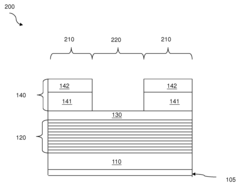
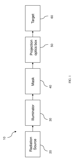
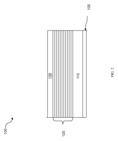
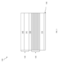
Extreme Ultraviolet (EUV) lithography systems consist of specialized components designed to work with short-wavelength light. These systems include EUV light sources, reflective optics (since EUV is absorbed by traditional lenses), specialized masks, and precise positioning stages. The integration of these components enables high-resolution semiconductor manufacturing at nanometer scales, allowing for the production of more advanced and compact integrated circuits.- EUV lithography system components and configurations: EUV lithography systems comprise specialized components designed to work with extreme ultraviolet light. These systems typically include radiation sources, illumination optics, reticle stages, projection optics, and wafer stages. The configuration of these components is critical for achieving high resolution and throughput in semiconductor manufacturing. Advanced designs incorporate vacuum environments, specialized mirrors with multilayer coatings, and precise positioning systems to handle the unique challenges of EUV wavelengths.
- EUV source technology and optimization: EUV radiation sources are critical components that generate the extreme ultraviolet light needed for lithography. These sources typically use laser-produced plasma or discharge-produced plasma technologies to create EUV radiation at 13.5nm wavelength. Innovations focus on increasing source power, stability, and conversion efficiency while reducing debris generation. Advanced cooling systems, collector optics, and plasma confinement techniques are employed to optimize source performance and extend operational lifetime.
- EUV mask technology and defect management: EUV masks (reticles) require specialized technology due to the reflective nature of EUV lithography. These masks consist of multilayer reflective coatings with absorber patterns on top. Innovations focus on defect inspection, repair techniques, and pellicle development to protect masks from contamination. Advanced pattern verification methods and compensation techniques address issues related to mask defects, pattern fidelity, and image placement accuracy to ensure high-quality pattern transfer to wafers.
- EUV resist materials and processes: Photoresist materials for EUV lithography require high sensitivity to EUV radiation while maintaining resolution, line edge roughness, and pattern collapse resistance. Chemical amplification mechanisms, metal-containing resists, and hybrid approaches are developed to address the low photon flux of EUV sources. Processing techniques include specialized development methods, post-exposure baking, and pattern transfer optimization to achieve the fine features required for advanced semiconductor nodes.
- EUV process control and computational lithography: Advanced process control techniques are essential for EUV lithography to maintain pattern fidelity and overlay accuracy. Computational lithography methods include source-mask optimization, optical proximity correction, and inverse lithography technology tailored for EUV-specific challenges. Machine learning algorithms are increasingly applied to optimize exposure parameters, predict process variations, and enhance yield. Metrology systems provide feedback for real-time process adjustments to maintain critical dimension uniformity across wafers.
02 EUV Source Technology
EUV light sources are critical components that generate the extreme ultraviolet radiation needed for lithography. These sources typically use laser-produced plasma or discharge-produced plasma technologies to create EUV radiation at 13.5nm wavelength. Innovations in this area focus on increasing source power, stability, and reliability while reducing debris generation that can contaminate optical components, thereby improving overall system throughput and performance.Expand Specific Solutions03 EUV Mask Technology
EUV masks differ significantly from traditional photomasks as they operate on reflection rather than transmission principles. These masks consist of multilayer reflective coatings with absorber patterns on top. Advancements in mask technology focus on defect inspection and repair, pattern accuracy, and reducing mask-induced imaging errors. The development of more durable and precise masks is essential for achieving the resolution and pattern fidelity required for advanced semiconductor nodes.Expand Specific Solutions04 EUV Optical Systems
Optical systems for EUV lithography employ reflective mirrors rather than refractive lenses due to the high absorption of EUV light in most materials. These systems require extremely precise multilayer-coated mirrors with near-atomic smoothness to maintain wavefront quality. Innovations focus on improving mirror reflectivity, reducing aberrations, and enhancing the numerical aperture of the optical system to achieve better resolution while maintaining adequate depth of focus for manufacturing.Expand Specific Solutions05 EUV Process Control and Integration
Process control in EUV lithography involves sophisticated methods for maintaining stability and consistency in high-volume manufacturing environments. This includes advanced metrology for alignment, focus control, and dose management. Integration challenges involve managing contamination, thermal effects, and vacuum requirements while ensuring compatibility with existing semiconductor manufacturing workflows. Solutions in this area aim to improve yield, reduce defects, and enable cost-effective implementation of EUV technology in production environments.Expand Specific Solutions
Key EUV Equipment Manufacturers and Ecosystem
EUV Lithography is currently in the growth phase of its industry lifecycle, with a rapidly expanding market projected to reach $10 billion by 2025. The technology has matured significantly, with ASML Netherlands BV establishing itself as the dominant supplier of EUV lithography systems. Key semiconductor manufacturers including Taiwan Semiconductor Manufacturing Co., Samsung Electronics, and Intel Corp. have heavily invested in EUV technology for advanced node production. Supporting ecosystem players like Carl Zeiss SMT (optical systems), Tokyo Electron (process equipment), and Lam Research (complementary tools) have developed specialized solutions to address EUV integration challenges. While the technology has achieved commercial viability for high-volume manufacturing at 7nm and below, ongoing research by companies like IBM and GlobalFoundries continues to address remaining challenges in photomask technology, resist materials, and productivity optimization.
Taiwan Semiconductor Manufacturing Co., Ltd.
Technical Solution: TSMC has been at the forefront of implementing EUV lithography in high-volume manufacturing, beginning with their 7nm+ process and expanding significantly in their 5nm and 3nm nodes. Their approach integrates EUV into a hybrid lithography strategy, using EUV for critical layers while maintaining DUV for less demanding patterns[1]. TSMC's implementation includes proprietary photoresist formulations optimized for EUV sensitivity and line edge roughness control. They've developed specialized computational models for EUV-specific effects like stochastic variations and 3D mask effects[2]. Their process integrates advanced metrology systems for defect detection and overlay control specific to EUV patterning challenges. TSMC has pioneered EUV double-patterning techniques to extend resolution beyond single-exposure limits, and implemented innovative solutions for EUV-specific challenges like pellicle integration and mask defect mitigation[3]. Their N3 (3nm) process technology utilizes over 20 EUV layers, demonstrating mastery of complex multi-patterning integration schemes.
Strengths: Industry-leading implementation of EUV in high-volume manufacturing; extensive process integration expertise; proven track record of yield management with EUV technology. Weaknesses: Heavy dependence on ASML as sole EUV equipment supplier; significant capital expenditure requirements; challenges in managing stochastic defects at advanced nodes.
Carl Zeiss SMT GmbH
Technical Solution: Zeiss SMT is the exclusive provider of optical systems for ASML's EUV lithography machines, developing the critical projection optics that enable nanometer-scale imaging. Their technology centers on all-reflective optical systems using multilayer-coated mirrors with unprecedented surface accuracy (below 100 picometers RMS)[1]. These systems incorporate up to 10 precision-engineered aspheric mirrors arranged in a complex optical train to achieve diffraction-limited performance at 13.5nm wavelength. Zeiss has pioneered advanced manufacturing techniques for ultra-precise mirror fabrication, including ion beam figuring and magnetorheological finishing that enable atomic-level surface control[2]. Their optical systems achieve Strehl ratios exceeding 0.98, approaching theoretical perfection. For next-generation high-NA EUV systems, Zeiss has developed anamorphic optical designs that provide different magnifications in x and y directions, enabling enhanced resolution while managing field size constraints[3]. Their technology includes sophisticated wavefront sensors and adaptive optics systems that maintain optical performance despite thermal and mechanical disturbances during operation.
Strengths: Unparalleled expertise in EUV optics manufacturing; proprietary metrology systems for ultra-precise surface measurement; vertical integration of critical manufacturing processes. Weaknesses: Extremely complex manufacturing processes with long lead times; limited production capacity creating potential bottlenecks; high dependence on specialized materials and coating technologies.
Critical Patents and Breakthroughs in EUV Technology
Extreme ultraviolet lithography process and mask
PatentActiveUS9448491B2
Innovation
- A mask structure incorporating a reflective multilayer with a flare-suppressing absorption stack (FSAS) and a flare-suppressing-by-phase-shifting (FSbPhS) layer, which absorbs EUV light and induces destructive interference to suppress OOB radiation, specifically DUV flare, enhancing image contrast and lithography performance.
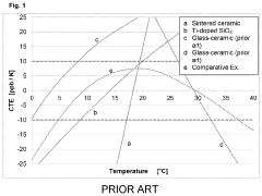
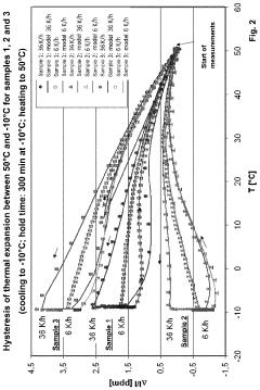
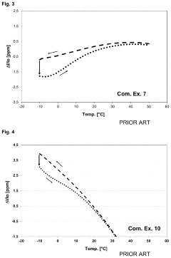
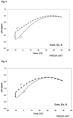
EUVL precision component with specific thermal expansion behavior
PatentPendingUS20240077798A1
Innovation
- A precision EUVL component with an average CTE of at most 0±0.1×10⁻⁶/K and thermal hysteresis of <0.1 ppm in the temperature range from 19 to 25°C, utilizing an LAS glass-ceramic composition with optimized SiO2, Li2O, and nucleating agents like TiO2, ZrO2, and WO3, which minimizes thermal hysteresis and ensures zero expansion.
Supply Chain Resilience for EUV Materials
The supply chain for Extreme Ultraviolet (EUV) lithography materials represents a critical vulnerability in the semiconductor manufacturing ecosystem. The specialized nature of EUV materials—including photoresists, pellicles, and mask blanks—creates significant challenges for maintaining consistent supply flows. Currently, these materials are produced by a limited number of suppliers globally, with heavy concentration in regions like Japan, the United States, and select European countries, creating potential bottlenecks.
Recent global disruptions, including the COVID-19 pandemic and geopolitical tensions, have exposed the fragility of the EUV materials supply chain. Semiconductor manufacturers experienced delays of up to 12-18 months for critical components, directly impacting production schedules for advanced chips utilizing EUV technology. These disruptions highlighted the need for more robust supply chain strategies specifically tailored to the unique requirements of EUV lithography.
Risk mitigation approaches being implemented across the industry include geographical diversification of suppliers, development of alternative material sources, and strategic stockpiling of critical components. Leading semiconductor manufacturers have begun establishing redundant supply networks, with some investing in vertical integration to secure access to proprietary EUV materials. ASML, the primary EUV lithography equipment manufacturer, has implemented a supplier certification program to ensure quality consistency across multiple vendors.
The development of alternative materials represents another promising avenue for enhancing supply chain resilience. Research into next-generation photoresists with reduced sensitivity to supply disruptions is advancing, with metal-oxide based formulations showing particular promise. These alternatives could potentially reduce dependence on specific rare chemicals currently essential to EUV processes.
Collaborative industry initiatives have emerged to address these challenges collectively. The Semiconductor Supply Chain Initiative (SSCI) brings together manufacturers, suppliers, and research institutions to develop standardized approaches to supply chain risk management specifically for advanced lithography materials. This includes shared early warning systems for potential disruptions and coordinated investment in alternative material development.
Looking forward, the industry is moving toward more agile and adaptive supply chain models for EUV materials. Digital twin technology is being deployed to simulate supply chain disruptions and test mitigation strategies before implementation. Additionally, blockchain-based tracking systems are being explored to enhance transparency throughout the EUV materials supply chain, enabling faster identification and resolution of potential bottlenecks.
Environmental Impact of EUV Manufacturing Processes
The manufacturing processes involved in Extreme Ultraviolet (EUV) lithography present significant environmental considerations that warrant careful examination. The production of EUV systems requires substantial energy consumption, with a single EUV lithography machine consuming approximately 1 megawatt of power during operation—roughly equivalent to the energy needs of 800 households. This intensive energy requirement contributes considerably to carbon emissions, particularly in regions where electricity generation relies heavily on fossil fuels.
Water usage represents another critical environmental concern in EUV manufacturing. The production process demands ultra-pure water in substantial quantities for cleaning silicon wafers and cooling systems. Current estimates suggest that a typical semiconductor fabrication facility utilizing EUV technology may consume between 2-4 million gallons of water daily, placing significant pressure on local water resources in manufacturing regions.
Chemical utilization in EUV processes introduces additional environmental challenges. The technology employs various hazardous substances including perfluorinated compounds (PFCs), which possess extremely high global warming potentials, and heavy metals such as tin used in plasma generation. These materials require specialized handling and disposal protocols to prevent environmental contamination.
Waste management constitutes a substantial environmental consideration for EUV manufacturing facilities. The process generates multiple waste streams including used photoresists, chemical solvents, and contaminated water that contain potentially harmful substances. Industry data indicates that a single EUV fabrication facility may produce several tons of hazardous waste monthly, necessitating sophisticated treatment systems.
Recent life cycle assessments of EUV lithography systems reveal that their environmental footprint extends beyond operational impacts. The manufacturing of precision optics, including the complex multi-layer mirrors essential to EUV technology, involves energy-intensive processes and rare earth elements with their own extraction-related environmental consequences.
The semiconductor industry has begun implementing mitigation strategies to address these environmental challenges. Leading manufacturers have established ambitious sustainability targets, including commitments to carbon neutrality, water recycling programs that achieve up to 90% water reuse rates, and chemical substitution initiatives that aim to replace the most environmentally problematic substances with greener alternatives.
Regulatory frameworks governing EUV manufacturing environmental impacts continue to evolve globally, with the European Union's Restriction of Hazardous Substances (RoHS) directive and various national semiconductor industry environmental standards establishing increasingly stringent requirements for emissions control and resource efficiency.
Unlock deeper insights with PatSnap Eureka Quick Research — get a full tech report to explore trends and direct your research. Try now!
Generate Your Research Report Instantly with AI Agent
Supercharge your innovation with PatSnap Eureka AI Agent Platform!