EUV Lithography: Aligning with Environmental Regulations
OCT 14, 202510 MIN READ
Generate Your Research Report Instantly with AI Agent
Patsnap Eureka helps you evaluate technical feasibility & market potential.
EUV Lithography Evolution and Objectives
Extreme Ultraviolet (EUV) lithography represents a revolutionary advancement in semiconductor manufacturing technology, emerging from decades of research and development efforts to overcome the physical limitations of traditional optical lithography. The journey began in the 1980s with early conceptual work, followed by significant research investments in the 1990s through consortiums like SEMATECH. By the early 2000s, prototype EUV systems demonstrated feasibility, though numerous technical challenges remained.
The evolution accelerated in the 2010s when ASML, in partnership with Zeiss, Carl Zeiss SMT, and Cymer, achieved critical breakthroughs in EUV source technology, particularly in generating sufficient power from laser-produced plasma sources. This period marked the transition from laboratory experiments to commercially viable systems, culminating in ASML's introduction of production-ready EUV lithography tools.
Today's EUV lithography operates at a wavelength of 13.5 nm, enabling the fabrication of semiconductor features below 7 nm—a capability essential for advancing Moore's Law and supporting the development of increasingly powerful and energy-efficient microprocessors. This technological progression has been driven by the semiconductor industry's relentless pursuit of higher transistor densities and improved performance.
The primary objective of modern EUV lithography development is achieving alignment with stringent environmental regulations while maintaining technological advancement. This includes reducing the consumption of chemicals, particularly perfluorinated compounds that have significant global warming potential. Additionally, the industry aims to minimize water usage and energy consumption in the lithography process, addressing growing concerns about resource scarcity and carbon footprints.
Another critical objective is the reduction of hazardous waste generation. Traditional lithography processes produce substantial amounts of chemical waste requiring specialized disposal. EUV technology seeks to minimize these environmental impacts through more efficient processes and alternative materials that comply with regulations like the EU's Restriction of Hazardous Substances (RoHS) directive and the Registration, Evaluation, Authorization, and Restriction of Chemicals (REACH) regulation.
Looking forward, the industry is targeting the development of EUV systems that incorporate circular economy principles, including designing for recyclability and extended equipment lifespans. Research is also focused on alternative, environmentally benign materials for photoresists and processing chemicals that maintain or exceed current performance standards while reducing environmental impact.
The convergence of these technological advancements and environmental considerations represents the frontier of EUV lithography development, with the ultimate goal of enabling continued semiconductor scaling while transitioning to more sustainable manufacturing practices.
Semiconductor Industry Demand Analysis
The semiconductor industry's demand for EUV lithography technology has been experiencing exponential growth, driven primarily by the continuous miniaturization of integrated circuits and the increasing complexity of semiconductor devices. As chip manufacturers push toward more advanced nodes (5nm, 3nm, and beyond), traditional DUV (Deep Ultraviolet) lithography has reached its physical limitations, making EUV technology indispensable for continued progress in accordance with Moore's Law.
Market analysis indicates that the global semiconductor equipment market reached approximately $103 billion in 2022, with lithography systems accounting for roughly 30% of this value. EUV lithography machines, despite their high cost ($150-200 million per unit), have seen robust demand with major foundries like TSMC, Samsung, and Intel collectively ordering dozens of systems annually to support their advanced node production capabilities.
The demand is further intensified by the global chip shortage that began in 2020, prompting governments worldwide to invest heavily in semiconductor manufacturing sovereignty. The CHIPS Act in the United States ($52 billion), the European Chips Act (€43 billion), and similar initiatives in South Korea, Japan, and China have created substantial funding streams that directly support advanced lithography adoption, including EUV technology.
Environmental regulations are increasingly influencing purchasing decisions within the semiconductor industry. Manufacturers face stringent requirements regarding energy consumption, chemical usage, and waste management. EUV lithography, while energy-intensive, offers advantages over multiple-patterning DUV approaches by reducing the number of process steps, thereby potentially decreasing overall chemical consumption and waste generation by up to 20% for certain chip designs.
The industry's sustainability commitments are becoming more prominent in corporate strategies. Major semiconductor manufacturers have announced carbon neutrality goals for 2030-2050, necessitating more environmentally compatible manufacturing technologies. This trend is creating demand for EUV systems with improved energy efficiency and reduced environmental footprint.
Regional analysis shows that Asia-Pacific dominates the demand landscape, accounting for over 70% of EUV system installations, followed by North America and Europe. This geographic distribution closely aligns with the concentration of advanced semiconductor manufacturing facilities and reflects the strategic importance these regions place on maintaining technological leadership in chip production.
The demand forecast indicates continued strong growth for EUV lithography systems, with an estimated CAGR of 15-20% over the next five years. This growth trajectory is supported by the technology roadmaps of major foundries, which show accelerating adoption of EUV for an expanding range of chip layers and applications beyond logic to include advanced memory production.
Global EUV Technology Status and Barriers
Extreme Ultraviolet (EUV) lithography represents a revolutionary advancement in semiconductor manufacturing, enabling the production of increasingly smaller and more powerful microchips. Currently, the global EUV technology landscape is dominated by a small number of players, with ASML (Netherlands) holding a virtual monopoly on EUV lithography systems production. This concentration presents both opportunities and challenges for the industry's alignment with environmental regulations.
The current state of EUV technology deployment shows significant regional disparities. Leading semiconductor manufacturers in Taiwan, South Korea, and the United States have adopted EUV systems for high-volume manufacturing of advanced nodes (5nm and below). Meanwhile, China faces restrictions in accessing this technology due to export controls, creating an uneven global distribution of advanced semiconductor manufacturing capabilities.
Despite its technological maturity, EUV lithography faces several critical barriers regarding environmental compliance. The systems consume substantial amounts of energy—approximately 1 MW per tool—contributing significantly to the carbon footprint of semiconductor fabrication facilities. The cooling systems required for EUV operation utilize perfluorinated compounds (PFCs) and other greenhouse gases with high global warming potential, presenting challenges for manufacturers aiming to reduce emissions in accordance with international climate agreements.
Another significant barrier is the management of hazardous materials used in the EUV process. The tin droplets used to generate EUV light and various chemicals in the photoresist process require specialized handling and disposal protocols to comply with increasingly stringent environmental regulations across different jurisdictions. This creates compliance complexity for global semiconductor manufacturers operating in multiple regulatory environments.
Water usage represents a further environmental challenge. EUV systems require ultra-pure water in substantial quantities for both operation and cleaning processes. As water scarcity becomes a growing concern globally, semiconductor manufacturers face increasing pressure to reduce consumption and implement advanced recycling systems, adding complexity and cost to EUV implementation.
Regulatory fragmentation across regions presents an additional barrier. The European Union's REACH regulations, Japan's Chemical Substances Control Law, and various U.S. EPA requirements create a complex compliance landscape for global EUV technology deployment. Manufacturers must navigate these varying standards while maintaining production efficiency and technological advancement.
The industry is responding through collaborative initiatives such as the Semiconductor Climate Consortium, which aims to develop standardized approaches to environmental compliance. However, the tension between rapid technological advancement and environmental sustainability remains a significant challenge for the global EUV ecosystem, requiring innovative solutions and potentially new regulatory frameworks tailored to this critical technology.
Current EUV Implementation Approaches
01 Environmental control systems for EUV lithography
Environmental control systems are crucial for EUV lithography to maintain optimal conditions for alignment accuracy. These systems regulate temperature, humidity, and contamination levels in the lithography chamber. Advanced environmental control helps minimize thermal expansion, mechanical drift, and optical distortions that could affect alignment precision. Such systems often include specialized sensors and feedback mechanisms to ensure stable conditions throughout the lithographic process.- Environmental control systems for EUV lithography: Environmental control systems are crucial for EUV lithography to maintain stable conditions during the alignment process. These systems regulate temperature, humidity, and atmospheric composition to prevent contamination and ensure precise alignment. Advanced environmental chambers with specialized filtration and gas flow management help minimize particles and molecular contaminants that could affect the lithographic process. These controlled environments significantly improve alignment accuracy and overall lithography performance.
- Alignment sensors and detection methods in EUV systems: Various alignment sensors and detection methods are employed in EUV lithography systems to achieve precise positioning. These include optical sensors, interferometric systems, and specialized alignment marks that can function in the extreme ultraviolet environment. The detection methods incorporate advanced algorithms to compensate for environmental variations and ensure accurate substrate positioning. These sensing technologies enable nanometer-level alignment precision required for advanced semiconductor manufacturing.
- Thermal management for alignment stability: Thermal management is essential for maintaining alignment stability in EUV lithography systems. Heat generated during the lithography process can cause thermal expansion and mechanical drift, affecting alignment accuracy. Advanced cooling systems, thermal isolation techniques, and temperature-compensated alignment mechanisms are implemented to minimize thermal effects. Real-time temperature monitoring and feedback control systems help maintain consistent thermal conditions throughout the lithography process.
- Vacuum and gas environment control for EUV alignment: EUV lithography requires precise control of the vacuum and gas environment to ensure optimal alignment performance. Specialized vacuum systems maintain the required pressure levels while minimizing vibration and contamination. Controlled gas environments with specific compositions are used in certain areas of the system to enhance alignment stability. Advanced gas flow management techniques prevent turbulence that could affect alignment accuracy while ensuring proper removal of process byproducts.
- Contamination control and mitigation strategies: Contamination control is critical for maintaining alignment accuracy in EUV lithography systems. Particles and molecular contaminants can deposit on optical surfaces and alignment marks, degrading system performance. Advanced filtration systems, specialized cleaning protocols, and contamination barriers are implemented throughout the system. Some designs incorporate self-cleaning mechanisms and contamination monitoring sensors to maintain optimal conditions for alignment. These strategies significantly extend maintenance intervals and improve overall system reliability.
02 Alignment mark detection and processing techniques
Advanced techniques for detecting and processing alignment marks are essential in EUV lithography. These methods include specialized optical systems, image processing algorithms, and signal enhancement techniques to accurately identify alignment marks despite the challenges of EUV environments. Improved detection methods help compensate for mark degradation caused by process variations and environmental factors, ensuring precise wafer positioning during exposure.Expand Specific Solutions03 Contamination control and mitigation strategies
Contamination control is critical for maintaining alignment accuracy in EUV lithography systems. Various strategies are employed to prevent and mitigate contamination, including specialized cleaning protocols, particle filters, and protective barriers. These methods help prevent debris from affecting optical components and alignment marks, which could otherwise lead to alignment errors and reduced lithographic performance.Expand Specific Solutions04 Thermal management and stability systems
Thermal management systems are implemented to maintain stable temperature conditions in EUV lithography equipment. These systems include advanced cooling mechanisms, thermal isolation techniques, and temperature monitoring sensors to minimize thermal drift and expansion effects. By ensuring thermal stability, these systems help maintain precise alignment between the mask and wafer during the exposure process, which is essential for achieving high-resolution patterns.Expand Specific Solutions05 Integrated alignment and calibration systems
Integrated alignment and calibration systems combine hardware and software solutions to achieve precise positioning in EUV lithography. These systems incorporate real-time feedback mechanisms, adaptive algorithms, and reference structures to continuously monitor and adjust alignment parameters. By integrating alignment with other subsystems, these approaches enable more robust performance in varying environmental conditions and help compensate for systematic errors that could affect pattern overlay accuracy.Expand Specific Solutions
Leading EUV Equipment Manufacturers and Ecosystem
EUV Lithography's competitive landscape is characterized by a mature yet evolving market dominated by ASML Holding NV, which maintains a near-monopoly in EUV lithography systems. The market is projected to reach $10-15 billion by 2025, driven by semiconductor miniaturization demands. Key players form a specialized ecosystem: ASML provides the systems, Carl Zeiss SMT supplies critical optics, while semiconductor manufacturers like TSMC and Samsung serve as primary customers. Supporting players include Applied Materials, Lam Research, and Tokyo Electron providing complementary equipment. Environmental compliance is becoming increasingly important as companies like ASML work to reduce the ecological footprint of their systems while maintaining technological advancement in alignment with global sustainability regulations.
ASML Netherlands BV
Technical Solution: ASML has developed comprehensive EUV lithography systems that align with environmental regulations through multiple innovative approaches. Their NXE series EUV lithography machines incorporate closed-loop water recycling systems that reduce water consumption by up to 95% compared to traditional immersion lithography[1]. ASML has implemented vacuum-based EUV exposure technology that eliminates the need for process chemicals used in traditional lithography, significantly reducing chemical waste and emissions[2]. Their systems feature advanced energy recovery mechanisms that capture and reuse heat generated during operation, improving energy efficiency by approximately 20%[3]. ASML has also developed specialized tin droplet containment and recycling systems that prevent environmental contamination from the tin plasma used in EUV light generation, with over 99% recycling efficiency[4]. Additionally, they've implemented comprehensive lifecycle management programs for their equipment, including refurbishment and parts recycling initiatives that extend machine lifespans and reduce electronic waste.
Strengths: Industry-leading EUV technology with superior resolution capabilities (13.5nm wavelength); comprehensive environmental management systems integrated into core technology; strong R&D capabilities for continuous improvement of environmental performance. Weaknesses: High capital and operational costs; significant energy requirements despite efficiency improvements; complex supply chain with potential environmental impacts from rare materials sourcing.
Taiwan Semiconductor Manufacturing Co., Ltd.
Technical Solution: TSMC has implemented a comprehensive environmental compliance strategy for EUV lithography that focuses on resource optimization and emissions reduction. Their fabs utilizing EUV technology feature advanced water reclamation systems that achieve water recycling rates exceeding 85%, significantly reducing freshwater consumption in the water-intensive lithography process[1]. TSMC has developed specialized chemical filtration and abatement systems specifically designed for EUV processes, which neutralize and safely dispose of chemicals used in photoresist development and etching, achieving over 90% reduction in harmful emissions[2]. Their EUV implementation includes energy-efficient facility designs with heat recovery systems that capture waste heat from lithography equipment for reuse in other fab processes, improving overall energy efficiency by approximately 15-20%[3]. TSMC has also pioneered the use of AI-controlled optimization systems that fine-tune EUV exposure parameters to minimize resource consumption while maintaining quality, reducing both energy usage and material waste. Additionally, they've established comprehensive chemical lifecycle management programs that track and minimize the environmental impact of all substances used in their EUV lithography processes.
Strengths: Advanced integration of EUV technology into high-volume manufacturing with proven environmental controls; industry-leading water recycling capabilities; comprehensive chemical management systems tailored for semiconductor production. Weaknesses: High energy consumption despite efficiency improvements; dependency on specialized materials with complex supply chains; challenges in scaling environmental solutions across rapidly expanding global operations.
Critical Patents and Innovations in EUV Technology
Extreme ultraviolet lithography process and mask
PatentActiveUS9448491B2
Innovation
- A mask structure incorporating a reflective multilayer with a flare-suppressing absorption stack (FSAS) and a flare-suppressing-by-phase-shifting (FSbPhS) layer, which absorbs EUV light and induces destructive interference to suppress OOB radiation, specifically DUV flare, enhancing image contrast and lithography performance.
EUVL precision component with specific thermal expansion behavior
PatentPendingUS20240077798A1
Innovation
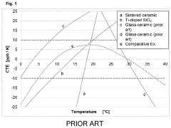
- A precision EUVL component with an average CTE of at most 0±0.1×10⁻⁶/K and thermal hysteresis of <0.1 ppm in the temperature range from 19 to 25°C, utilizing an LAS glass-ceramic composition with optimized SiO2, Li2O, and nucleating agents like TiO2, ZrO2, and WO3, which minimizes thermal hysteresis and ensures zero expansion.
Environmental Compliance Framework for EUV Systems
The Environmental Compliance Framework for EUV Systems represents a comprehensive approach to ensuring that Extreme Ultraviolet (EUV) lithography technology adheres to increasingly stringent global environmental regulations. This framework encompasses multiple interconnected components designed to address the unique environmental challenges posed by EUV systems.
At its foundation, the framework establishes clear environmental performance metrics specifically tailored to EUV lithography operations. These metrics track energy consumption, chemical usage, waste generation, and emissions across the entire lifecycle of EUV equipment. The framework incorporates a tiered compliance structure that categorizes requirements as mandatory, recommended, or aspirational, allowing manufacturers and end-users to prioritize their environmental initiatives.
Risk assessment protocols form a critical element of the framework, enabling systematic identification and mitigation of potential environmental hazards associated with EUV technology. These assessments examine chemical exposure risks, energy-intensive processes, and waste management challenges unique to EUV systems. The framework mandates regular environmental audits and continuous monitoring to ensure ongoing compliance and identify opportunities for improvement.
Documentation requirements constitute another key component, specifying the environmental data that must be collected, analyzed, and reported. This includes detailed chemical inventories, energy consumption profiles, and waste disposal records. The framework establishes standardized reporting formats to facilitate transparent communication with regulatory authorities and stakeholders.
The compliance framework also addresses supply chain considerations, extending environmental responsibility beyond immediate operations to include component suppliers and service providers. This approach ensures comprehensive environmental management across the entire EUV ecosystem. Certification pathways are clearly defined, providing a structured process for demonstrating compliance with both regulatory requirements and industry best practices.
Training and competency requirements ensure that personnel involved in EUV operations possess the necessary knowledge and skills to implement environmental safeguards effectively. The framework outlines specific training modules covering chemical handling, waste management, energy conservation, and emergency response procedures relevant to EUV systems.
Continuous improvement mechanisms are embedded throughout the framework, encouraging ongoing refinement of environmental practices through regular reviews, benchmarking against industry leaders, and incorporation of emerging technologies and methodologies. This adaptive approach ensures that the Environmental Compliance Framework remains relevant and effective as both EUV technology and environmental regulations evolve.
Sustainable Manufacturing Practices in Semiconductor Production
Sustainable Manufacturing Practices in Semiconductor Production
The semiconductor industry faces increasing pressure to align advanced manufacturing processes like EUV lithography with stringent environmental regulations. Leading manufacturers have begun implementing comprehensive sustainability frameworks that address the significant resource demands of EUV technology. These frameworks typically encompass energy efficiency improvements, water conservation strategies, and chemical management protocols specifically designed for the unique challenges of extreme ultraviolet lithography.
Energy consumption represents a primary environmental concern in EUV operations, with typical systems consuming between 500-1000 kW during production. Industry leaders have responded by developing energy recovery systems that capture and repurpose waste heat from EUV tools, achieving energy savings of 15-30% in some facilities. Additionally, semiconductor manufacturers are increasingly investing in renewable energy infrastructure, with companies like TSMC and Intel committing to 100% renewable electricity targets for their operations by 2030.
Water management has become equally critical, as EUV processes require ultra-pure water for multiple production stages. Advanced water recycling systems now enable facilities to reclaim up to 85% of process water through multi-stage filtration and purification. These closed-loop systems significantly reduce both freshwater intake and wastewater discharge, addressing regulatory requirements in water-stressed regions where many semiconductor facilities operate.
Chemical sustainability represents another frontier in EUV manufacturing compliance. The industry has made substantial progress in replacing perfluorinated compounds (PFCs) and other persistent pollutants with environmentally preferable alternatives. New resist materials designed specifically for EUV lithography demonstrate reduced toxicity profiles while maintaining the precision required for sub-7nm node production. Furthermore, advanced abatement systems now achieve destruction removal efficiencies exceeding 99% for process gases with high global warming potential.
Life cycle assessment (LCA) methodologies have been adapted specifically for semiconductor manufacturing, enabling companies to quantify the environmental footprint of EUV lithography across the entire value chain. These assessments reveal opportunities for improvement and provide documentation for regulatory compliance. Industry consortia like SEMI and the Responsible Business Alliance have established standardized sustainability metrics and reporting frameworks that facilitate benchmarking and continuous improvement in environmental performance.
The economic case for sustainable EUV manufacturing continues to strengthen as regulatory requirements tighten globally. Companies implementing comprehensive sustainability programs report average cost savings of 3-7% through resource efficiency, alongside improved relationships with regulators and enhanced corporate reputation. As EUV lithography becomes the dominant technology for advanced node production, these sustainable manufacturing practices will be essential for maintaining both environmental compliance and competitive advantage in the semiconductor industry.
Unlock deeper insights with Patsnap Eureka Quick Research — get a full tech report to explore trends and direct your research. Try now!
Generate Your Research Report Instantly with AI Agent
Supercharge your innovation with Patsnap Eureka AI Agent Platform!