

EUV Lithography: Comparative Analysis with Other Photolithography Techniques
OCT 14, 20259 MIN READ
Generate Your Research Report Instantly with AI Agent
PatSnap Eureka helps you evaluate technical feasibility & market potential.
EUV Lithography Background and Objectives
Extreme Ultraviolet (EUV) lithography represents a revolutionary advancement in semiconductor manufacturing technology, emerging as the successor to Deep Ultraviolet (DUV) lithography which had dominated the industry for decades. The development of EUV technology began in the 1990s as semiconductor manufacturers recognized the approaching physical limitations of conventional optical lithography techniques. As transistor sizes continued to shrink according to Moore's Law, the industry faced significant challenges in achieving the resolution required for sub-10nm process nodes using traditional methods.
The evolution of lithography technology has progressed through several generations, from mercury lamp-based systems operating at 436nm (g-line) and 365nm (i-line) wavelengths, to excimer laser-based DUV systems at 248nm (KrF) and 193nm (ArF). Each reduction in wavelength enabled smaller feature sizes, but by the early 2000s, it became clear that even 193nm immersion lithography with multiple patterning would eventually reach its practical limits.
EUV lithography, operating at an extremely short wavelength of 13.5nm, emerged as the most promising next-generation solution. This dramatic reduction in wavelength theoretically allows for significantly improved resolution without the complexity of multiple patterning techniques required by DUV systems at advanced nodes.
The primary objective of EUV lithography is to enable the continuation of Moore's Law by facilitating the production of increasingly smaller, more powerful, and more energy-efficient semiconductor devices. Specifically, EUV aims to achieve high-volume manufacturing of integrated circuits at the 7nm node and beyond, with a clear roadmap toward 3nm and potentially 2nm nodes.
Beyond mere miniaturization, EUV technology seeks to reduce the complexity of the lithography process by eliminating the need for multiple patterning steps required in DUV lithography at advanced nodes. This simplification promises to improve yield, reduce manufacturing costs, and accelerate time-to-market for new semiconductor products.
The development of EUV lithography has been characterized by unprecedented industry collaboration, with major semiconductor manufacturers, equipment suppliers, and research institutions working together to overcome formidable technical challenges. These include the development of reliable high-power EUV light sources, ultra-precise optics, defect-free masks, and highly sensitive photoresists.
As we analyze EUV lithography in comparison with other photolithography techniques, it is essential to understand not only its technical advantages but also the economic and strategic implications of this technology for the global semiconductor industry. EUV represents not merely an incremental improvement but a fundamental paradigm shift in semiconductor manufacturing capability, potentially reshaping competitive dynamics across the technology landscape.
Semiconductor Market Demand Analysis
The semiconductor industry has witnessed unprecedented growth in recent years, driven primarily by the increasing demand for advanced computing capabilities across various sectors. The global semiconductor market reached approximately $556 billion in 2021 and is projected to grow at a CAGR of 7.8% through 2028, highlighting the robust demand for cutting-edge semiconductor technologies.
Photolithography, particularly EUV lithography, represents a critical enabler for semiconductor manufacturing advancement. Market analysis indicates that the demand for EUV lithography systems is primarily driven by the need for smaller node sizes in logic and memory chips. The 5nm, 3nm, and upcoming 2nm process nodes require the precision that only EUV can provide, creating a substantial market pull for this technology.
Consumer electronics continue to be the largest end-user segment for advanced semiconductors, accounting for roughly 33% of the total market. The proliferation of smartphones, tablets, and other portable devices with increasingly sophisticated functionalities necessitates more powerful and energy-efficient chips that can only be manufactured using advanced lithography techniques.
The automotive sector represents the fastest-growing market segment for semiconductor demand, with a growth rate exceeding 11% annually. This surge is attributed to the increasing integration of advanced driver-assistance systems (ADAS), infotainment systems, and the transition toward electric vehicles. These applications require high-performance, reliable semiconductors that benefit from the precision manufacturing enabled by EUV lithography.
Data centers and cloud computing infrastructure constitute another significant market driver, with server chip demand growing at approximately 9% annually. The exponential increase in data processing requirements and the emergence of AI applications have intensified the need for more powerful processors with higher transistor densities, directly benefiting from EUV lithography capabilities.
Geographically, East Asia dominates semiconductor manufacturing, with Taiwan, South Korea, and Japan collectively accounting for over 60% of global production capacity. However, recent geopolitical tensions and supply chain vulnerabilities have accelerated initiatives in the US and Europe to establish domestic semiconductor manufacturing capabilities, creating new market opportunities for EUV lithography equipment suppliers.
The transition from traditional DUV to EUV lithography represents a significant market inflection point. While the initial capital investment for EUV equipment is substantially higher (approximately $120-150 million per tool versus $40-60 million for advanced DUV tools), the long-term economic benefits in terms of yield, performance, and power efficiency create compelling market incentives for adoption at advanced nodes.
EUV Technology Status and Challenges
Extreme Ultraviolet (EUV) lithography represents the cutting edge of semiconductor manufacturing technology, operating at a wavelength of 13.5nm. Currently, ASML holds a virtual monopoly in the EUV equipment market, with their systems deployed in leading semiconductor fabrication facilities worldwide. The technology has successfully entered mass production phase since 2019, with companies like TSMC, Samsung, and Intel incorporating EUV processes in their advanced node manufacturing.
Despite its commercial deployment, EUV technology faces significant technical challenges. The generation of sufficient EUV light remains problematic, with current power sources achieving only 250-300W compared to the ideal 500W required for optimal throughput. This power limitation directly impacts production efficiency and economic viability. Additionally, the creation of defect-free photomasks presents a substantial hurdle, as even nanoscale imperfections can cause critical pattern failures.
EUV systems also struggle with photoresist performance issues. Current photoresists face a fundamental trade-off between sensitivity, resolution, and line edge roughness—the so-called "triangle of death" in lithography. Researchers continue to develop new photoresist chemistries to overcome these limitations, but progress has been incremental rather than revolutionary.
From a geographical perspective, EUV technology development is concentrated in specific regions. The Netherlands houses ASML's manufacturing capabilities, while Japan leads in supporting components such as mirrors and masks. The United States contributes significantly to light source technology, and South Korea and Taiwan serve as primary implementation sites due to their semiconductor manufacturing prowess.
Infrastructure requirements present another major challenge. EUV systems demand extraordinary precision in environmental control, requiring specialized facilities with exceptional vibration isolation, temperature stability, and vacuum systems. The complexity of these requirements has limited adoption to only the most advanced semiconductor manufacturers.
Economic barriers further constrain EUV implementation. With each lithography system costing approximately $150-200 million, plus substantial operational expenses, only high-volume manufacturers can justify the investment. This has created a technological divide in the semiconductor industry, with only a handful of companies capable of deploying EUV technology at scale.
Looking forward, stochastic effects at sub-7nm nodes present perhaps the most fundamental challenge. As feature sizes approach atomic scales, random variations in photon absorption and chemical reactions introduce unpredictable defects, potentially limiting the ultimate resolution achievable with EUV technology.
Current EUV Implementation Solutions
01 EUV Lithography System Design and Components
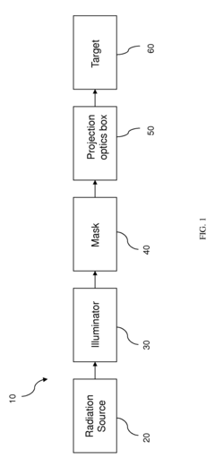
EUV lithography systems incorporate specialized components designed to work with extreme ultraviolet light. These systems include illumination optics, projection optics, and reflective masks that operate in vacuum environments. The design focuses on achieving high resolution patterning while managing the challenges of working with short wavelength EUV radiation. Advanced optical elements and precise positioning mechanisms are essential for maintaining imaging accuracy at nanometer scales.- EUV Lithography System Components: Extreme Ultraviolet (EUV) lithography systems consist of specialized components designed to work with short-wavelength light. These systems include EUV light sources, reflective optics (since EUV light is absorbed by traditional lenses), specialized masks, and precision positioning stages. The integration of these components enables high-resolution semiconductor manufacturing at nanometer scales, allowing for the production of more advanced and compact integrated circuits.
- EUV Source Technology: EUV light sources are critical components that generate the extreme ultraviolet radiation needed for lithography. These sources typically use laser-produced plasma or discharge-produced plasma technologies to create EUV radiation at a wavelength of 13.5nm. The development of high-power, stable EUV sources has been essential for making EUV lithography commercially viable, as they must provide sufficient power while maintaining stability for precise pattern transfer.
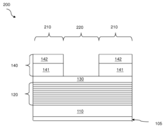
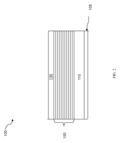
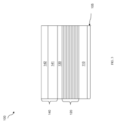
- EUV Mask Technology: EUV masks differ significantly from traditional photomasks as they operate on reflection rather than transmission principles. These masks consist of multilayer reflective coatings with absorber patterns that define the circuit features. The development of defect-free masks with precise patterns is crucial for accurate pattern transfer. Advanced inspection and repair technologies are employed to ensure mask quality, which directly impacts the final semiconductor device performance.
- EUV Process Control and Optimization: Controlling and optimizing the EUV lithography process involves sophisticated metrology, alignment systems, and computational techniques. Process control systems monitor and adjust various parameters to maintain consistency and accuracy in pattern transfer. Optimization techniques include optical proximity correction, source mask optimization, and various computational lithography approaches that enhance resolution and pattern fidelity while compensating for process variations.
- EUV Integration and Manufacturing Solutions: The integration of EUV lithography into semiconductor manufacturing requires specialized solutions for contamination control, vacuum systems, and thermal management. Manufacturing solutions include cluster tools that integrate multiple process steps, automated material handling systems, and comprehensive factory control software. These integrated approaches help manage the complexity of EUV lithography while maximizing throughput and yield in high-volume manufacturing environments.
02 Contamination Control and Protection Methods
Contamination control is critical in EUV lithography due to the sensitivity of optical components to particles and molecular contaminants. Various protection methods are employed including specialized cleaning techniques, contamination barriers, and environmental control systems. These methods help prevent degradation of reflective surfaces and maintain consistent performance of the lithography system over time, ensuring reliable pattern transfer at extreme resolutions.Expand Specific Solutions03 EUV Source Technology and Optimization
EUV source technology focuses on generating sufficient power at the 13.5nm wavelength required for lithography. This includes plasma-based sources using tin or other materials that emit EUV radiation when excited. Source optimization involves improving conversion efficiency, stability, and reducing debris generation. Advanced collector designs and plasma confinement techniques help maximize the useful EUV output while maintaining operational reliability for high-volume manufacturing environments.Expand Specific Solutions04 Resist Materials and Process Chemistry
Specialized resist materials are developed for EUV lithography to achieve high sensitivity, resolution, and pattern fidelity. These materials must respond efficiently to EUV photons while maintaining low line edge roughness and high etch resistance. Process chemistry innovations include novel development techniques, underlayers, and topcoat materials that enhance performance. Optimization of resist formulations addresses the unique challenges of EUV exposure including stochastic effects and secondary electron generation.Expand Specific Solutions05 Computational Lithography and Pattern Optimization
Computational methods play a crucial role in EUV lithography to enhance imaging performance. These include optical proximity correction, source mask optimization, and inverse lithography techniques adapted for EUV-specific challenges. Advanced modeling accounts for EUV-specific phenomena such as shadowing effects, flare, and non-telecentricity. Machine learning approaches are increasingly applied to optimize patterns and process windows, improving yield and enabling more complex semiconductor device structures at smaller nodes.Expand Specific Solutions
Key Industry Players in EUV Ecosystem
EUV Lithography is currently in the growth phase of its industry lifecycle, with a rapidly expanding market projected to reach $10-15 billion by 2025. The technology has matured significantly but remains at the cutting edge of semiconductor manufacturing. ASML Netherlands BV dominates the EUV equipment market as the sole supplier of production-ready EUV lithography systems, while Taiwan Semiconductor Manufacturing Co. (TSMC) and Samsung Electronics lead in implementation. Intel and GlobalFoundries are investing heavily to catch up. Supporting ecosystem players include Applied Materials, Lam Research, and Tokyo Electron providing complementary tools, while materials suppliers like AGC and Shin-Etsu Chemical develop specialized photoresists and optical components. The technology represents a critical enabler for advanced semiconductor nodes below 7nm.
Taiwan Semiconductor Manufacturing Co., Ltd.
Technical Solution: TSMC has pioneered the implementation of EUV lithography in high-volume manufacturing, beginning with their 7nm+ process and expanding to 5nm and 3nm nodes. Their approach integrates EUV with multi-patterning techniques to optimize cost and performance. TSMC's EUV implementation includes custom-designed computational lithography solutions that compensate for mask 3D effects and stochastic variations inherent to EUV. They've developed specialized resist materials with their chemical suppliers that balance sensitivity, resolution, and line edge roughness. TSMC has created a comprehensive defect detection and control system specifically for EUV layers, using advanced inspection tools and machine learning algorithms to identify and classify defects. Their fab design incorporates specialized clean room environments with enhanced vibration control and temperature stability to maximize EUV tool performance and uptime. TSMC has reported achieving over 90% availability for their EUV systems, significantly higher than early industry implementations[3][4].
Strengths: Industry-leading implementation expertise; optimized integration with existing processes; demonstrated high-volume manufacturing capability; superior defect control systems. Weaknesses: Extremely high capital expenditure requirements; complex process integration challenges; dependency on limited EUV equipment suppliers; ongoing challenges with EUV mask infrastructure.
ASML Netherlands BV
Technical Solution: ASML is the dominant supplier of EUV lithography equipment, holding over 90% market share in advanced lithography tools. Their NXE series EUV systems operate at 13.5nm wavelength using a laser-produced plasma source that generates EUV light when high-power CO2 lasers hit tin droplets. The latest NXE:3600D system achieves resolution below 13nm with 170 wafers per hour throughput and overlay accuracy of 1.1nm. ASML's EUV technology incorporates sophisticated computational lithography, including optical proximity correction and source mask optimization to enhance pattern fidelity. Their systems use reflective optics with multilayer mirrors rather than traditional refractive optics due to EUV's strong absorption by most materials. ASML has developed specialized vacuum systems, contamination control, and pellicle technology to protect masks from particles[1][2].
Strengths: Unmatched resolution capability enabling sub-7nm node manufacturing; significantly reduced multi-patterning requirements compared to DUV; higher pattern fidelity for complex designs. Weaknesses: Extremely high tool costs ($150-200M per tool); lower throughput compared to mature DUV systems; higher energy consumption; complex infrastructure requirements including vacuum systems.
Critical EUV Patents and Technical Innovations
Extreme ultraviolet lithography process and mask
PatentActiveUS9448491B2
Innovation
- A mask structure incorporating a reflective multilayer with a flare-suppressing absorption stack (FSAS) and a flare-suppressing-by-phase-shifting (FSbPhS) layer, which absorbs EUV light and induces destructive interference to suppress OOB radiation, specifically DUV flare, enhancing image contrast and lithography performance.
EUVL precision component with specific thermal expansion behavior
PatentPendingUS20240077798A1
Innovation
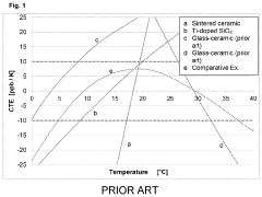
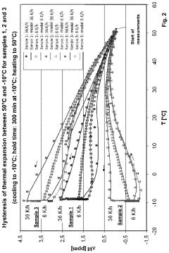
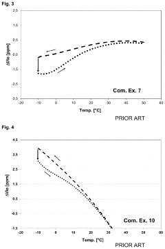
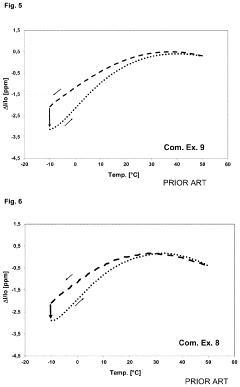
- A precision EUVL component with an average CTE of at most 0±0.1×10⁻⁶/K and thermal hysteresis of <0.1 ppm in the temperature range from 19 to 25°C, utilizing an LAS glass-ceramic composition with optimized SiO2, Li2O, and nucleating agents like TiO2, ZrO2, and WO3, which minimizes thermal hysteresis and ensures zero expansion.
Supply Chain Dependencies and Risks
The EUV lithography supply chain represents one of the most complex and vulnerable technological ecosystems in the semiconductor industry. Unlike conventional photolithography techniques, EUV relies on a highly specialized and concentrated supplier network, creating significant dependencies and risks. The Netherlands-based ASML maintains a virtual monopoly on EUV lithography systems, making the entire global semiconductor industry dependent on a single source for this critical technology.
Raw material constraints present another major vulnerability. EUV systems require specialized materials including high-purity germanium for optics and specific noble gases for laser operation. These materials often originate from geopolitically sensitive regions, creating potential bottlenecks during international tensions or trade disputes. The COVID-19 pandemic demonstrated how quickly these supply chains can be disrupted, with lead times for EUV systems extending from months to years.
Geopolitical factors significantly impact the EUV supply chain. Export controls and technology restrictions between major economies have created artificial barriers in what should be a global technology ecosystem. The United States, Japan, and the Netherlands have implemented coordinated export controls on advanced lithography equipment to certain markets, fragmenting the global semiconductor manufacturing landscape and potentially accelerating technological divergence.
Technical knowledge transfer represents another critical dependency. The expertise required for EUV implementation is concentrated among a small group of engineers and scientists globally. This human capital bottleneck creates significant risks as the industry attempts to scale EUV adoption. Unlike DUV (Deep Ultraviolet) lithography, where knowledge has diffused globally over decades, EUV expertise remains concentrated in a few geographic clusters.
Financial risks also characterize the EUV supply chain. The extreme cost of EUV systems (exceeding $150 million per unit) creates significant capital expenditure requirements that only the largest semiconductor manufacturers can sustain. This financial barrier reinforces industry consolidation and potentially limits innovation from smaller players who cannot access the technology.
When compared to other lithography techniques, EUV's supply chain is significantly more vulnerable. DUV lithography benefits from multiple equipment suppliers (including Nikon and Canon alongside ASML) and more mature, diversified supply chains. Similarly, older i-line and g-line technologies feature commoditized equipment with minimal supply risks. This contrast highlights how advancing to more sophisticated lithography techniques inherently increases supply chain vulnerability.
Environmental Impact and Sustainability Considerations
The environmental footprint of semiconductor manufacturing processes has become increasingly significant as the industry advances. EUV lithography, while representing a technological breakthrough, presents distinct environmental challenges compared to previous photolithography techniques. The energy consumption of EUV systems is substantially higher than that of traditional DUV (Deep Ultraviolet) systems, with a single EUV tool consuming up to 1 MW of power during operation—approximately 2-3 times more than immersion lithography tools.
Water usage represents another critical environmental concern. EUV systems require ultra-pure water for cooling and cleaning processes, with consumption rates estimated at 5,000-7,000 liters per hour during peak operation. This exceeds the requirements of previous generation tools by approximately 40%, placing additional strain on local water resources in semiconductor manufacturing regions.
Chemical waste management differs significantly between lithography technologies. While EUV reduces the need for certain process chemicals used in multiple patterning approaches, it introduces new challenges related to tin debris management from the plasma source and specialized cleaning agents for EUV-specific components. The environmental persistence and toxicity profiles of these materials require careful consideration in waste management protocols.
Greenhouse gas emissions associated with EUV manufacturing and operation present a complex sustainability challenge. The production of specialized components, particularly the highly precise mirrors requiring dozens of alternating molybdenum and silicon layers, involves energy-intensive processes with substantial carbon footprints. Additionally, the gases used in EUV chambers, while smaller in volume than those in traditional systems, often have higher global warming potentials.
From a lifecycle perspective, EUV tools demonstrate interesting sustainability trade-offs. Their extended operational lifespan potentially reduces manufacturing waste associated with frequent equipment replacement. However, the complexity of EUV systems complicates end-of-life recycling and material recovery efforts compared to simpler lithography technologies.
Leading semiconductor manufacturers have implemented various sustainability initiatives specifically addressing EUV environmental impacts. These include energy recovery systems that capture waste heat from EUV tools, closed-loop water recycling technologies that reduce freshwater consumption by up to 60%, and advanced abatement systems for process emissions. Industry consortia have also established specialized recycling programs for critical EUV components, particularly the high-value optics containing rare materials.
Regulatory frameworks governing semiconductor manufacturing environmental impacts continue to evolve, with particular attention to the unique challenges posed by advanced lithography. Compliance requirements vary significantly by region, creating complex operational considerations for global semiconductor manufacturers deploying EUV technology across multiple facilities.
Unlock deeper insights with PatSnap Eureka Quick Research — get a full tech report to explore trends and direct your research. Try now!
Generate Your Research Report Instantly with AI Agent
Supercharge your innovation with PatSnap Eureka AI Agent Platform!