EUV Lithography: Technical Insights into Reflective Optics
OCT 14, 20259 MIN READ
Generate Your Research Report Instantly with AI Agent
Patsnap Eureka helps you evaluate technical feasibility & market potential.
EUV Lithography Evolution and Objectives
Extreme Ultraviolet (EUV) lithography represents a revolutionary advancement in semiconductor manufacturing technology, marking a significant departure from traditional optical lithography methods. The evolution of EUV technology spans several decades, beginning in the 1980s with initial research into short-wavelength lithography techniques. By utilizing 13.5nm wavelength light, EUV lithography enables the production of semiconductor devices with feature sizes below 7nm, addressing the limitations of previous deep ultraviolet (DUV) lithography systems.
The development trajectory of EUV lithography has been characterized by persistent technical challenges and breakthrough innovations. Early research focused primarily on light source development, with significant milestones achieved in the late 1990s through the creation of laser-produced plasma (LPP) and discharge-produced plasma (DPP) sources. The 2000s witnessed critical advancements in reflective optics technology, as traditional refractive optics proved ineffective at EUV wavelengths due to extreme absorption issues.
By 2010, major semiconductor equipment manufacturers had demonstrated prototype EUV systems, though productivity and reliability remained significant hurdles. The period between 2010 and 2018 saw intensive engineering efforts to overcome these challenges, culminating in the first commercial deployment of EUV lithography systems in high-volume manufacturing environments. This transition represented the realization of decades of research and development investment.
The technical objectives of EUV lithography center on enabling continued semiconductor scaling according to Moore's Law while overcoming the physical limitations of traditional optical lithography. Specific goals include achieving resolution capabilities below 10nm, maintaining acceptable throughput rates of at least 100-125 wafers per hour, and ensuring sufficient overlay accuracy to support multi-patterning techniques. Additionally, EUV systems aim to reduce the complexity of multiple patterning processes required by previous technologies.
Current research focuses on extending EUV capabilities through high numerical aperture (High-NA) systems, which promise to enable feature sizes down to 3nm and beyond. These next-generation systems target increased resolution through larger optical elements and more sophisticated reflective designs. Concurrent development efforts address power scaling challenges to improve throughput rates, as well as resist chemistry optimization to enhance pattern fidelity and reduce defectivity.
The evolution of EUV lithography exemplifies the semiconductor industry's commitment to overcoming seemingly insurmountable technical barriers through sustained research investment and cross-disciplinary collaboration. As the technology continues to mature, its objectives expand beyond mere resolution enhancement to encompass cost-effectiveness, reliability, and integration with complementary technologies in the semiconductor manufacturing ecosystem.
Semiconductor Industry Demand for EUV Technology
The semiconductor industry's demand for Extreme Ultraviolet (EUV) lithography technology has been driven by the relentless pursuit of Moore's Law, which predicts the doubling of transistor density approximately every two years. As conventional deep ultraviolet (DUV) lithography approaches its physical limits around the 7nm node, EUV has emerged as the critical enabler for continued miniaturization in advanced semiconductor manufacturing.
Market analysis reveals that the global semiconductor industry, valued at over $550 billion, is increasingly dependent on EUV technology to maintain competitive advantages in high-performance computing, mobile devices, and emerging applications like artificial intelligence and autonomous vehicles. Leading foundries and integrated device manufacturers have committed substantial investments to EUV implementation, with TSMC, Samsung, and Intel collectively allocating tens of billions of dollars toward EUV-capable fabrication facilities.
The demand for EUV lithography systems is particularly acute in the manufacturing of logic chips at 7nm nodes and below, where multi-patterning techniques using DUV become economically prohibitive due to increased process steps and yield challenges. Industry reports indicate that EUV adoption reduces mask complexity by 25-40% compared to multi-patterning approaches, translating to significant cost savings despite the high initial investment in EUV equipment.
Memory manufacturers have also begun integrating EUV technology into their production lines, particularly for DRAM devices requiring increasingly precise pattern definition. This expansion beyond logic chips represents a substantial growth vector for EUV technology adoption, with memory manufacturers expected to account for approximately 30% of EUV system installations by 2025.
The geographical distribution of EUV demand follows the concentration of advanced semiconductor manufacturing, with East Asia (particularly Taiwan, South Korea, and increasingly China) representing the largest market, followed by the United States and Europe. Recent geopolitical tensions and supply chain concerns have accelerated initiatives in the US and Europe to establish domestic advanced semiconductor manufacturing capabilities, further stimulating regional demand for EUV systems.
Industry forecasts project the EUV lithography equipment market to grow at a compound annual growth rate exceeding 20% through 2026, reflecting both the expansion of existing EUV-capable fabs and the construction of new facilities. This growth trajectory is supported by the technology roadmaps of major semiconductor manufacturers, which increasingly position EUV as essential for nodes at 5nm and below, where the economic and technical advantages over alternative lithography approaches become decisive.
Reflective Optics Challenges in EUV Implementation
The implementation of Extreme Ultraviolet (EUV) lithography represents a significant technological leap in semiconductor manufacturing, enabling the production of increasingly smaller transistors. However, the reflective optics system at the heart of EUV technology presents several formidable challenges that continue to impact its widespread adoption and performance optimization.
One of the primary challenges lies in the fundamental physics of EUV light interaction with materials. At the 13.5nm wavelength used in EUV lithography, virtually all materials are highly absorptive, necessitating the use of reflective optics rather than traditional transmissive lenses. These reflective systems require multilayer mirrors composed of alternating layers of molybdenum and silicon, each only a few nanometers thick, to achieve maximum reflectivity of approximately 70% per mirror.
The manufacturing precision required for these mirrors presents extraordinary difficulties. Surface roughness must be controlled to less than 0.1nm RMS (root mean square), which is approximately the size of a single atom. Any deviation beyond this tolerance significantly reduces reflectivity and introduces wavefront errors that degrade image quality. The fabrication process involves advanced polishing techniques, ion beam figuring, and metrology systems operating at unprecedented precision levels.
Thermal management constitutes another critical challenge in EUV reflective optics. The intense energy of EUV radiation causes heating in the mirror substrates, leading to thermal expansion and distortion of the optical surfaces. Even nanometer-scale distortions can significantly impact imaging performance. Sophisticated cooling systems and thermally stable materials like ultra-low expansion glass are essential, yet thermal gradients remain difficult to eliminate entirely.
Contamination control represents a persistent obstacle in maintaining reflective optics performance. Carbon contamination from residual hydrocarbons in the vacuum environment can accumulate on mirror surfaces, reducing reflectivity over time. Similarly, tin debris from the plasma source can deposit on the collector mirror. These contamination issues necessitate complex in-situ cleaning technologies and protective measures that add to system complexity.
The optical design itself faces inherent limitations due to the limited number of mirrors that can be used. Each mirror in the optical path reduces overall system transmission by approximately 30%, creating a trade-off between optical performance and throughput. Most EUV systems employ between 8-11 mirrors, resulting in significant light loss through the optical train and constraining the numerical aperture achievable in production systems.
Long-term stability of reflective coatings presents ongoing reliability concerns. The intense radiation environment, thermal cycling, and potential chemical interactions can degrade mirror performance over time. Developing coatings that maintain consistent reflectivity throughout the operational lifetime of EUV systems remains an active area of research and development.
Current Reflective Optics Solutions for EUV
01 Multilayer reflective coatings for EUV lithography
Multilayer reflective coatings are essential components in EUV lithography systems, typically consisting of alternating layers of materials with high and low refractive indices. These coatings are designed to maximize reflectivity at EUV wavelengths (around 13.5 nm). Common material combinations include molybdenum/silicon (Mo/Si) layers, which can achieve reflectivity values of over 65%. The precise thickness control and interface engineering of these multilayers are critical for maintaining high reflectivity performance in EUV optical systems.- Multilayer reflective coatings for EUV optics: Multilayer reflective coatings are essential components in EUV lithography systems, typically consisting of alternating layers of high and low refractive index materials. These coatings are designed to maximize reflectivity at EUV wavelengths (around 13.5nm). The multilayer structure often includes materials like molybdenum and silicon, with precise thickness control to achieve constructive interference. Advanced coating techniques help minimize defects and ensure uniform reflectivity across the optical surface, which is critical for maintaining image quality in EUV lithography systems.
- Optical system design for EUV lithography: EUV lithography systems employ specialized optical designs to manage the unique challenges of extreme ultraviolet light. These systems typically use all-reflective optics arranged in specific configurations to minimize aberrations and maximize throughput. The optical path often includes multiple mirrors with aspheric surfaces to correct for distortions. Design considerations include minimizing the number of reflections (as each reflection reduces intensity), managing thermal effects, and maintaining precise alignment between optical elements to achieve the nanometer-scale resolution required for advanced semiconductor manufacturing.
- Contamination control and protection systems: Contamination control is critical in EUV lithography systems as even nanometer-scale particles can cause defects in the printed patterns. Protection systems include specialized environmental controls, gas purging mechanisms, and barrier layers to prevent carbon contamination and oxidation of reflective surfaces. Some systems incorporate hydrogen or other cleaning gases to remove carbon deposits that form during operation. Advanced monitoring systems detect contamination in real-time, allowing for maintenance before performance degradation occurs. These protection measures are essential for maintaining the reflectivity of optical components and extending their operational lifetime.
- Thermal management and stability control: EUV lithography systems require sophisticated thermal management to maintain optical performance, as even nanometer-scale thermal expansions can affect imaging quality. Cooling systems are integrated with reflective optics to dissipate heat generated by EUV radiation absorption. Active temperature control systems maintain optical elements at precise operating temperatures. Some designs incorporate low thermal expansion materials or compensation mechanisms to minimize distortion. Vibration isolation systems are also employed to prevent mechanical disturbances from affecting the optical path, ensuring stable imaging performance during operation.
- Manufacturing and metrology of EUV reflective optics: Manufacturing EUV reflective optics requires ultra-precision fabrication techniques to achieve the necessary surface quality. Advanced polishing methods produce mirror substrates with surface roughness below 0.1nm RMS. Metrology systems, including interferometry and atomic force microscopy, verify surface specifications at atomic scales. Coating processes must ensure uniform layer thickness across the entire optical surface. Post-manufacturing characterization includes reflectivity measurements, wavefront error analysis, and accelerated lifetime testing. These manufacturing challenges are addressed through specialized equipment and processes developed specifically for EUV optical components.
02 Contamination control and protection systems
EUV lithography systems require sophisticated contamination control mechanisms to maintain the performance of reflective optics. These include protective capping layers, gas curtains, and plasma cleaning techniques to prevent carbon contamination and oxidation of mirror surfaces. Hydrogen or other cleaning gases are often used to remove carbon deposits, while specialized barrier layers protect the multilayer structures from environmental degradation. These protection systems are crucial for extending the lifetime of EUV optical components in high-volume manufacturing environments.Expand Specific Solutions03 Thermal management for EUV reflective optics
Thermal management is critical in EUV lithography systems as the intense radiation can cause heating and subsequent distortion of reflective optics. Advanced cooling systems, including liquid cooling channels and thermally conductive substrates, are employed to maintain dimensional stability. Additionally, materials with matched thermal expansion coefficients are selected to minimize stress and deformation under thermal load. Active thermal control systems continuously monitor and adjust temperature distributions to maintain nanometer-level precision during operation.Expand Specific Solutions04 Substrate materials and fabrication for EUV mirrors
Specialized substrate materials with exceptional surface finish and stability are required for EUV reflective optics. Ultra-low expansion glass, silicon carbide, and zerodur are commonly used materials that provide the necessary dimensional stability. Advanced polishing techniques achieve surface roughness below 0.2 nm RMS, while ion beam figuring allows for atomic-level corrections to the mirror surface profile. The substrate fabrication process must maintain figure accuracy within nanometer tolerances while supporting the multilayer coating structure.Expand Specific Solutions05 Optical design and aberration correction
EUV lithography systems employ complex optical designs with multiple reflective elements to minimize aberrations while maintaining high numerical aperture. Aspheric mirror surfaces, often with freeform geometries, are used to correct for optical aberrations inherent in reflective systems. Wavefront sensing and adaptive optics technologies enable real-time correction of dynamic aberrations during operation. The optical design must balance competing requirements of field size, resolution, and light throughput while accommodating the limited reflectivity of each surface in the optical path.Expand Specific Solutions
Leading Companies in EUV Lithography Ecosystem
EUV Lithography's competitive landscape is characterized by a mature yet evolving market dominated by key players in different segments of the value chain. ASML Netherlands BV holds a near-monopoly in EUV lithography systems manufacturing, while Carl Zeiss SMT GmbH leads in reflective optics development. The market is supported by specialized materials suppliers like Shin-Etsu Chemical and AGC, with semiconductor giants including TSMC, Samsung, and Intel driving demand as primary end-users. The technology has reached commercial maturity but continues to evolve, with market size estimated at $5-7 billion annually and growing. Competition focuses on improving resolution capabilities, reducing defects, and enhancing throughput to meet the semiconductor industry's demands for increasingly smaller nodes.
Carl Zeiss SMT GmbH
Technical Solution: Carl Zeiss SMT has developed the most advanced reflective optical systems for EUV lithography, focusing on precision-engineered multi-layer mirrors that form the core of the projection optics box (POB). Their mirrors utilize alternating layers of molybdenum and silicon deposited with atomic precision, achieving reflectivity rates of approximately 70% at the 13.5nm wavelength. Each mirror substrate is manufactured from ultra-low expansion glass, polished to a surface roughness of less than 0.1nm RMS, and shaped with aspheric precision to control wavefront errors within picometer tolerances. Zeiss's proprietary ion beam figuring technology enables surface corrections at the atomic level, while their integrated metrology systems provide real-time feedback during manufacturing. The company has pioneered computational optics techniques that predict and compensate for thermal and mechanical distortions during operation. Their latest innovation includes the development of High-NA (0.55) optical systems that will enable feature sizes below 8nm, requiring even more complex mirror geometries with steeper angles and tighter tolerances.
Strengths: Unmatched expertise in precision optics manufacturing; proprietary polishing and metrology technologies; exclusive partnership with ASML for EUV systems. Weaknesses: Extremely capital-intensive production process; limited production capacity creating potential bottlenecks; complete dependency on ASML as the primary customer.
Nikon Corp.
Technical Solution: Nikon has developed its own approach to EUV lithography reflective optics, though not yet commercialized at the same scale as ASML. Their system architecture employs a multi-mirror optical train with proprietary coating technology optimized for the 13.5nm wavelength. Nikon's reflective optics design incorporates between 6-8 precision-engineered aspheric mirrors arranged in a specific sequence to minimize aberrations while maintaining high numerical aperture. Their mirrors utilize molybdenum-silicon multilayer coatings with precisely controlled thickness variations across the mirror surface to compensate for angle-dependent reflectivity effects. Nikon has invested significantly in computational optics to simulate and optimize the entire optical path, accounting for thermal effects and mechanical stresses during operation. Their approach includes innovative mirror mounting systems that isolate the optics from vibration while allowing for thermal expansion. Nikon has also developed specialized metrology tools capable of measuring surface accuracy to the picometer level, essential for manufacturing and qualifying EUV optical components. While not currently offering commercial EUV systems, Nikon maintains active research programs in this field.
Strengths: Extensive experience in lithography systems; strong optical design capabilities; established relationships with semiconductor manufacturers. Weaknesses: Significantly behind ASML in commercialization; lacks the complete ecosystem integration; limited market acceptance of their EUV approach.
Critical Patents in EUV Reflective Optics
Extreme ultraviolet mask with backside coating
PatentWO2020086932A1
Innovation
- A backside coating layer comprising an alloy of tantalum and nickel is applied to the EUV mask blank, providing improved hardness, durability, and reduced thickness, along with suitable coefficient of friction and optical density, which reduces defect rates and enhances the EUV mask blank's performance.


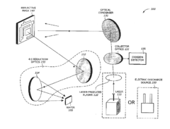
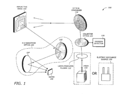
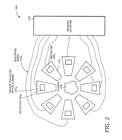
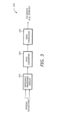
Detecting erosion in collector optics with plasma sources in extreme ultraviolet (EUV) lithography systems
PatentInactiveUS6841322B1
Innovation
- A system that detects erosion in the ML coating of EUVL stepper and optical systems by measuring initial and coating impedances over time, determining the erosion rate, and monitoring it in-situ to timely replace eroded collectors, using a combination of impedance measuring circuits, data converters, and data processors to initiate warnings and replacements.
Materials Science Advancements for EUV Mirrors
The advancement of materials science has been pivotal in overcoming the significant challenges associated with EUV mirror development. Traditional optical materials used in conventional lithography systems are inadequate for EUV wavelengths (13.5 nm), necessitating the development of specialized multilayer reflective coatings. Molybdenum-silicon (Mo/Si) multilayer structures have emerged as the industry standard, achieving reflectivity rates of approximately 70% at the target wavelength.
Recent breakthroughs in material composition have focused on interface engineering between the Mo and Si layers. Researchers have successfully implemented diffusion barrier layers of only a few atoms thick, typically composed of boron carbide (B4C) or ruthenium (Ru), which significantly reduce interdiffusion effects and enhance reflectivity by up to 3-4% compared to earlier generations.
Surface roughness control has seen remarkable progress, with current state-of-the-art mirrors achieving atomic-level smoothness with root mean square (RMS) roughness values below 0.15 nm. This advancement has been made possible through novel polishing techniques including ion beam figuring and chemical mechanical polishing (CMP) specifically optimized for EUV mirror substrates.
Thermal stability remains a critical challenge as EUV mirrors must maintain nanometer-level precision under intense radiation exposure. Innovative cooling systems incorporating microchannels etched directly into mirror substrates have demonstrated superior heat dissipation capabilities. Additionally, the incorporation of thermally stable capping layers, particularly ruthenium-based compounds, has improved resistance to oxidation and carbon contamination during operation.
Material scientists have also addressed the issue of radiation damage through the development of self-healing coating architectures. These advanced structures incorporate trace amounts of mobile atoms that can migrate to radiation-induced defect sites, effectively restoring the multilayer structure during operation and extending mirror lifetime by up to 40% in laboratory conditions.
Looking forward, promising research directions include the exploration of alternative material pairs beyond Mo/Si, such as ruthenium/silicon (Ru/Si) and lanthanum/boron (La/B) multilayers, which theoretically offer higher theoretical reflectivity at specific EUV wavelengths. Additionally, atomic layer deposition (ALD) techniques are being refined to enable precise control over layer thickness with sub-angstrom accuracy, potentially enabling the next generation of higher-performance EUV mirrors with reflectivity approaching 75%.
Economic Impact of EUV Technology Adoption
The adoption of Extreme Ultraviolet (EUV) lithography represents a watershed moment in semiconductor manufacturing, with profound economic implications across the global technology ecosystem. Initial investments in EUV technology have been substantial, with leading semiconductor manufacturers allocating billions of dollars to integrate these advanced systems into their production lines. ASML, the sole supplier of EUV lithography machines, prices each system at approximately $150-200 million, creating a significant capital expenditure barrier for market entry.
Despite these high initial costs, economic analyses indicate compelling long-term returns on investment. Companies implementing EUV lithography have reported 20-30% reductions in overall chip production costs at advanced nodes (7nm and below) when factoring in the elimination of multiple patterning steps required by previous DUV (Deep Ultraviolet) systems. This simplification of the manufacturing process translates to shorter production cycles and improved yields, enhancing overall economic efficiency.
The macroeconomic impact extends beyond individual manufacturers to reshape entire supply chains. Regions with strong EUV implementation capabilities have witnessed the emergence of specialized industrial clusters, creating high-value employment opportunities and stimulating adjacent economic sectors. Taiwan and South Korea, early adopters of EUV technology, have strengthened their positions as semiconductor manufacturing powerhouses, contributing significantly to their national GDPs.
Market forecasts project the EUV lithography equipment market to grow at a CAGR of approximately 21% between 2021-2026, reaching a valuation exceeding $20 billion. This growth trajectory reflects the technology's critical role in enabling the production of next-generation chips that power artificial intelligence, 5G networks, and high-performance computing applications—all key drivers of the digital economy.
The economic ripple effects of EUV adoption extend to downstream industries. Device manufacturers benefit from more powerful, energy-efficient chips that enable new product categories and applications. Consumers ultimately gain access to more capable electronic devices at competitive price points as manufacturing efficiencies are realized at scale. This virtuous economic cycle has accelerated innovation across multiple technology sectors.
However, the concentration of EUV expertise and manufacturing capability presents economic risks and geopolitical considerations. The technology's complexity has created natural monopolies in certain segments of the supply chain, raising concerns about market resilience and national security implications. Several nations have consequently launched initiatives to develop domestic semiconductor capabilities, viewing EUV technology access as strategically vital to economic sovereignty.
Unlock deeper insights with Patsnap Eureka Quick Research — get a full tech report to explore trends and direct your research. Try now!
Generate Your Research Report Instantly with AI Agent
Supercharge your innovation with Patsnap Eureka AI Agent Platform!