

Exploring Semiconductor Material Modifications for EUV Lithography
OCT 14, 20259 MIN READ
Generate Your Research Report Instantly with AI Agent
Patsnap Eureka helps you evaluate technical feasibility & market potential.
EUV Lithography Evolution and Objectives
Extreme Ultraviolet (EUV) lithography represents a revolutionary advancement in semiconductor manufacturing technology, marking a significant departure from traditional deep ultraviolet (DUV) lithography methods. The evolution of EUV technology began in the late 1990s when semiconductor industry leaders recognized the impending limitations of DUV lithography for producing increasingly smaller transistors. The fundamental shift to a 13.5nm wavelength light source, compared to DUV's 193nm, promised dramatic improvements in resolution capabilities.
The development trajectory of EUV lithography has been characterized by persistent technical challenges and breakthrough solutions. Early research focused primarily on creating viable EUV light sources with sufficient power for industrial applications. By the mid-2000s, researchers had established laser-produced plasma (LPP) using tin droplets as the most promising approach for generating EUV radiation. This period also saw intensive development of specialized reflective optics and mask technologies, as traditional refractive optics would absorb EUV radiation.
Between 2010 and 2020, the industry witnessed significant advancements in EUV source power, moving from less than 10W to over 250W, finally enabling commercial viability. ASML delivered its first production-ready EUV systems in 2017, with subsequent generations showing marked improvements in throughput and reliability. The technology crossed a critical threshold in 2019 when leading semiconductor manufacturers began high-volume manufacturing using EUV lithography for 7nm node processes and beyond.
The primary objective of current EUV lithography research is to extend its capabilities to enable future semiconductor nodes below 3nm. This involves enhancing resolution through techniques such as high-NA (numerical aperture) EUV systems, which promise to improve resolution by approximately 70%. Additionally, researchers aim to increase EUV source power beyond 500W to improve throughput while maintaining acceptable cost of ownership.
Material modification represents a critical frontier in EUV advancement. The intense EUV photons interact differently with resist materials compared to DUV light, necessitating novel photoresist chemistries with higher sensitivity, improved resolution, and reduced line edge roughness. The industry is exploring metal-based resists, molecular glasses, and nanoparticle formulations to meet these demanding requirements.
The ultimate goal of EUV lithography evolution is to maintain the semiconductor industry's adherence to Moore's Law by enabling economically viable manufacturing of increasingly complex integrated circuits with billions of transistors. This technology aims to support the development of next-generation computing architectures, artificial intelligence systems, and advanced communication networks that will form the foundation of future technological progress.
Semiconductor Industry Demand Analysis
The semiconductor industry is experiencing unprecedented demand for advanced lithography solutions, particularly in the realm of Extreme Ultraviolet (EUV) lithography. Market analysis indicates that the global semiconductor market is projected to reach $1 trillion by 2030, with EUV lithography equipment representing a significant growth segment. This surge is primarily driven by the insatiable demand for smaller, more powerful, and energy-efficient electronic devices across multiple sectors including consumer electronics, automotive, artificial intelligence, and cloud computing.
The transition to EUV lithography has become essential as traditional deep ultraviolet (DUV) lithography approaches its physical limits at sub-7nm nodes. Industry forecasts suggest that by 2025, over 70% of leading-edge semiconductor manufacturing will require EUV technology, creating a substantial market for specialized materials optimized for EUV processes.
Material modifications for EUV lithography represent a critical market segment with compound annual growth rates exceeding 15%. This growth is fueled by the need for photoresists and underlayers that can achieve higher resolution, sensitivity, and line edge roughness performance at the 3nm node and beyond. The market for these specialized materials is expected to reach several billion dollars within the next five years.
Regional analysis reveals that East Asia dominates semiconductor manufacturing capacity, with Taiwan, South Korea, and increasingly China investing heavily in EUV capabilities. However, recent geopolitical tensions have accelerated efforts in the United States and Europe to establish domestic advanced semiconductor manufacturing, creating new market opportunities for material suppliers in these regions.
Customer segmentation shows that integrated device manufacturers (IDMs) and foundries represent the primary demand drivers for EUV-optimized materials. These customers face increasing pressure to improve yields while reducing costs, creating market pull for innovative material solutions that can address EUV-specific challenges such as stochastic effects and pattern collapse at extreme dimensions.
The demand for EUV-compatible materials is further amplified by the industry's push toward gate-all-around (GAA) transistors, 3D NAND with increasing layer counts, and advanced packaging technologies. Each of these architectural shifts introduces new material requirements and processing challenges that must be addressed through novel material formulations and modifications.
Market research indicates that customers are willing to pay premium prices for materials that can demonstrably improve EUV lithography performance metrics, particularly those that enhance throughput and reduce defectivity. This value proposition creates significant opportunities for material innovation focused on EUV-specific properties such as absorption coefficient optimization, outgassing reduction, and pattern transfer fidelity.
Current EUV Material Challenges
Extreme Ultraviolet (EUV) lithography represents a revolutionary advancement in semiconductor manufacturing, enabling the production of chips with feature sizes below 7nm. However, this technology faces significant material challenges that currently limit its full potential and widespread adoption. The photoresist materials used in EUV lithography must simultaneously satisfy contradictory requirements of high sensitivity, low line edge roughness (LER), and high resolution—a triad of properties known as the "triangle trade-off."
Traditional chemically amplified resists (CARs) that performed adequately for previous lithography generations struggle with EUV's high-energy 13.5nm wavelength photons. These materials exhibit insufficient absorption efficiency, typically capturing only 10-15% of incident EUV photons. This low absorption necessitates higher exposure doses, reducing throughput and increasing production costs significantly.
Outgassing presents another critical challenge, as the high-vacuum environment required for EUV optics can be contaminated by volatile components released from photoresist materials during exposure. These contaminants can irreversibly damage the expensive EUV mirrors, which cost millions of dollars to replace and require extensive system downtime.
Pattern collapse has become increasingly problematic as feature sizes shrink below 20nm. The high aspect ratios of resist structures combined with capillary forces during development cause adjacent features to bend and touch, resulting in defects that render devices unusable. This phenomenon is exacerbated by the mechanical properties of current resist materials.
Metal-containing resists have emerged as promising alternatives due to their higher EUV absorption coefficients, but they introduce new challenges related to metal contamination in the fabrication process. The semiconductor industry has strict metal contamination requirements, as even parts-per-billion levels can affect device performance and reliability.
Line edge roughness remains stubbornly high in current EUV materials, typically 3-5nm, which becomes unacceptable when targeting critical dimensions of 10nm or below. This roughness stems from fundamental stochastic effects related to photon shot noise, secondary electron generation, and acid diffusion in resist materials.
The stochastic nature of EUV exposure creates additional challenges. With fewer photons available compared to previous lithography technologies, random variations in photon absorption lead to increased defectivity. Current materials struggle to mitigate these stochastic failures, which manifest as missing contacts, bridging lines, or broken patterns that significantly impact yield rates.
Etch resistance has also become problematic as resist films become thinner to prevent pattern collapse. Current materials often lack sufficient etch selectivity to transfer patterns accurately into underlying layers, necessitating complex multi-layer approaches that add cost and complexity to the manufacturing process.
Current Material Modification Approaches
01 Doping and ion implantation techniques
Various doping and ion implantation techniques are used to modify semiconductor materials by introducing specific impurities to alter their electrical properties. These processes can control conductivity, create p-n junctions, and enable the formation of various semiconductor devices. Advanced ion implantation methods allow for precise control of dopant concentration and distribution profiles, which is critical for modern semiconductor device fabrication.- Doping and ion implantation techniques: Various doping and ion implantation techniques are used to modify semiconductor materials by introducing specific impurities to alter their electrical properties. These methods allow precise control over carrier concentration and mobility in semiconductor devices. Advanced ion implantation processes can create specialized regions within semiconductor substrates for improved device performance and functionality.
- Thin film deposition and surface treatments: Specialized thin film deposition techniques and surface treatments are employed to modify semiconductor material properties. These include atomic layer deposition, chemical vapor deposition, and plasma-enhanced processes that create precisely controlled layers with specific electrical, optical, or mechanical characteristics. Surface treatments can passivate defects, reduce interface states, and improve overall device performance.
- Thermal processing and annealing methods: Thermal processing and annealing methods are critical for semiconductor material modification, including rapid thermal annealing, laser annealing, and furnace treatments. These processes activate dopants, repair crystal damage, reduce defects, and optimize material properties. Controlled heating and cooling cycles can significantly influence semiconductor crystallinity, carrier mobility, and electrical characteristics.
- Nanostructuring and dimensional modifications: Semiconductor materials can be modified through nanostructuring techniques that alter their dimensional properties, creating quantum wells, wires, dots, or other confined structures. These modifications enable quantum effects that dramatically change electronic and optical properties. Techniques include lithographic patterning, selective etching, and self-assembly methods that create precisely controlled nanostructures for enhanced device performance.
- Compound semiconductor engineering: Engineering of compound semiconductors involves modifying material composition by combining different elements to achieve specific bandgap properties and electronic characteristics. This includes creating alloys, heterojunctions, and graded compositions that enable specialized electronic and optoelectronic applications. Advanced epitaxial growth techniques allow for atomic-level control of material interfaces and compositions.
02 Surface modification and passivation
Surface modification techniques are employed to improve semiconductor material properties by reducing surface defects and controlling interface characteristics. Passivation processes neutralize dangling bonds at semiconductor surfaces, reducing recombination centers and improving device performance. These modifications can include chemical treatments, oxide layer formation, and the deposition of specialized passivation materials that enhance stability and electrical properties of semiconductor devices.Expand Specific Solutions03 Thermal annealing and crystallization processes
Thermal annealing processes are used to modify semiconductor material structures by promoting crystallization, removing defects, and activating dopants. These processes involve controlled heating and cooling cycles that can transform amorphous semiconductors into crystalline forms, repair lattice damage, and optimize material properties. Advanced annealing techniques include rapid thermal processing, laser annealing, and flash annealing that enable precise control over material modifications.Expand Specific Solutions04 Strain engineering and lattice modification
Strain engineering involves deliberately introducing mechanical stress into semiconductor materials to modify their electronic band structure and carrier mobility. This can be achieved through various techniques including epitaxial growth of mismatched materials, deposition of stressor layers, or mechanical application of stress. These modifications can significantly enhance electron and hole mobility, improving device performance in transistors and other semiconductor components.Expand Specific Solutions05 Nanostructuring and dimensional confinement
Nanostructuring techniques modify semiconductor materials by creating structures with dimensions small enough to exhibit quantum confinement effects. These include quantum wells, quantum wires, and quantum dots that fundamentally alter electronic and optical properties of the material. Fabrication methods include lithographic patterning, selective etching, and bottom-up growth processes that enable precise control over nanoscale dimensions and resulting material properties.Expand Specific Solutions
Leading EUV Technology Companies
The EUV lithography semiconductor material modification market is currently in a growth phase, with an estimated market size exceeding $5 billion and projected to expand at a CAGR of 15-20% through 2028. The competitive landscape is dominated by established semiconductor giants like TSMC, Samsung Electronics, and Intel, who are investing heavily in EUV-compatible materials. Technology leaders Applied Materials, Tokyo Electron, and ASML control much of the equipment market, while specialty chemical suppliers like Shin-Etsu Chemical, DuPont, and Mitsubishi Gas Chemical provide critical materials. The technology is approaching maturity in leading-edge nodes (5nm and below), with companies like TSMC and Samsung already in volume production, while others like ChangXin Memory Technologies are working to close the technological gap.
Taiwan Semiconductor Manufacturing Co., Ltd.
Technical Solution: TSMC has pioneered advanced semiconductor material modifications for EUV lithography, focusing on photoresist optimization and underlayer materials. Their approach involves developing high-sensitivity, low-line edge roughness (LER) photoresists specifically engineered for the 13.5nm wavelength of EUV light. TSMC has implemented metal-oxide-based resists that offer improved absorption efficiency at EUV wavelengths compared to traditional chemically amplified resists (CARs). Additionally, they've developed specialized underlayer materials that enhance pattern transfer fidelity by minimizing reflection and improving adhesion. TSMC's material stack includes innovative thin film hard masks with selective etch properties that enable precise pattern transfer at sub-7nm nodes. Their integration of these materials with advanced deposition and etching techniques has enabled them to achieve critical dimensions below 20nm with exceptional uniformity across 300mm wafers.
Strengths: Industry-leading EUV implementation with proven high-volume manufacturing capability; exceptional pattern fidelity at advanced nodes; superior integration of materials with process technologies. Weaknesses: High development costs; requires specialized equipment ecosystem; some materials have limited shelf life requiring careful supply chain management.
Samsung Electronics Co., Ltd.
Technical Solution: Samsung has developed a comprehensive approach to semiconductor material modifications for EUV lithography, focusing on both photoresist formulations and supporting material layers. Their technology includes metal-containing photoresists with enhanced sensitivity to EUV radiation, achieving approximately 30% improvement in absorption efficiency compared to traditional organic resists. Samsung has pioneered multi-layer resist systems that combine thin imaging layers with specialized transfer layers to optimize both resolution and pattern transfer. Their material stack incorporates advanced anti-reflection coatings specifically designed for the 13.5nm EUV wavelength, reducing reflection-induced pattern distortion by up to 80%. Samsung has also developed specialized development processes using alternative solvents that minimize pattern collapse in high-aspect-ratio features, enabling reliable production of sub-20nm structures. Their material modifications extend to specialized hard mask materials with enhanced etch selectivity, allowing for more precise pattern transfer in multi-patterning schemes.
Strengths: Vertical integration allowing for coordinated development of materials and processes; demonstrated success in high-volume manufacturing with EUV; strong intellectual property portfolio in EUV materials. Weaknesses: High capital investment requirements; some materials solutions are specific to Samsung's process flow and may not be universally applicable; ongoing challenges with defectivity at leading edge nodes.
Critical Patents in EUV Material Science
Extreme ultraviolet lithography photomasks
PatentActiveUS20170315438A1
Innovation
- The introduction of a 'black border' region with a modified surface morphology on the photomask structure to scatter deep ultraviolet (DUV) light away from the next mirror, reducing EUV reflectivity and preventing radiation overlap, achieved through a combination of substrate modification, multilayer reflective coatings, and absorber layer patterning.


Extreme ultraviolet lithography patterning method
PatentWO2023023258A1
Innovation
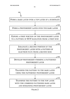
- The method involves forming a lithography stack with a silicon-based dielectric base layer and a photoresist layer, where the base layer acts as an electron booster to enhance exposure of the photoresist with energetic electrons, reducing the EUV radiation dose needed by 10-50% by promoting secondary exposure from below, thereby lowering the EUV radiation dose required for patterning.
Supply Chain Considerations for EUV Materials
The EUV lithography materials supply chain represents a critical component in the semiconductor manufacturing ecosystem, characterized by high complexity and strategic importance. Material procurement for EUV lithography involves specialized suppliers with advanced technical capabilities, creating potential bottlenecks in the global semiconductor supply network. Currently, the supply chain is concentrated among a limited number of providers, primarily located in Japan, the United States, and Western Europe, which introduces geopolitical vulnerabilities and regional dependencies.
Raw material sourcing presents significant challenges, particularly for rare elements required in photoresist formulations and specialized optical coatings. The limited availability of these materials, combined with growing demand from expanding EUV adoption, has created supply constraints that impact production schedules and pricing stability. Additionally, the high purity requirements for EUV materials necessitate specialized processing capabilities that further restrict supplier diversity.
Logistical considerations for EUV materials include specialized transportation requirements due to the sensitivity of photoresists and other chemical components to environmental conditions. Temperature-controlled shipping, contamination prevention protocols, and shelf-life limitations add complexity to the supply chain management process. These factors contribute to increased lead times and inventory management challenges for semiconductor manufacturers implementing EUV technology.
Supply chain resilience has emerged as a strategic priority following recent global disruptions. Semiconductor manufacturers are increasingly implementing multi-sourcing strategies for critical EUV materials where technically feasible. However, the specialized nature of many EUV materials limits complete diversification options. Industry consortia and strategic partnerships between material suppliers and semiconductor manufacturers are developing to ensure continuity of supply and collaborative problem-solving for material optimization.
Regulatory compliance adds another dimension of complexity to the EUV materials supply chain. Chemical substances used in photoresists and processing materials are subject to varying international regulations regarding transportation, handling, and environmental impact. Navigating these regulatory frameworks requires sophisticated compliance systems and increases administrative overhead throughout the supply chain.
Future supply chain evolution will likely involve greater vertical integration among key players, with major semiconductor manufacturers potentially acquiring or developing strategic partnerships with materials suppliers. Localization efforts are also underway in various regions to reduce dependency on cross-border material flows, though these initiatives face significant technical and economic challenges due to the specialized nature of EUV materials production.
Environmental Impact of EUV Material Processing
The environmental footprint of EUV lithography material processing represents a significant concern as semiconductor manufacturing advances. The chemicals used in EUV photoresist formulations often contain heavy metals and fluorinated compounds that pose substantial environmental risks if not properly managed. Current EUV material processing typically requires extensive use of solvents during development and etching stages, generating hazardous waste streams that require specialized treatment protocols.
Water consumption in EUV material processing deserves particular attention, as the ultra-pure water requirements for cleaning and processing steps can reach thousands of gallons per wafer. This intensive water usage occurs in an industry already under scrutiny for its resource demands, especially in water-stressed regions where many semiconductor facilities operate.
Energy consumption presents another environmental challenge, as EUV lithography systems require significant power for operation. The material modification processes themselves, including thermal annealing and plasma treatments used to enhance photoresist performance, contribute substantially to the carbon footprint of semiconductor manufacturing facilities.
Waste management systems for EUV material processing must address both solid and liquid waste streams containing photoresist residues, developer chemicals, and etching byproducts. The semiconductor industry has implemented advanced recycling and treatment technologies, but the unique chemistry of EUV materials often requires specialized handling that increases processing costs and complexity.
Regulatory frameworks governing EUV material processing vary globally, creating compliance challenges for multinational semiconductor manufacturers. The European Union's REACH regulations and similar initiatives in Asia and North America increasingly restrict the use of certain chemicals common in photoresist formulations, driving research toward more environmentally benign alternatives.
Industry initiatives have emerged to address these environmental concerns, including the development of "green photoresists" with reduced metal content and lower toxicity profiles. Material reclamation technologies that recover precious metals and reduce waste volumes are gaining traction, though their implementation at production scale remains limited.
Life cycle assessment studies of EUV lithography materials indicate that the environmental impact extends beyond manufacturing to include raw material extraction and end-of-life disposal. This holistic perspective has prompted semiconductor companies to pursue circular economy approaches, designing materials and processes with recyclability and reduced environmental persistence in mind.
Unlock deeper insights with Patsnap Eureka Quick Research — get a full tech report to explore trends and direct your research. Try now!
Generate Your Research Report Instantly with AI Agent
Supercharge your innovation with Patsnap Eureka AI Agent Platform!