

Exploring Semiconductor Materials for Neuromorphic Chips
OCT 9, 202510 MIN READ
Generate Your Research Report Instantly with AI Agent
PatSnap Eureka helps you evaluate technical feasibility & market potential.
Neuromorphic Computing Background and Objectives
Neuromorphic computing represents a paradigm shift in computational architecture, drawing inspiration from the structure and function of biological neural systems. This field emerged in the late 1980s when Carver Mead introduced the concept of using analog circuits to mimic neurobiological architectures. Since then, neuromorphic computing has evolved significantly, transitioning from purely academic research to practical applications in artificial intelligence, robotics, and edge computing.
The evolution of neuromorphic computing has been closely tied to advancements in semiconductor materials. Traditional CMOS technology, while foundational, presents limitations in emulating the brain's efficiency and parallel processing capabilities. This has driven research toward novel semiconductor materials that can better replicate neural functions such as spike-timing-dependent plasticity (STDP) and synaptic weight modulation.
Recent years have witnessed accelerated development in this field, propelled by the increasing demands of AI applications and the limitations of conventional von Neumann architectures in handling neural network computations. The neuromorphic chip market is projected to grow at a CAGR of approximately 20% through 2026, highlighting the increasing recognition of its potential to revolutionize computing paradigms.
The primary objective in exploring semiconductor materials for neuromorphic chips is to develop computing systems that can approach the human brain's remarkable energy efficiency—approximately 20 watts for cognitive functions—while delivering comparable computational capabilities. Current neuromorphic implementations still fall short of this benchmark by several orders of magnitude.
Another critical goal is to create systems capable of unsupervised learning and adaptation, similar to biological neural networks. This requires semiconductor materials that can exhibit plasticity and maintain stable states without continuous power consumption, properties not readily available in conventional silicon-based technologies.
The technical trajectory points toward increasing integration of diverse materials, including phase-change materials, memristive oxides, and two-dimensional semiconductors, each offering unique advantages for specific neural functions. Research is also focusing on 3D integration techniques to increase connection density and more accurately mimic the brain's complex interconnectivity.
As we advance, the convergence of material science, neuroscience, and computer engineering will likely accelerate innovations in this field, potentially leading to neuromorphic systems that can approach biological neural networks in terms of efficiency, adaptability, and cognitive capabilities.
Market Analysis for Brain-Inspired Computing Solutions
The brain-inspired computing market is experiencing unprecedented growth, driven by the increasing demand for efficient AI processing solutions that mimic human neural networks. Current market valuations place neuromorphic computing at approximately 3.2 billion USD in 2023, with projections indicating a compound annual growth rate of 23.7% through 2030. This remarkable expansion is fueled by applications across multiple sectors including autonomous vehicles, robotics, healthcare diagnostics, and edge computing devices.
Key market segments for neuromorphic semiconductor materials include memristive devices, phase-change materials, spintronic components, and organic electronics. Among these, memristive technologies currently dominate with nearly 42% market share due to their superior power efficiency and analog computing capabilities. Phase-change materials represent the fastest-growing segment at 29.3% CAGR, attributed to recent breakthroughs in reliability and manufacturing scalability.
Industry analysis reveals significant regional variations in market adoption. North America leads with 38% of global market share, bolstered by substantial research investments and strong presence of semiconductor giants. Asia-Pacific follows closely at 35%, with China and South Korea making aggressive investments in neuromorphic research facilities. Europe accounts for 22% of the market, distinguished by strong academic-industrial collaborations in materials science.
Consumer electronics represents the largest application vertical (31%), followed by automotive (24%), healthcare (18%), and defense (14%). The remaining 13% encompasses emerging applications in smart infrastructure and industrial automation. This distribution highlights the versatility of neuromorphic solutions across diverse industries.
Market barriers include high development costs, with average R&D investment for new neuromorphic materials exceeding 120 million USD before commercialization. Technical challenges in scaling production while maintaining performance consistency remain significant hurdles. Additionally, the fragmented ecosystem of hardware manufacturers, software developers, and end-users creates integration complexities that slow market penetration.
Customer demand analysis indicates shifting priorities, with energy efficiency now ranking as the primary purchase consideration (37%), followed by computational performance (29%), integration flexibility (22%), and cost (12%). This represents a notable shift from traditional semiconductor purchasing patterns where performance and cost traditionally dominated decision-making.
The competitive landscape features both established semiconductor manufacturers pivoting toward neuromorphic solutions and specialized startups focusing exclusively on brain-inspired architectures. Strategic partnerships between material scientists, chip designers, and AI software developers are increasingly common, creating integrated value chains that accelerate commercialization timelines.
Current Semiconductor Materials Landscape and Challenges
The semiconductor landscape for neuromorphic computing is currently dominated by traditional CMOS (Complementary Metal-Oxide-Semiconductor) technology, which has been adapted to implement neural network architectures. However, conventional CMOS faces fundamental limitations in power efficiency, speed, and density when mimicking the brain's parallel processing capabilities. Silicon-based neuromorphic chips from companies like Intel (Loihi) and IBM (TrueNorth) represent the most mature implementations but still consume orders of magnitude more power than biological systems.
Emerging non-volatile memory technologies are gaining significant traction as potential game-changers. Resistive Random Access Memory (RRAM), Phase Change Memory (PCM), and Magnetic RAM (MRAM) offer promising characteristics for implementing synaptic functions with their ability to store analog values and maintain states without power consumption. These materials enable direct implementation of spike-timing-dependent plasticity (STDP) and other learning mechanisms critical for neuromorphic systems.
Two-dimensional materials like graphene and transition metal dichalcogenides (TMDs) represent another frontier, offering exceptional electrical properties and scalability advantages. Their atomic thinness enables unprecedented device densities while maintaining good carrier mobility. However, manufacturing challenges and integration with existing fabrication processes remain significant hurdles.
Oxide-based materials, particularly metal oxides like HfO₂, TiO₂, and Ta₂O₅, have demonstrated remarkable memristive properties suitable for synaptic elements. These materials can be integrated into crossbar arrays to achieve high-density neural networks but face challenges in device variability and endurance.
Spintronic materials utilizing electron spin rather than charge are emerging as low-power alternatives. Magnetic tunnel junctions (MTJs) can implement neurons with inherent stochasticity that mimics biological behavior. While promising, spintronic devices currently suffer from reliability issues and complex fabrication requirements.
The primary technical challenges across these material platforms include achieving reliable analog states, reducing cycle-to-cycle and device-to-device variability, improving endurance for learning applications requiring millions of write cycles, and developing scalable manufacturing processes compatible with existing semiconductor infrastructure.
Energy efficiency remains a critical bottleneck, with even the most advanced neuromorphic chips consuming significantly more power per operation than biological neurons. Material interfaces and integration challenges further complicate the development of practical neuromorphic systems, as hybrid approaches combining multiple material systems often introduce additional complexity and reliability concerns.
Geographically, research leadership is distributed across North America (IBM, Intel, academic institutions), Europe (CEA-Leti, IMEC), and East Asia (Samsung, TSMC, Chinese Academy of Sciences), with each region focusing on different material approaches and integration strategies.
Current Semiconductor Material Solutions for Neural Networks
01 Phase-change materials for neuromorphic computing
Phase-change materials (PCMs) are semiconductor materials that can rapidly switch between amorphous and crystalline states, making them ideal for neuromorphic computing applications. These materials exhibit properties that mimic synaptic behavior, allowing for the implementation of artificial neural networks in hardware. PCMs can store multiple states, enabling analog-like computation necessary for brain-inspired computing architectures. Their non-volatile nature and scalability make them promising candidates for energy-efficient neuromorphic chips.- Phase-change materials for neuromorphic computing: Phase-change materials (PCMs) are semiconductor materials that can switch between amorphous and crystalline states, exhibiting different electrical resistances. These materials are particularly suitable for neuromorphic chips as they can mimic synaptic behavior through their ability to store multiple resistance states. PCMs enable efficient implementation of synaptic plasticity mechanisms required for learning and memory functions in neuromorphic systems.
- Resistive random-access memory (RRAM) materials: RRAM materials are semiconductor-based structures that can change resistance states when subjected to electrical stimuli. These materials are ideal for neuromorphic computing as they can emulate synaptic functions through their variable resistance states. RRAM devices typically use metal oxides or chalcogenides as the active switching layer, offering advantages such as low power consumption, high density, and compatibility with CMOS fabrication processes.
- Two-dimensional (2D) semiconductor materials: Two-dimensional semiconductor materials, such as transition metal dichalcogenides (TMDs), graphene, and black phosphorus, offer unique properties for neuromorphic computing applications. Their atomically thin nature allows for excellent electrostatic control, reduced short-channel effects, and tunable bandgaps. These materials can be used to create ultra-thin, flexible neuromorphic devices with high performance and energy efficiency, enabling novel architectures for brain-inspired computing.
- Ferroelectric materials for neuromorphic devices: Ferroelectric semiconductor materials exhibit spontaneous electric polarization that can be reversed by applying an external electric field. This property makes them excellent candidates for neuromorphic computing as they can implement non-volatile memory functions with low power consumption. Ferroelectric field-effect transistors (FeFETs) and ferroelectric tunnel junctions (FTJs) based on materials like hafnium oxide or barium titanate can efficiently mimic synaptic behavior for neuromorphic applications.
- Memristive semiconductor materials: Memristive semiconductor materials exhibit the ability to remember their history of applied current or voltage, making them ideal for implementing artificial synapses and neurons. These materials, including metal oxides, chalcogenides, and organic semiconductors, can maintain their resistance state without power, enabling energy-efficient neuromorphic computing. Their analog switching behavior allows for the implementation of spike-timing-dependent plasticity and other learning mechanisms essential for brain-inspired computing systems.
02 Resistive switching materials for synaptic devices
Resistive switching materials are semiconductor compounds that can change their resistance states in response to electrical stimuli, similar to biological synapses. These materials include metal oxides and chalcogenides that can be integrated into resistive random-access memory (RRAM) structures for neuromorphic applications. The ability to gradually change resistance values enables these materials to mimic synaptic plasticity, a key requirement for learning and memory in neural networks. Their low power consumption and high integration density make them suitable for large-scale neuromorphic systems.Expand Specific Solutions03 Two-dimensional materials for neuromorphic devices
Two-dimensional (2D) semiconductor materials such as graphene, transition metal dichalcogenides (TMDs), and hexagonal boron nitride (h-BN) offer unique properties for neuromorphic computing. Their atomically thin nature allows for excellent electrostatic control and reduced power consumption. These materials exhibit tunable electronic properties and can be stacked in various configurations to create heterostructures with specific functionalities. The high carrier mobility and mechanical flexibility of 2D materials make them promising candidates for next-generation neuromorphic chips that require both high performance and adaptability.Expand Specific Solutions04 Silicon-based neuromorphic architectures
Silicon remains a fundamental semiconductor material for neuromorphic computing due to its compatibility with conventional CMOS technology. Advanced silicon-based neuromorphic architectures incorporate specialized circuit designs that mimic neural functions while leveraging established manufacturing processes. These include silicon neurons, dendrites, and synaptic elements that can be integrated at high density. Silicon photonics is also emerging as a promising approach, using light for neural signal processing. The maturity of silicon technology enables rapid scaling and integration of neuromorphic systems with conventional computing platforms.Expand Specific Solutions05 Emerging materials for quantum neuromorphic computing
Novel semiconductor materials are being explored for quantum neuromorphic computing, which combines principles of quantum mechanics with neural network architectures. These include superconducting materials, topological insulators, and quantum dots that can maintain quantum coherence while performing neural computations. Such materials enable the implementation of quantum neural networks that can potentially solve complex problems beyond the capabilities of classical neuromorphic systems. The integration of quantum effects in neuromorphic computing could lead to exponential increases in computational power while maintaining energy efficiency.Expand Specific Solutions
Leading Companies and Research Institutions in Neuromorphic Computing
The neuromorphic chip market is in its early growth phase, characterized by significant R&D investments but limited commercial deployment. Market size is projected to expand rapidly as brain-inspired computing gains traction in AI applications, with estimates suggesting a CAGR of 20-30% over the next five years. Technologically, the field shows varying maturity levels across players: IBM and Samsung lead with established research programs and functional prototypes; Syntiant has commercialized edge AI solutions; while academic institutions (KAIST, Fudan University, MIT) contribute fundamental research. Semiconductor manufacturers like SK Hynix, Micron, and Renesas are exploring novel materials integration. The competitive landscape features collaboration between industry leaders and research institutions, with specialized startups emerging to address niche applications in this promising but still-developing technology domain.
International Business Machines Corp.
Technical Solution: IBM has pioneered neuromorphic computing with their TrueNorth and subsequent chip architectures. Their approach focuses on phase-change memory (PCM) materials for synaptic functions in neuromorphic systems. IBM's research utilizes chalcogenide-based PCM, particularly Ge2Sb2Te5 (GST), which can maintain multiple resistance states to mimic biological synapses. Their technology demonstrates spike-timing-dependent plasticity (STDP) learning rules through precise control of crystallization states in these materials. IBM has achieved energy efficiency of approximately 20 pJ per synaptic event, significantly lower than conventional CMOS implementations. Their neuromorphic chips integrate millions of artificial neurons and synapses on a single chip, with recent iterations achieving densities of over 1 million synapses per square millimeter. The company has also explored integrating these semiconductor materials with traditional CMOS technology to create hybrid neuromorphic systems that leverage the strengths of both approaches.
Strengths: IBM's extensive experience in semiconductor research provides them with advanced fabrication capabilities and deep material science expertise. Their neuromorphic designs show excellent power efficiency and high integration density. Weaknesses: The phase-change materials used still face challenges with long-term stability and endurance limitations, potentially affecting the reliability of neuromorphic systems in extended operation.
Samsung Electronics Co., Ltd.
Technical Solution: Samsung has developed neuromorphic chip technology based on resistive random-access memory (RRAM) and magnetoresistive random-access memory (MRAM) materials. Their approach utilizes hafnium oxide-based RRAM structures that demonstrate analog switching behavior suitable for synaptic weight implementation. Samsung's neuromorphic semiconductor materials incorporate oxygen-deficient metal oxides that enable precise control of conductance states through ion migration mechanisms. Their research has demonstrated successful implementation of these materials in crossbar array architectures, achieving synapse densities exceeding 10^9 per cm². Samsung has also explored three-dimensional integration of these memory elements, stacking multiple layers of neuromorphic circuits to increase computational density while maintaining energy efficiency. Recent developments include the incorporation of 2D materials like MoS2 as channel materials in their neuromorphic transistor designs, which has shown improved switching characteristics and lower operating voltages compared to conventional oxide-based devices. Samsung's neuromorphic chips have demonstrated on-chip learning capabilities with energy consumption as low as 1-10 femtojoules per synaptic operation.
Strengths: Samsung possesses extensive manufacturing infrastructure and expertise in memory technologies, allowing rapid scaling and commercialization of neuromorphic designs. Their materials show excellent compatibility with existing semiconductor fabrication processes. Weaknesses: Their RRAM-based approach still faces challenges with device-to-device variability and cycle-to-cycle variations that can impact the reliability and precision of neural network implementations.
Key Innovations in Memristive and Phase-Change Materials
Patent
Innovation
- Development of phase-change materials with tunable resistance states for neuromorphic computing, enabling efficient synaptic weight storage and mimicking biological neural networks.
- Integration of memristive devices based on oxide semiconductors that demonstrate spike-timing-dependent plasticity (STDP), allowing for unsupervised learning capabilities in hardware.
- Novel semiconductor heterostructures that facilitate multi-level resistance states, enabling higher density information storage and more complex neural network implementations.
Neuromorphic semiconductor device and operating method thereof
PatentPendingUS20250157556A1
Innovation
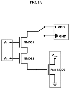
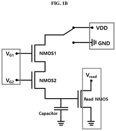
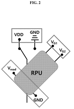
- A neuromorphic semiconductor device utilizing a resistive processing unit (RPU) with N-type metal oxide semiconductor (NMOS) elements, enabling symmetrical charging/discharging and memory updates, and reducing off-current by connecting NMOSs in series.
Energy Efficiency Considerations for Brain-Inspired Chips
Energy efficiency represents a critical factor in the development and deployment of neuromorphic computing systems. Traditional von Neumann architectures face significant energy constraints when implementing neural network operations, with power consumption becoming prohibitively high as complexity increases. Neuromorphic chips, designed to mimic the brain's neural structure, offer promising alternatives by potentially reducing energy requirements by several orders of magnitude.
The human brain operates on approximately 20 watts of power while performing complex cognitive tasks that would require megawatts in conventional computing systems. This remarkable efficiency stems from the brain's architecture, which processes information through massively parallel, event-driven operations rather than sequential, clock-driven computations. Semiconductor materials play a pivotal role in achieving similar efficiencies in neuromorphic hardware.
Novel semiconductor materials such as hafnium oxide, tantalum oxide, and various chalcogenides demonstrate properties conducive to low-power neuromorphic operations. These materials facilitate resistive switching mechanisms that can maintain states with minimal energy input, allowing for persistent memory without continuous power consumption. Phase-change materials (PCMs) like germanium-antimony-tellurium (GST) compounds offer non-volatile memory capabilities with switching energies in the picojoule range, significantly lower than conventional CMOS memory technologies.
The integration of these advanced materials with traditional CMOS processes presents both opportunities and challenges. Hybrid approaches combining the computational efficiency of CMOS with the memory capabilities of emerging materials show promise for optimizing energy consumption. Three-dimensional integration techniques further enhance energy efficiency by reducing interconnect distances and associated parasitic capacitances.
Power management strategies specific to neuromorphic systems include spike-based communication protocols that transmit information only when necessary, dramatically reducing dynamic power consumption. Adaptive power gating techniques can selectively deactivate inactive neural circuits, while maintaining essential network functionality. These approaches align with the brain's strategy of conserving energy through selective activation.
Benchmarking studies indicate that current neuromorphic implementations achieve energy efficiencies ranging from 10^-12 to 10^-15 joules per synaptic operation, compared to 10^-10 joules in conventional digital systems. However, significant challenges remain in scaling these efficiencies while maintaining computational accuracy and reliability. Material stability, interface degradation, and variability issues must be addressed to ensure consistent performance across large-scale neuromorphic systems.
Future directions for energy optimization include exploration of two-dimensional materials like graphene and transition metal dichalcogenides, which offer atomic-scale thickness and unique electronic properties that could further reduce switching energies. Quantum-inspired materials that leverage coherent electron states may eventually provide pathways to ultra-low-energy computing paradigms beyond current thermodynamic limits.
Integration Pathways with Conventional Computing Architectures
The integration of neuromorphic computing systems with conventional computing architectures represents a critical pathway for the broader adoption of brain-inspired computing technologies. Current semiconductor materials for neuromorphic chips must be compatible with existing CMOS fabrication processes to ensure cost-effective manufacturing and seamless integration into established computing ecosystems.
One promising integration approach involves hybrid architectures that combine neuromorphic processing units with traditional von Neumann processors. This heterogeneous integration allows systems to leverage the strengths of both paradigms—conventional architectures excel at precise, sequential operations while neuromorphic components handle pattern recognition and parallel processing tasks. Silicon interposers and through-silicon vias (TSVs) provide physical integration pathways, enabling high-bandwidth, low-latency communication between these disparate computing elements.
Memory-centric integration represents another significant pathway, particularly as neuromorphic systems often require substantial memory resources for synaptic weight storage. Emerging non-volatile memory technologies such as RRAM, PCM, and MRAM can serve dual purposes as both memory elements and neuromorphic computing components, creating natural integration points with conventional memory hierarchies. This approach minimizes data movement between processing and memory units, addressing the von Neumann bottleneck that plagues traditional computing systems.
From a software perspective, neuromorphic-conventional integration necessitates specialized compilers and runtime systems that can efficiently map applications across heterogeneous computing resources. Neuromorphic development frameworks like Intel's Loihi SDK and IBM's TrueNorth Neurosynaptic System provide programming abstractions that bridge the conceptual gap between conventional and neuromorphic programming models.
Power management integration presents unique challenges, as neuromorphic systems typically operate at significantly lower power levels than conventional processors. Advanced power delivery networks must accommodate these disparate requirements, potentially incorporating separate power domains with specialized voltage regulators for neuromorphic components. Silicon-based power management ICs (PMICs) fabricated using conventional CMOS processes can provide this functionality while maintaining compatibility with both computing paradigms.
Looking forward, chiplet-based integration approaches show particular promise, allowing neuromorphic elements to be manufactured as separate dies and then integrated with conventional computing components using advanced packaging technologies. This modular approach enables independent optimization of semiconductor materials for each computing paradigm while maintaining system-level integration through standardized interfaces like UCIe (Universal Chiplet Interconnect Express).
Unlock deeper insights with PatSnap Eureka Quick Research — get a full tech report to explore trends and direct your research. Try now!
Generate Your Research Report Instantly with AI Agent
Supercharge your innovation with PatSnap Eureka AI Agent Platform!